1
M
e
m
o
r
y
All data sheets are subject to change without notice
(858) 503-3300 - Fax: (858) 503-3301 - www.maxwell.com
1.25Gb SDRAM
8-Meg X 40-Bit X 4-Banks
©2005 Maxwell Technologies
All rights reserved.
97SD3240
02.04.05 Rev 3
F
EATURES
:
∑ 1.25 Gigabit ( 8-Meg X 40-Bit X 4-Banks)
∑ RAD-PAKÆ radiation-hardened against natural space
radiation
∑ Total Dose Hardness:
>100 krad (Si), depending upon space mission
∑ Excellent Single Event Effects:
SEL
TH
> 85 MeV/mg/cm2 @ 25∞C
∑ JEDEC Standard 3.3V Power Supply
∑ Clock Frequency: 100 MHz Operation
∑ Operating tremperature: -55 to +125 ∞C
∑ Auto Refresh
∑ Single pulsed RAS
∑ 2 Burst Sequence variations
Sequential (BL =1/2/4/8)
Interleave (BL = 1/2/4/8)
∑ Programmable CAS latency: 2/3
∑ Power Down and Clock Suspend Modes
∑ LVTTL Compatible Inputs and Outputs
∑ Package: 132 Lead Quad Stack Pack Flat Package
D
ESCRIPTION
:
Maxwell Technologies' Synchronous Dynamic Random
Access Memory (SDRAM) is ideally suited for space
applications requiring high performance computing and
high density memory storage. As microprocessors
increase in speed and demand for higher density mem-
ory escalates, SDRAM has proven to be the ultimate
solution by providing bit-counts up to 1.25 Gigabits and
speeds up to 100 Megahertz. SDRAMs represent a sig-
nificant advantage in memory technology over traditional
DRAMs including the ability to burst data synchronously
at high rates with automatic column-address generation,
the ability to interleave between banks masking pre-
charge time
Maxwell Technologies' patented R
AD
-P
AK
Æ
packaging
technology incorporates radiation shielding in the micro-
circuit package. It eliminates the need for box shielding
for a lifetime in orbit or space mission. In a typical GEO
orbit, R
AD
-P
AK
Æ
provides greater than 100 krads(Si)
radiation dose tolerance. This product is available with
screening up to Maxwell Technologies self-defined Class
K.
Logic Diagram
(One Amplifier)

97SD3240
M
e
m
o
r
y
2
All data sheets are subject to change without notice
©2005 Maxwell Technologies
All rights reserved.
1.25Gb (8-Meg X 40-Bit X 4-Banks) SDRAM
02.04.05 Rev 3
Pinout Description
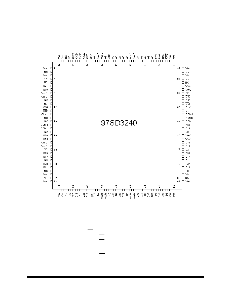
The 97SD3240 Consists of 5, 8-Meg X 8-Bit X 4-Banks, die.
CKE 1-5, CS 1-5 and DQM 1-5 correspond to one of the die:
CKE1, CS1 and DQM1 control D0 - D7
CKE2, CS2 and DQM2 control D8 - D15
CKE3, CS3 and DQM3 control D16 - D23
CKE4, CS4 and DQM4 control D24 - D31
CKE5, CS5 and DQM5 control D32 - D39
The 132 Pin 3-layer stack package contains 2die in layer one
and two and one die in layer three. CLK1 clocks die 1, 3 and 5,
while CLK2 clocks die 2 and 4.

97SD3240
M
e
m
o
r
y
3
All data sheets are subject to change without notice
©2005 Maxwell Technologies
All rights reserved.
1.25Gb (8-Meg X 40-Bit X 4-Banks) SDRAM
02.04.05 Rev 3
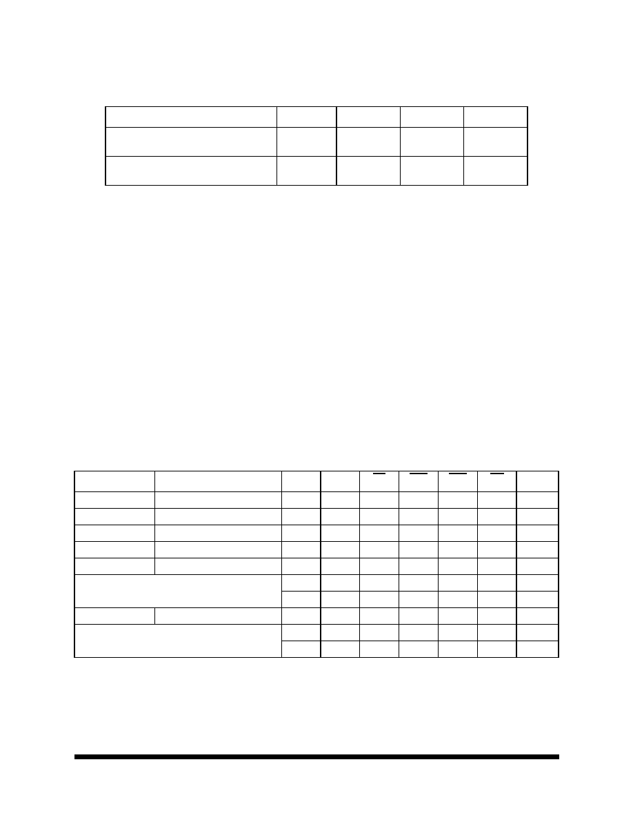
`
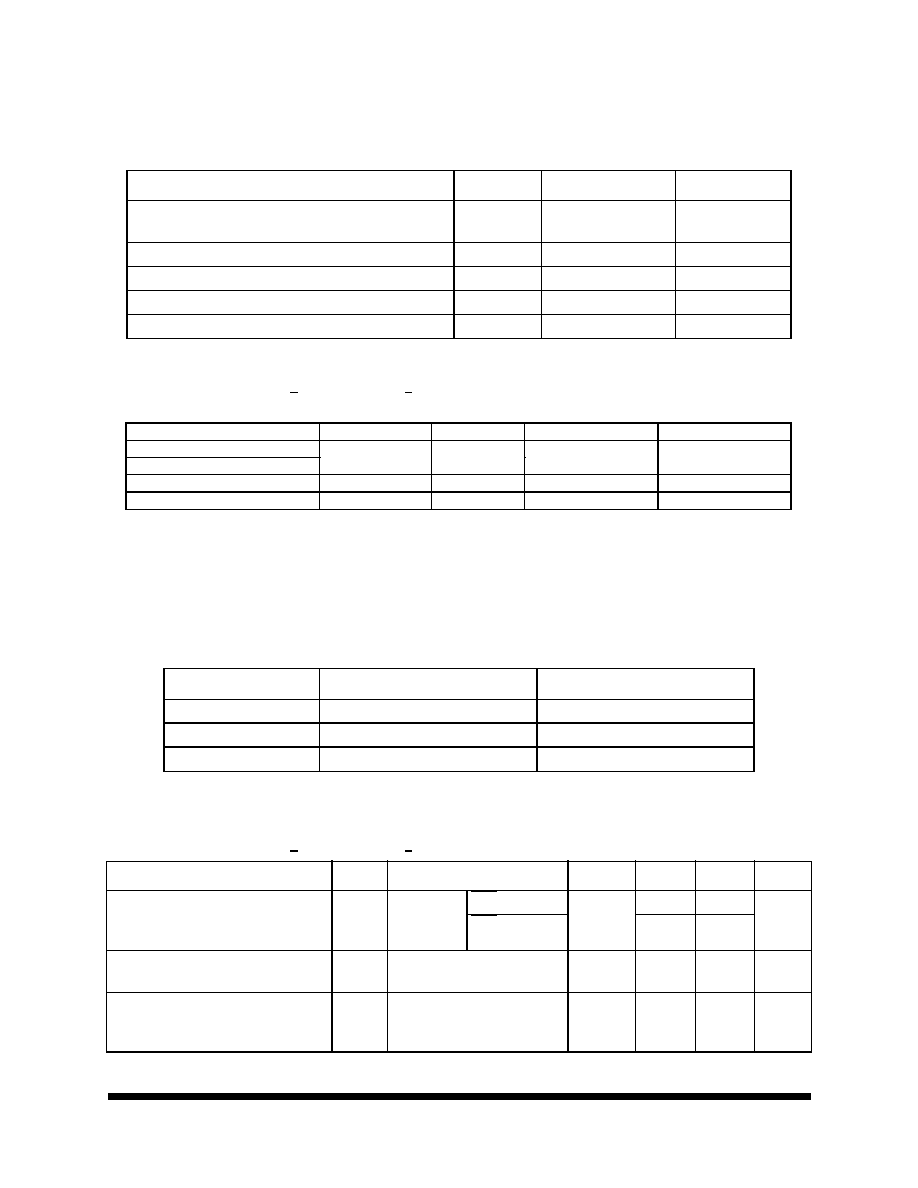
T
ABLE
1. A
BSOLUTE
M
AXIMUM
R
ATINGS
P
ARAMETER
S
YMBOL
M
AX
U
NIT
Voltage on any pin relative to V
SS
V
IN
V
OUT
-0.5 to VCC + 0.5
(< 4.6(max))
V
Supply voltage relative to V
SS
V
CC
-0.5 to +4.6
V
Short circuit output current
I
OUT
50
mA
Operating Temperature
T
OPR
-55 to +125
∞C
Storage Temperature
T
STG
-65 to +150
∞C
T
ABLE
2. R
ECOMMENDED
O
PERATING
C
ONDITIONS
(V
CC
= 3.3V + 0.3V, V
CC
Q = 3.3V + 0.3V, T
A
= -55
TO
125∞C,
UNLESS
OTHERWISE
SPECIFIED
)
T
ABLE
3. D
ELTA
L
IMITS
P
ARAMETER
D
ESCRIPTION
V
ARIATION1
1. ±10% of value specified in Table 4
I
CC1
Operating Current
±10%
I
CC2P
I
CC2PS
I
CC2N
I
CC2NS
Power Down Standby Current
±10%
I
CC3P
I
CC3PS
I
CC3N
I
CC3NS
Active Standby Current
±10%
T
ABLE
4. DC E
LECTRICAL
C
HARACTERISTICS
(V
CC
= 3.3V + 0.3V, V
CC
Q = 3.3V + 0.3V, T
A
= -55
TO
125∞C,
UNLESS
OTHERWISE
SPECIFIED
)
P
ARAMETER
S
YMBOL
T
EST
C
ONDITIONS
S
UBGROUPS
M
IN
M
AX
U
NITS
Operating Current
1,2,3
I
CC1
Burst length
= 1
t
RC
= min
CAS Latency = 2
1, 2, 3
575
mA
CAS Latency = 3
575
Standby Current in Power Down
4
I
CC2P
CKE = V
IL
t
CK
= 12 ns
1, 2, 3
15
mA
Standby Current in Power Down
( input signal stable)
5
I
CC2PS
CKE = V
IL
t
CK
= 0
1, 2, 3
10
mA
P
ARAMETER
S
YMBOL
M
IN
M
AX
U
NIT
Supply Voltage
V
CC
, V
CCQ
1,2
3.0
3.6
V
V
SS
, V
SSQ
3
0
0
V
Input High Voltage
V
IH
1,4
2.0
V
CC
+ 0.3
V
Input Low Voltage
V
IL1,5
-0.3
0.8
V
1. All voltage referred to VSS
2. The supply voltage with all
V
CC
and V
CCQ
pins must be on the same level
3. The supply voltage with all V
SS
and V
SSQ
pins must be on the same level
4.
V
IH
(max) =
V
CC
+2.0V for pulse width
<3ns at V
CC
5.
V
IL
(min) =
V
SS
-2.0V for pulse width
<3ns at V
SS

97SD3240
M
e
m
o
r
y
4
All data sheets are subject to change without notice
©2005 Maxwell Technologies
All rights reserved.
1.25Gb (8-Meg X 40-Bit X 4-Banks) SDRAM
02.04.05 Rev 3
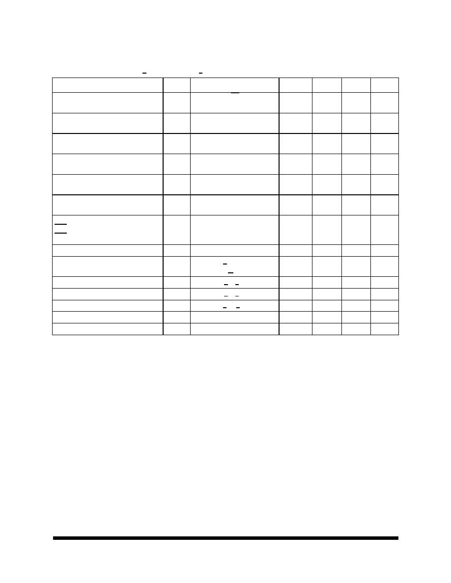
Standby Current in non power down
6
I
CC2N
CKE, CS = V
IH
t
CK
= 12 ns
1, 2, 3
100
mA
Standby Current in non power down
7
( Input signal stable)
I
CC2NS
CKE = V
IH
t
CK
= 0
1, 2, 3
45
mA
Active standby current in
1,2,4
power down
I
CC3P
CKE = V
IL
t
CK
= 12 ns
1, 2, 3
20
mA
Active standby current in power down
(input signal stable)
2,5
I
CC3PS
CKE = V
IL
t
CK
= 0
1, 2, 3
15
mA
Active standby power in non power
down
1,2,6
I
CC3N
CKE, CS1-6 = V
IH
t
CK
= 12 ns
1, 2, 3
150
mA
Active standby current in non power
down ( input signal stable)
2,7
I
CC3NS
CKE = V
IH
t
CK
= 0
1, 2, 3
75
mA
Burst Operating Current
1,2,8
CAS Latency = 2
CAS Latency = 3
I
CC4
t
CK
= min
BL = 4
1, 2, 3
550
725
mA
Refresh Current
3
I
CC5
t
RC
= min
1, 2, 3
1100
mA
Self Refresh current
9
I
CC6
V
IH
>V
CC
- 0.2V
V
IL
< 0.2 V
1, 2, 3
15
mA
Input Leakage Current - CLK
I
LI
0<V
LI
<V
CC
1, 2, 3
-3
3
uA
Input Leakage Current - All Other
I
LI
0<V
LI
<V
CC
1, 2, 3
-5
5
uA
Output Leakage Current
I
LO
0<V
LO
<V
CC
1, 2, 3
-1.5
1.5
uA
Output high voltage
V
OH
I
OH
= -4mA
1, 2, 3
2.4
V
Output low voltage
V
OL
I
OL
= 4 mA
1, 2, 3
0.4
V
1. I
CC1
depends on output load conditions when the device is selected. I
CC1
(max) is specified with the output open.
2. One Bank Operation
3. Input signals are changed once per clock.
4. After power down mode, CLK operating current.
5. After power down mode, no CLK operating current.
6. Input signals are changed once per two clocks.
7. Input signals for V
IH
or V
IL
are fixed.
8. Input signals are changed once per four clocks.
9. After self refresh mode set, self refresh current. Use Self Refresh for temperatures less than 70 ∞C O
NLY
.
T
ABLE
4. DC E
LECTRICAL
C
HARACTERISTICS
(V
CC
= 3.3V + 0.3V, V
CC
Q = 3.3V + 0.3V, T
A
= -55
TO
125∞C,
UNLESS
OTHERWISE
SPECIFIED
)
P
ARAMETER
S
YMBOL
T
EST
C
ONDITIONS
S
UBGROUPS
M
IN
M
AX
U
NITS

97SD3240
M
e
m
o
r
y
5
All data sheets are subject to change without notice
©2005 Maxwell Technologies
All rights reserved.
1.25Gb (8-Meg X 40-Bit X 4-Banks) SDRAM
02.04.05 Rev 3
T
ABLE
5. AC Electrical Characteristics
(V
CC
=3.3V + 0.3V, V
CC
Q = 3.3V + 0.3V, T
A
= -55
TO
125∞C,
UNLESS
OTHERWISE
SPECIFIED
)
P
ARAMETER
S
YMBOL
S
UBGROUPS
M
IN
T
YPICAL
M
AX
U
NIT
System clock cycle time
1
(CAS latency = 2)
(CAS latency = 3)
t
CK
9, 10, 11
10
7.5
ns
CLK high pulse width
1,7
t
CKH
9, 10, 11
2.5
ns
CLK low pulse width
1,7,
t
CKL
9, 10, 11
2.5
ns
Access time from CLK
1,2
(CAS latency = 2)
(CAS latency = 3)
t
AC
9, 10, 11
6
6
ns
Data-out hold time
1,2,3
t
OH
9, 10, 11
2.7
ns
CLK to Data-out low impedance
1,2,3,7
t
LZ
9, 10, 11
2
ns
CLK to Data-out high impedance
1,47,
(CAS latency = 2, 3)
t
HZ
9, 10, 11
5.4
ns
Input setup time
1,5,6
t
AS
, t
CS,
t
DS
, t
CES
9, 10, 11
1.5
ns
CKE setup time for power down exit
1
t
CESP
9, 10, 11
1.5
ns
Input hold time
1,6
t
AH
, t
CH
, t
DH
t
CEH
9, 10, 11
1.5
ns
Ref/Active to Ref/Active command period
1
t
RC
9, 10, 11
70
ns
Active to Precharge command period
1
t
RAS
9, 10, 11
50
120000
ns
Active command to column command
1
(same bank)
t
RCD
9, 10, 11
20
ns
Precharge to Active command period
1
t
RP
9, 10, 11
20
ns
Write recovery or data-in to precharge lead time
1
t
DPL
9, 10, 11
20
ns
Active( a) to Active (b) command period
1
t
RRD
9, 10, 11
20
ns
Transition time(rise and fall)
7
t
T
9, 10, 11
1
5
ns
Refresh Period
t
REF
9, 10, 11
16
6.4
ms
@ 105 ∞C
32
16
8
@ 85 ∞C
64
@ 70 ∞C
128
1. AC measurement assumes t
T
=1ns. Reference level for timing of input signals is 1.5V.
2. Access time is measured at 1.5V.
3. t
LZ
(min) definesthe time at which the outputs achieve the low impedance state.
4. t
HZ
(min) defines the time at which the outputs achieve the high impedance state.
5. tCES defines CKE setup time to CLK rising edge except for the power down exit command.
6. t
AS
/t
AH
: Address, t
CS
/t
CH
: /RAS, /CAS, /WE, DQM
7. Guarenteed by design (Not tested).
8. Guarenteed by Device Charactreization Testing. (Not 100% Tested)

97SD3240
M
e
m
o
r
y
6
All data sheets are subject to change without notice
©2005 Maxwell Technologies
All rights reserved.
1.25Gb (8-Meg X 40-Bit X 4-Banks) SDRAM
02.04.05 Rev 3
T
ABLE
6. C
APACITANCE1
P
ARAMETER
S
YMBOL
M
AX
U
NIT
Input Capacitance (CLK)
C
I1
17.5
pF
Input Capacitance (all other inputs)
C
I2
19
pF
Output Capacitance (DQ)
C
O
4
pF
1. Guarenteed by design.

97SD3240
M
e
m
o
r
y
7
All data sheets are subject to change without notice
©2005 Maxwell Technologies
All rights reserved.
1.25Gb (8-Meg X 40-Bit X 4-Banks) SDRAM
02.04.05 Rev 3
Pin Functions:
CLK (
INPUT
PIN
): CLK is the master clock input to this pin. The other input signals are referred at CLK rising
edge.
CS 1-5 (
INPUT
PINS
): When CS 1-5 are low, the command input cycle becomes valid. When CS 1-5 are High,
all inputs are ignored. However, internal operations (bank active, burst operations, etc.) are held.
RAS, CAS
AND
WE (
INPUT
PINS
): Although these pin names are the same as those of conventional DRAMs,
they function in a different way. These pins define operation commands (read, write, etc.) depending on the
combination of their voltage levels.
A0
TO
A12 (
INPUT
PINS
): Row address (AX0 to AX12) is determined by A0 to A12 level at the bank active
command cycle CLK rising edge. Column address (AY0 to AY9) is determined by A0 to A9 level at the read
or write command cycle CLK rising edge. And this column address becomes burst access start address.
A10 defines the precharge mode. When A10 = High at the precharge command cycle, all banks are pre-
charged. But when A10 = Low at the precharge command cycle, only the bank that is selected by BA0/BA1
(BS) is pre charged.
BA0/BA1 (
INPUT
PINS
): BA0/BA1 are bank select signals (BS). The memory array of the 97SD3240 is divided
into bank 0, bank 1, bank 2 and bank 3. The 97SD3240 contains 8192-row X 1024-column X 40-bit. If BA0
and BA1 is Low, bank 0 is selected. If BA0 is Low and BA1 is High, bank 1 is selected. If BA0 is High and
BA1 is Low, bank 2 is selected. If BAO is High and BA1 is High, bank 3 is selected.
CKE 1-5 (
INPUT
PIN
): This pin determines whether or not the next CLK is valid. If CKE 1-5 is High, the next
CLK rising edge is valid. If CKE 1-5 is Low, the next CLK rising edge is invalid. This pin is used for power-
down mode, clock suspend mode and self refresh mode
1
.
DQM 1-5 (
INPUT
PINS
): DQM 1-5 control input/output buffers
Read operation: If DQM 1-5 are High, the output buffer becomes High-Z. If the DQM 1-5 are Low, the output
buffer becomes Low-Z. ( The latency of DQM 1-5 during reading is 2 clock cycles.)
Write operation: If DQM 1-5 are High, the previous data is held ( the new data is not written). If the DQM 1-5
areLow, the data is written. ( The latency of DQM 1-5 during writing is 0 clock cycles.)
DQ0
TO
DQ39 (DQ
PINS
): Data is input to and output from these pins ( DQ0 to DQ39).
V
CC
AND
V
CC
Q (
POWER
SUPPLY
PINS
): 3.3V is applied. ( V
CC
is for the internal circuit and V
CC
Q is for the output
buffer.)
V
SS
AND
V
SS
Q (
POWER
SUPPLY
PINS
): Ground is connected. (V
SS
is for the internal circuit and V
SS
Q is for the
output buffer.)
1. Self refresh mode should only be used at temperatures below 70∞C.

97SD3240
M
e
m
o
r
y
8
All data sheets are subject to change without notice
©2005 Maxwell Technologies
All rights reserved.
1.25Gb (8-Meg X 40-Bit X 4-Banks) SDRAM
02.04.05 Rev 3
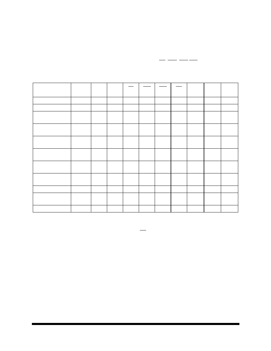
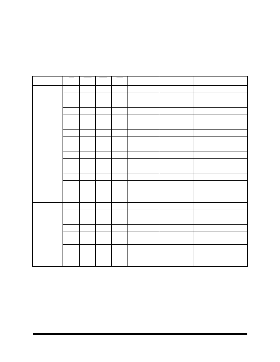
Command Operation
Command Truth Table
The SDRAM recognizes the following commands specified by the CS, RAS, CAS, WE and address pins:
Note: H: V
IH
L: V
IL
x V
IH
or V
IL
V: Valid address input
Ignore command (DESL): When this command is set (CS = High), the SDRAM ignores command input at
the clock. However, the internal status is held.
No Operation (NOP): This command is not an execution command. However, the internal operations
continue.
Column address strobe and read command (READ): This command starts a read operation. In addition,
the start address of a burst read is determined by the column address (AY0 to AY9) and the bank select
address (BS). After the read operation, the output buffer becomes High-Z.
Read with auto-precharge (READ A): This command automatically performs a precharge operation after a
burst read with a burst length of 1, 2, 4, or 8.
C
OMMAND
S
YMBOL
N
-1
N
CS
RAS
CAS
WE
BA0/
BA1
A10
A0
TO
A12
Ignore command
DESL
H
x
H
x
x
x
x
x
x
No Operation
NOP
H
x
L
H
H
H
x
x
x
Column Address and
Read command
READ
H
x
L
H
L
H
V
L
V
Read with auto-pre-
charge
READ A
H
x
L
H
L
H
V
H
V
Column Address and
write command
WRIT
H
x
L
H
L
L
V
L
V
Write with auto-pre-
charge
WRIT A
H
x
L
H
L
L
V
H
V
Row address strobe
and bank active
ACTV
H
x
L
L
H
H
V
V
V
Precharge select
bank
PRE
H
x
L
L
H
L
V
L
x
Precharge all banks
PALL
H
x
L
L
H
L
x
H
x
Refresh
REF/
SELF
H
L
L
L
L
H
x
x
x
Mode register set
MRS
H
x
L
L
L
L
V
V
V

97SD3240
M
e
m
o
r
y
9
All data sheets are subject to change without notice
©2005 Maxwell Technologies
All rights reserved.
1.25Gb (8-Meg X 40-Bit X 4-Banks) SDRAM
02.04.05 Rev 3
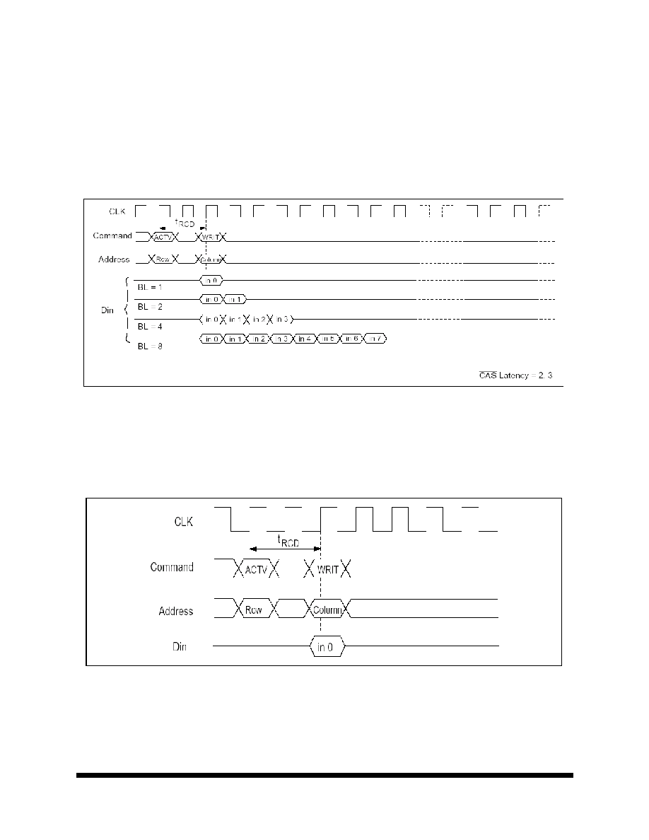
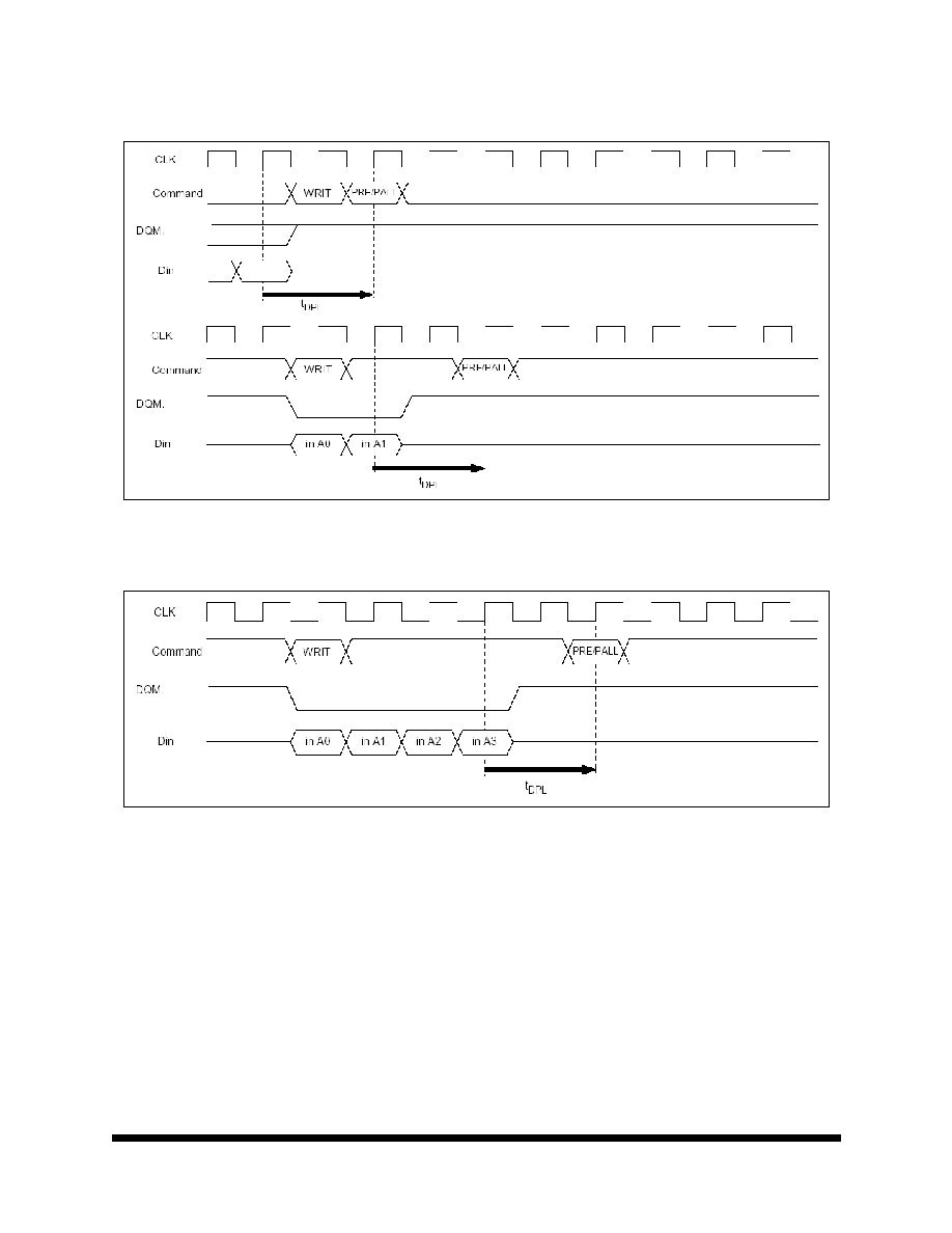
Column address strobe and write command (WRIT): This command starts a write operation. When the
burst write mode is selected, the column address (AY0 to AY9) and the bank select address (BA0/BA1)
become the burst write start address. When the single write mode is selected, data is only written to the
location specified by the column address (AY0 to AY9) and bank select address(BA0/BA1).
Write with auto-precharge (WRIT A): This command automatically performs a precharge operation after a
burst write with a length of 1, 2, 4, or 8, or after a single write operation.
Row address strobe and bank activate ( ACTV): This command activates the bank that is selected by
BA0/BA1 (BS) and determines the row address (AX0 to AX12). When BA0 and BA1 are Low, bank 0 is
activated. When BA0 is Low, and BA1 is High, bank 1 is activated. When BA0 is High and BA1 is Low, bank
2 is activated. When BA0 and BA1 are High, bank 3 is activated.
Precharge select bank (PRE): This command starts precharge operation for the bank selected by BA0/
BA1. If BA0 and BA1 are Low, bank 0 is selected. If BA0 is Low and BA1 is High, bank 1 is selected. If BA0
is High and BA1 is Low, bank 2 is selected. If BA0 and BA1 are High, bank 3 is selected.
Precharge all banks (PALL): This command starts a precharge operation for all banks.
Refresh (REF/SELF): This command starts the refresh operation. There are two types of refresh
operations; one is auto-refresh, and the other is self-refresh. For details, refer to the CKE truth table section.
Mode register set (MRS): The SDRAM has a mode register that defines how it operates. The mode register
is specified by the address pins (A0 to A12, BA0 andBA1) at the mode register set cycle. For details, refer to
the mode register configuration. After power on, the contents of the mode register are undefined, execute
the mode register set command to set up the mode register.

97SD3240
M
e
m
o
r
y
10
All data sheets are subject to change without notice
©2005 Maxwell Technologies
All rights reserved.
1.25Gb (8-Meg X 40-Bit X 4-Banks) SDRAM
02.04.05 Rev 3
DQM Truth Table
Note: H: V
IH
L: V
IL
x V
IH
or V
IL
Write: I
DID
is Needed
Read: I
DOD
is Needed
The SDRAM can mask input/output data by means of DQM.
During reading, the output buffer is set to Low-Z by setting DQM to Low, enabling data output. On the other
hand, when DQM is set High, the output buffer becomes High-Z, disabling data output.
During writing, data is written by setting DQM to Low. When DQM is set to High, the previous data is held
( the new data is not written). Desired data can be masked during burst read or burst write by setting DQM..
For more details, refer to the DQM control section of the SDRAM operating instructions.
CKE Truth Table
Note: H:V
IH
L:V
IL
x V
IH
or V
IL
C
OMMAND
S
YMBOL
CKE =
N
-1
CKE =
N
DQM
Byte (DQ0 to DQ39) write enable/output
enable
ENB
H
x
L
Byte (DQ0 to DQ39) write inhibit/output dis-
able
MASK
H
x
H
C
URRENT
S
TATE
C
OMMAND
N
-1
N
CS
RAS
CAS
WE
A
DDRESS
Active
Clock suspended mode entry
H
L
x
x
x
x
x
Any
Clock Suspend
L
L
x
x
x
x
x
Clock Suspend
Clock Suspend mode exit
L
H
x
x
x
x
x
Idle
Auto-refresh command (REF)
H
H
L
L
L
H
x
Idle
Self-refresh entry (SELF)
H
L
L
L
L
H
x
Idle
Power down entry
H
L
L
H
H
H
x
H
L
HL
x
x
x
x
Self Refresh
Self Refresh exit (SELFX)
L
H
L
H
H
H
x
Power down
Power down exit
L
H
L
H
H
H
x
L
H
H
x
x
x
x

97SD3240
M
e
m
o
r
y
11
All data sheets are subject to change without notice
©2005 Maxwell Technologies
All rights reserved.
1.25Gb (8-Meg X 40-Bit X 4-Banks) SDRAM
02.04.05 Rev 3
Clock suspend mode entry: The SDRAM enters clock suspend mode from active mode by setting CKE to
Low. If a command is input in the clock suspend mode entry cycle, the command is valid. The clock suspend
mode change depending on the current status (1 clock before) as described below.
ACTIVE clock suspend: This suspend mode ignores inputs after the next clock by internally maintaining
the bank active status.
READ suspend and READ with Auto-precharge suspend: The data being output is held ( and continues
to be output).
WRITE suspend and WRIT with Auto-precharge suspended: In this mode, external signals are not
accepted. However, the internal state is held.
Clock suspend: During clock suspend mode, keep the CKE to Low.
Clock suspend mode exit: The SDRAM exits from clock suspend mode by setting CKE to High during the
clock suspend state.
IDLE: In this state, all banks are not selected, and have completed precharge operation.
Auto-refresh command (REF): When this command is input from the IDLE state, the SDRAM starts auto-
refresh operation. (The auto-refresh is the same as the CBR refresh of conventional DRAMs.) During the
auto-refresh operation, refresh address and bank select address are generated inside the SDRAM. For
every auto-refresh cycle, the internal address counter is updated. Accordingly, 8192 cycles are required to
refresh the entire memory contents. Before executing the auto-refresh command, all the banks must be in
the IDLE state. In addition, since the precharge for all banks is automatically performed after auto-refresh,
no precharge command is required after auto-refresh.
Self Refresh entry (SELF)
1
: When this command is input during the IDLE state, the SDRAM starts self-
refresh operation. After the execution of this command, self-refresh continues while CKE is Low. Since self-
refresh is performed internally and automatically, external refresh operations are unnecessary.
Power down mode entry: When this command is executed during the IDLE state, the SDRAM enters
power down mode. In power down mode, power consumption is suppresses by cutting off the initial input
circuit.
Self-refresh exit: When this command is executed during self-refresh mode, the SDRAM can exit from self-
refresh mode. After exiting from self-refresh mode, the SDRAM enters the IDLE state.
Power down exit: When this command is executed at power down mode, the SDRAM can exit from power
down mode. After exiting from power down mode, the SDRAM enters the IDLE state.
1. Self refresh mode should only be used at temperatures below 70∞C.

97SD3240
M
e
m
o
r
y
12
All data sheets are subject to change without notice
©2005 Maxwell Technologies
All rights reserved.
1.25Gb (8-Meg X 40-Bit X 4-Banks) SDRAM
02.04.05 Rev 3
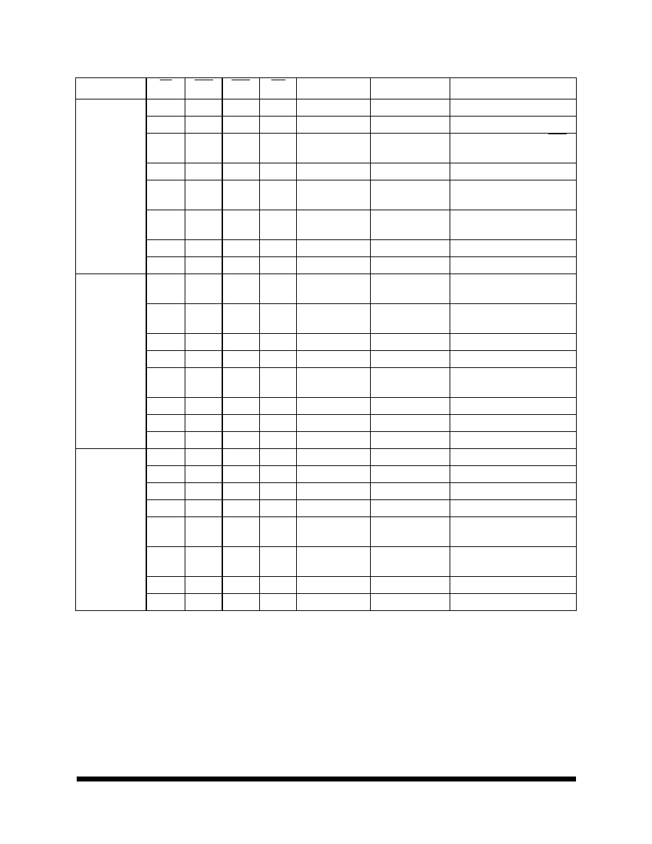
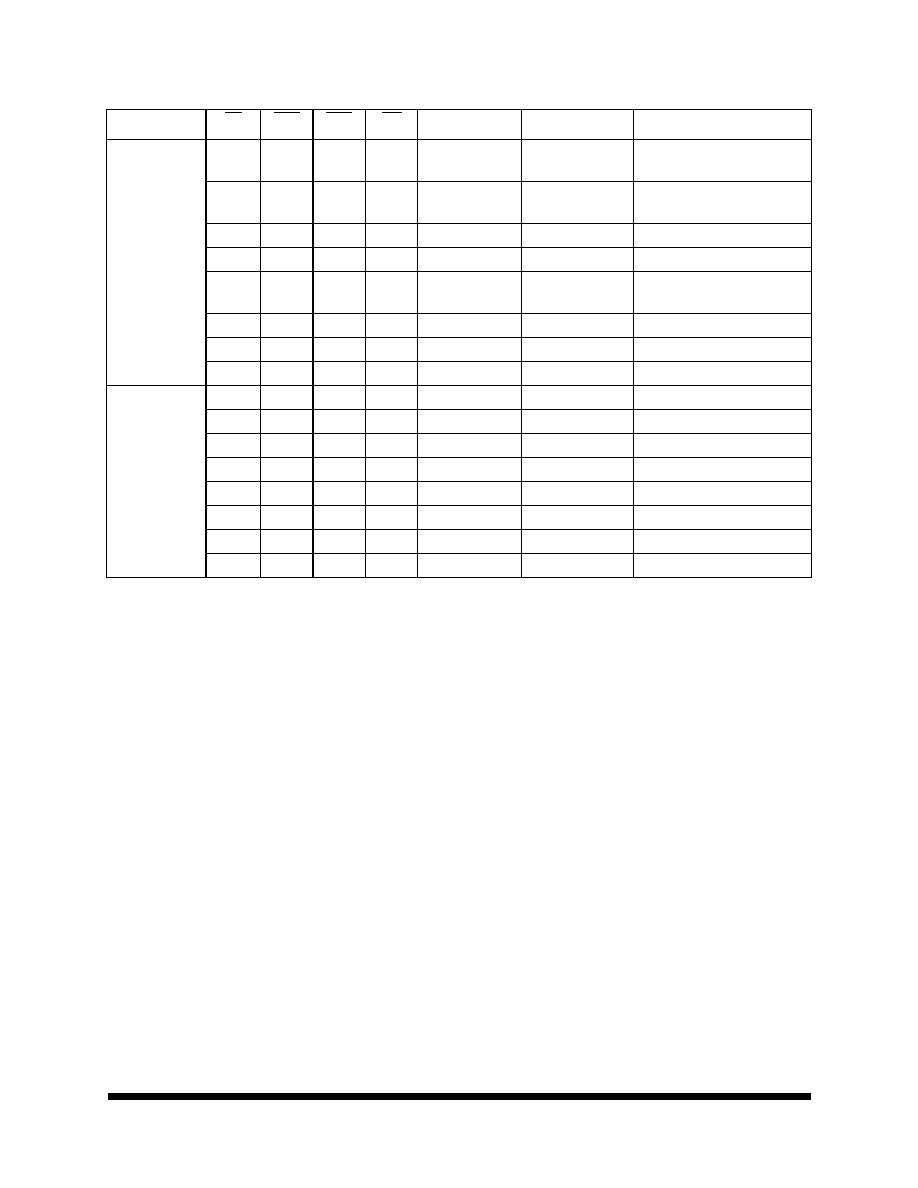
Function Truth Table
The following function table shows the operations that are performed when each command is issued in each
mode of the SDRAM.
The following table assumes that CKE is High.
C
URRENT
S
TATE
CS
RAS
CAS
WE
A
DDRESS
C
OMMAND
O
PERATION
Precharge
H
x
x
x
x
DESL
Enter IDLE after t
RP
L
H
H
H
x
NOP
Enter IDLE after t
RP
L
H
L
H
BA, CA, A10
READ/READ A
ILLEGAL
1
L
H
L
L
BA, CA, A10
WRIT/WRIT A
ILLEGAL
1
L
L
H
H
BA, RA
ACTV
ILLEGAL
1
L
L
H
L
BA, A10
PRE, PALL
NOP
2
L
L
L
H
x
REF, SELF
ILLEGAL
L
L
L
L
MODE
MRS
ILLEGAL
Idle
H
x
x
x
x
DESL
NOP
L
H
H
H
x
NOP
NOP
L
H
L
H
BA, CA, A10
READ/READ A
ILLEGAL
3
L
H
L
L
BA, CA, A10
WRIT/WRIT A
ILLEGAL
3
L
L
H
H
BA, RA
ACTV
Bank and row active
L
L
H
L
BA, A10
PRE, PALL
NOP
L
L
L
H
x
REF, SELF
Refresh
L
L
L
L
MODE
MRS
Mode register set
Row active
H
x
x
x
x
DESL
NOP
L
H
H
H
x
NOP
NOP
L
H
L
H
BA, CA, A10
READ/READ A
Begin read
L
H
L
L
BA, CA, A10
WRIT/WRIT A
Begin write
L
L
H
H
BA, RA
ACTV
Other bank active
ILLEGAL on same bank
4
L
L
H
L
BA, A10
PRE, PALL
Precharge
L
L
L
H
x
REF, SELF
ILLEGAL
L
L
L
L
MODE
MRS
ILLEGAL

97SD3240
M
e
m
o
r
y
13
All data sheets are subject to change without notice
©2005 Maxwell Technologies
All rights reserved.
1.25Gb (8-Meg X 40-Bit X 4-Banks) SDRAM
02.04.05 Rev 3
READ
H
x
x
x
x
DESL
Continue burst to end
L
H
H
H
x
NOP
Continue burst to end
L
H
L
H
BA, CA, A10
READ/READ A
Continue burst read to CAS
latency and new read
L
H
L
L
BA, CA, A10
WRIT/WRIT A
Term burst read/start write
L
L
H
H
BA, RA
ACTV
Other bank active
ILLEGAL on same bank
4
L
L
H
L
BA, A10
PRE, PALL
Term burst read and
Precharge
L
L
L
H
x
REF, SELF
ILLEGAL
L
L
L
L
MODE
MRS
ILLEGAL
Read with auto-
precharge
H
x
x
x
x
DESL
Continue burst to end and pre-
charge
L
H
H
H
x
NOP
Continue burst to end and pre-
charge
L
H
L
H
BA, CA, A10
READ/READ A
ILLEGAL
1
L
H
L
L
BA, CA, A10
WRIT/WRIT A
ILLEGAL
1
L
L
H
H
BA, RA
ACTV
Other bank active
ILLEGAL on same bank
4
L
L
H
L
BA, A10
PRE, PALL
ILLEGAL
1
L
L
L
H
x
REF, SELF
ILLEGAL
L
L
L
L
MODE
MRS
ILLEGAL
Write
H
x
x
x
x
DESL
Continue burst to end
L
H
H
H
x
NOP
Continue burst to end
L
H
L
H
BA, CA, A10
READ/READ A
Term burst and new read
L
H
L
L
BA, CA, A10
WRIT/WRIT A
Term burst and new write
L
L
H
H
BA, RA
ACTV
Other bank active
ILLEGAL on same bank
4
L
L
H
L
BA, A10
PRE, PALL
Term burst write and
precharge
5
L
L
L
H
x
REF, SELF
ILLEGAL
L
L
L
L
MODE
MRS
ILLEGAL
C
URRENT
S
TATE
CS
RAS
CAS
WE
A
DDRESS
C
OMMAND
O
PERATION

97SD3240
M
e
m
o
r
y
14
All data sheets are subject to change without notice
©2005 Maxwell Technologies
All rights reserved.
1.25Gb (8-Meg X 40-Bit X 4-Banks) SDRAM
02.04.05 Rev 3
From PRECHARGE state, command operation
To [DESL], [NOP]: When these commands are executed, the SDRAM enters the IDLE state after t
RP
has
elapsed from the completion of precharge.
From IDLE state, command operation
To [DESL], [NOP], [PRE], or [PALL]: These commands result in no operation.
To [ACTV]: The bank specified by the address pins and the ROW address is activated.
To [REF], [SELF]: The SDRAM enters refresh mode (auto-refresh or self-refresh).
To [MRS]: The synchronous DRAM enters the mode register set cycle.
From ROW ACTIVE state, command operation
To [DESL], [NOP]: These commands result in no operation.
To [READ], [READ A]: A read operation starts. (However, an interval of t
RCD
is required.)
To [WRIT], [WRIT A]: A write operation starts. (However, an interval of t
RCD
is required.)
Write with auto-
precharge
H
x
x
x
x
DESL
Continue burst to end and pre-
charge
L
H
H
H
x
NOP
Continue burst to end and pre-
charge
L
H
L
H
BA, CA, A10
READ/READ A
ILLEGAL
1
L
H
L
L
BA, CA, A10
WRIT/WRIT A
ILLEGAL
1
L
L
H
H
BA, RA
ACTV
Other bank active
ILLEGAL on same bank
4
L
L
H
L
BA, A10
PRE, PALL
ILLEGAL
1
L
L
L
H
x
REF, SELF
ILLEGAL
L
L
L
L
MODE
MRS
ILLEGAL
Refresh ( auto-
refresh)
H
x
x
x
x
DESL
Enter IDLE after t
RC
L
H
H
H
x
NOP
Enter IDLE after t
RC
L
H
L
H
BA, CA, A10
READ/READ A
ILLEGAL
3
L
H
L
L
BA, CA, A10
WRIT/WRIT A
ILLEGAL
3
L
L
H
H
BA, RA
ACTV
ILLEGAL
3
L
L
H
L
BA, A10
PRE, PALL
ILLEGAL
3
L
L
L
H
x
REF, SELF
ILLEGAL
L
L
L
L
MODE
MRS
ILLEGAL
1. Illegal for same bank, except for another bank
2. NOP for same bank, except for another bank
3. Illegal for all banks
4. If t
RRD
is not satisfied, this operation is illegal
5. An interval of t
DPL
is required between the final valid data input and the precharge command
C
URRENT
S
TATE
CS
RAS
CAS
WE
A
DDRESS
C
OMMAND
O
PERATION

97SD3240
M
e
m
o
r
y
15
All data sheets are subject to change without notice
©2005 Maxwell Technologies
All rights reserved.
1.25Gb (8-Meg X 40-Bit X 4-Banks) SDRAM
02.04.05 Rev 3
To [ACTV]: This command makes the other bank active. ( However, an interval of t
RRD
is required.)
Attempting to make the currently active bank active results in an illegal command.
To [PRE], [PALL]: These commands set the SDRAM to precharge mode. (However, an interval of t
RAS
is
required.)
From READ state, command operation
To [DESL], [NOP]: These commands continue read operations until the operation is completed.
To [READ], [READ A]: Data output by the previous read command continues to be output. After CAS
latency, the data output resulting from the next command will start.
To [WRIT], [WRIT A]: These commands stop a burst read, and start a write cycle.
To [ACTV]: This command makes other banks bank active. (However, an interval of t
RRD
is required.)
Attempting to make the currently active bank active results in an illegal command.
To [PRE], [PALL]: These commands stop a burst read, and the SDRAM enters precharge mode.
From READ with AUTO-PRECHARGE state, command operation
To [DESL], [NOP]: These commands continue read operations until the burst operation is completed, and
the SDRAM then enters precharge mode.
To [ACTV]: This command makes other banks active. (However, an interval of t
RRD
is required.) Attempting
to make the currently active bank active results in an illegal command.
From WRITE state, command operation
To [DESL], [NOP]: These commands continue write operations until the burst operation is completed.
To [READ], [READ A]: These commands stop a burst and start a read cycle.
To [WRIT], [WRIT A]: These commands stop a burst and start the next write cycle.
To [ACTV]: This command makes the other bank active. (However, an interval of t
RRD
is required.)
Attempting to make the currently active bank active results in an illegal command.
To [PRE], [PALL]: These commands stop burst write and the SDRAM then enters precharge mode.
From WRITE with AUTO-PRECHARGE state, command operation
To [DESL], [NOP]: These commands continue write operations until the burst is completed, and the
synchronous DRAM enters precharge mode.
To [ACTV]: This command makes the other bank active. (However, an interval of t
RRD
is required.)
Attempting to make the currently active bank active result in an illegal command.
From REFRESH state, command operation
To [DESL], [NOP]: After an auto-refresh cycle (after t
RC
) the SDRAM automatically enters the IDLE state.

97SD3240
M
e
m
o
r
y
16
All data sheets are subject to change without notice
©2005 Maxwell Technologies
All rights reserved.
1.25Gb (8-Meg X 40-Bit X 4-Banks) SDRAM
02.04.05 Rev 3
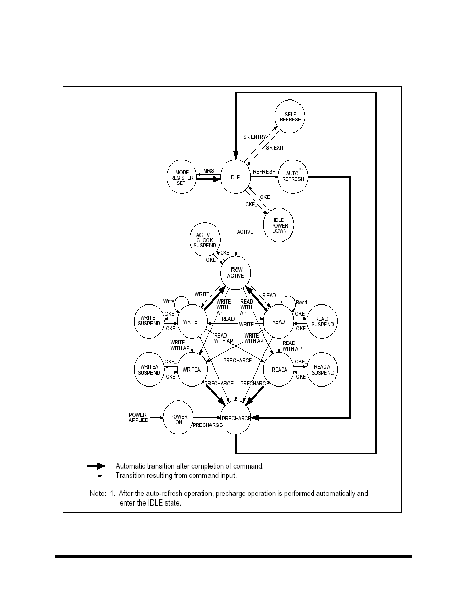
Simplified State Diagram

97SD3240
M
e
m
o
r
y
17
All data sheets are subject to change without notice
©2005 Maxwell Technologies
All rights reserved.
1.25Gb (8-Meg X 40-Bit X 4-Banks) SDRAM
02.04.05 Rev 3
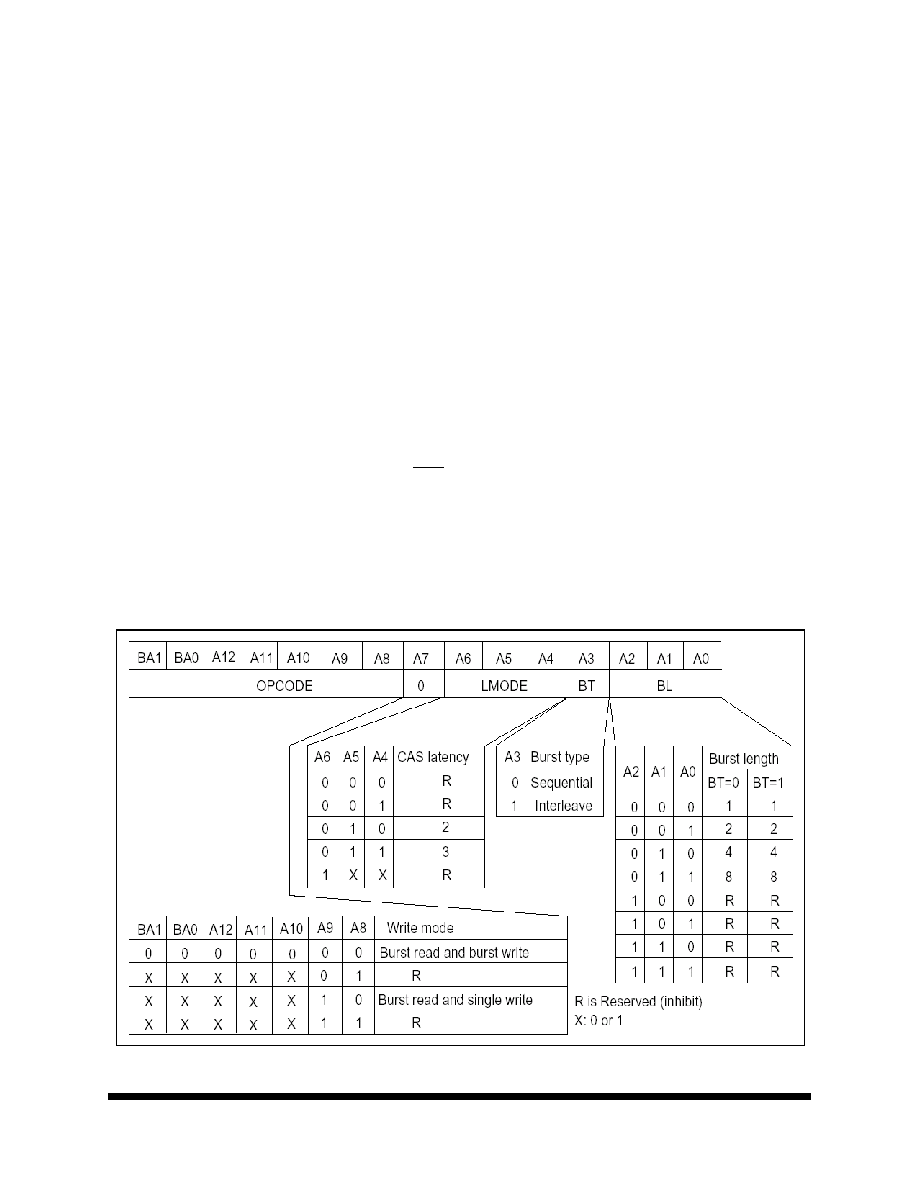
Mode Register Configuration
The mode register is set by the input to the address pins (A0 to A12, BA0 and BA1) during mode register set
cycles. The mode register consists of five sections, each of which is assigned to address pins.
BA0, BA1, A11, A10, A12, A9, A8: (OPCODE): The SDRAM has two types of write modes. One is the burst
write mode, and the other is the single write mode. These bits specify write mode.
Burst read and burst write: Burst write is performed for the specified burst length starting from the column
address specified in the write cycle.
Burst read and single write: Data is only written to the column address specified during the write cycle,
regardless of the burst length.
A7: Keep this bit Low at the mode register set cycle. If this pin is high, the vender test mode is set.
A6, A5, A4: (LMODE): These pins specify the CAS latency.
A3: (BT): A burst type is specified.
A2, A1, A0: (BL): These pins specify the burst length.

97SD3240
M
e
m
o
r
y
18
All data sheets are subject to change without notice
©2005 Maxwell Technologies
All rights reserved.
1.25Gb (8-Meg X 40-Bit X 4-Banks) SDRAM
02.04.05 Rev 3
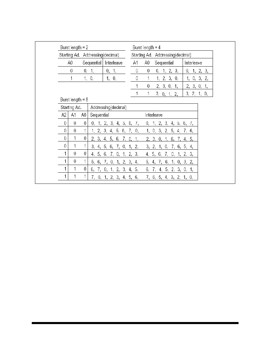
Burst Sequence

97SD3240
M
e
m
o
r
y
19
All data sheets are subject to change without notice
©2005 Maxwell Technologies
All rights reserved.
1.25Gb (8-Meg X 40-Bit X 4-Banks) SDRAM
02.04.05 Rev 3
Operation of the SDRAM
The following section shows operation examples of 97SD3240.
Note: The SDRAM should be used according to the product capability ( See Pin Description and AC
Characteristics.)
Read/Write Operations:
Bank Active: Before executing a read or write operation, the corresponding bank and the row address must
be activated by the bank active (ACTV) command. An interval of t
RCD
is required between the bank active
command input and the following read/write command input.
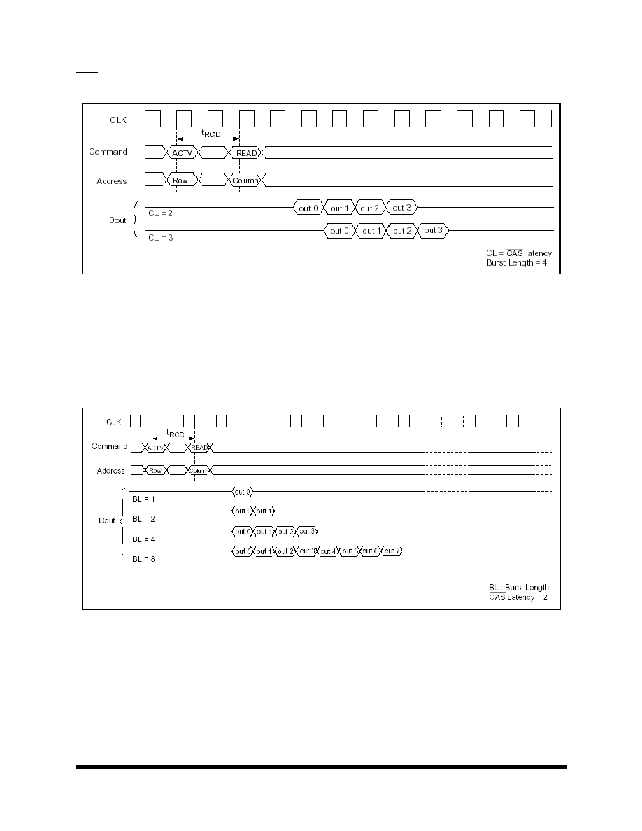
Read operation: A read operation starts when a read command is input. The output buffer becomes Low-Z
in the (CAS latency - 1) cycle after read command set. The SDRAM can perform a burst read operation.
The burst length can be set to 1, 2, 4, or 8. The start address for a burst read is specified by the column
address and the bank select address (BA0/BA1) at the read command set cycle. In a read operation, data
output starts after the number of clocks specified by the CAS latency. The CAS latency can be set to 2 or 3.
When the burst length is 1, 2, 4, or 8, the D
OUT
buffer automatically becomes High-Z at the next clock after
the successive burst-length data has been output.
The CAS latency and burst length must be specified at the mode register.

97SD3240
M
e
m
o
r
y
20
All data sheets are subject to change without notice
©2005 Maxwell Technologies
All rights reserved.
1.25Gb (8-Meg X 40-Bit X 4-Banks) SDRAM
02.04.05 Rev 3
CAS Latency
Burst Length

97SD3240
M
e
m
o
r
y
21
All data sheets are subject to change without notice
©2005 Maxwell Technologies
All rights reserved.
1.25Gb (8-Meg X 40-Bit X 4-Banks) SDRAM
02.04.05 Rev 3
Write Operation: Burst write or single write mode is selected by the OPCODE (BA1, BA0, A12, A11, A10,
A9, A8) of the mode register.
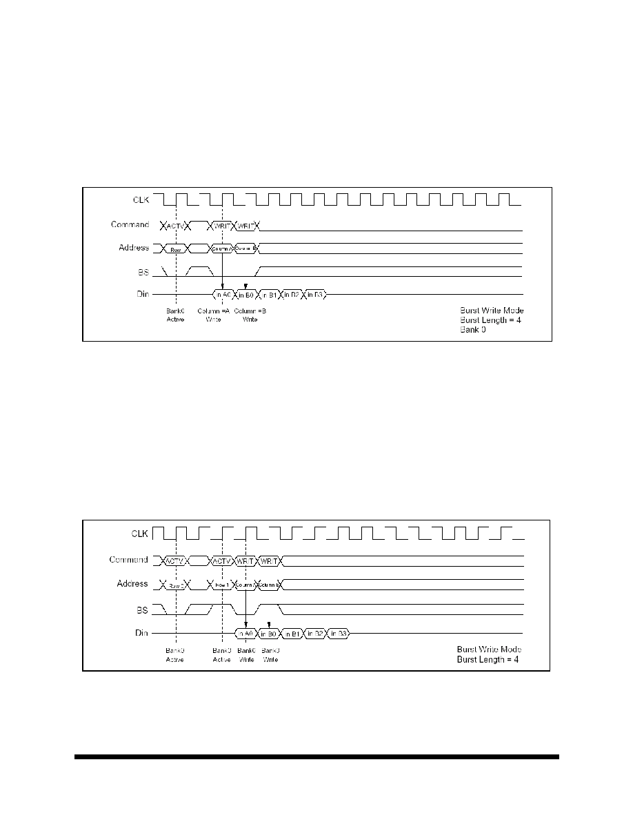
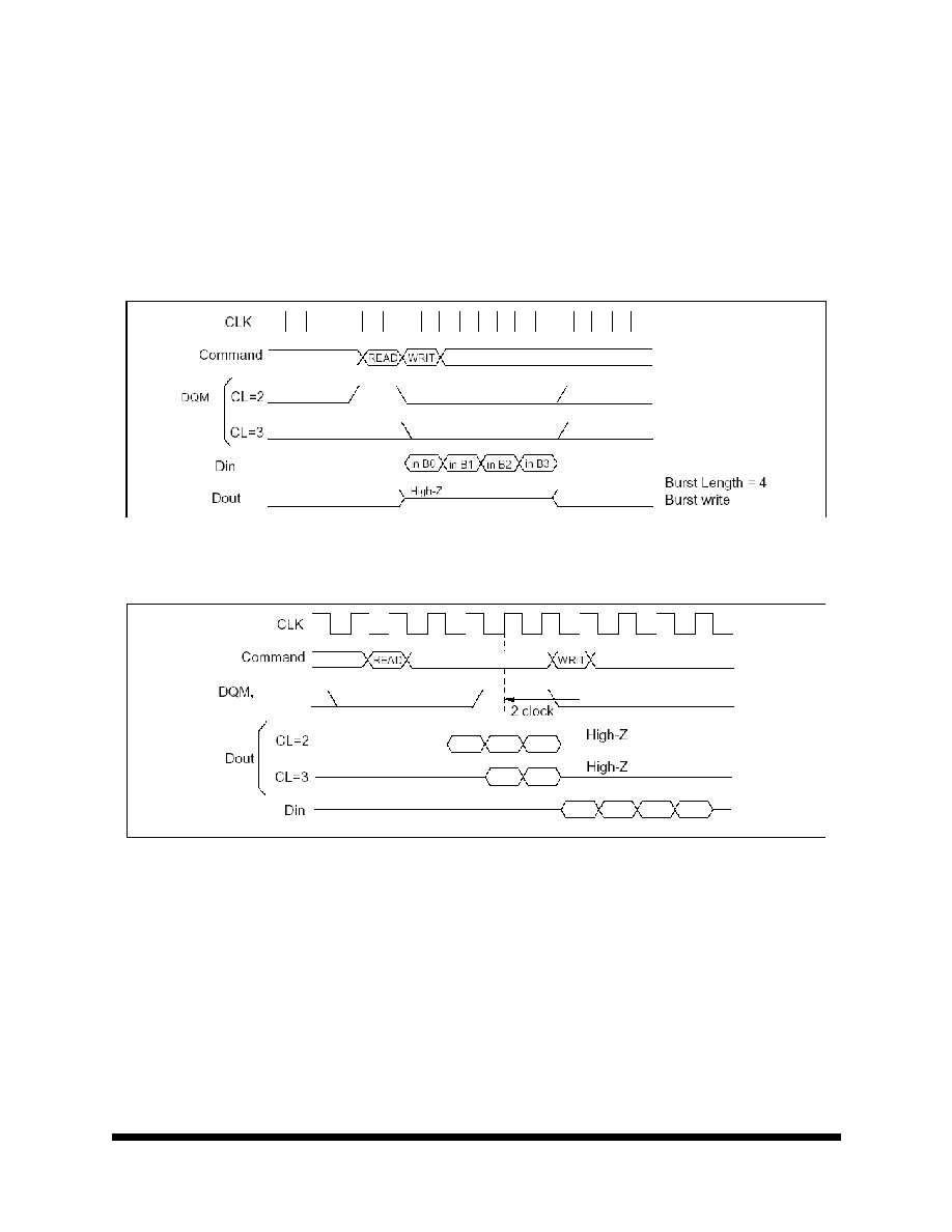
1. Burst write: A burst write operation is enabled by setting OPCODE (A9, A8) to (0, 0). A burst write starts
in the same clock as a write command set. (The latency of data input is 0 clock.) The burst length can be set
to 1, 2, 4, or 8, like burst read operations. The write start address is specified by the column address and the
bank select address (BA0/BA1) at the write command set cycle.
2. Single write: A single write operation is enabled by setting OPCODE ( A9, A8) to (1, 0). In a single write
operation, data is only written to the column address and the bank select address (BA0/BA1) specified by
the write command set cycle without regard to the burst length setting. ( The latency of data input is 0 clock.)

97SD3240
M
e
m
o
r
y
22
All data sheets are subject to change without notice
©2005 Maxwell Technologies
All rights reserved.
1.25Gb (8-Meg X 40-Bit X 4-Banks) SDRAM
02.04.05 Rev 3
Auto Precharge
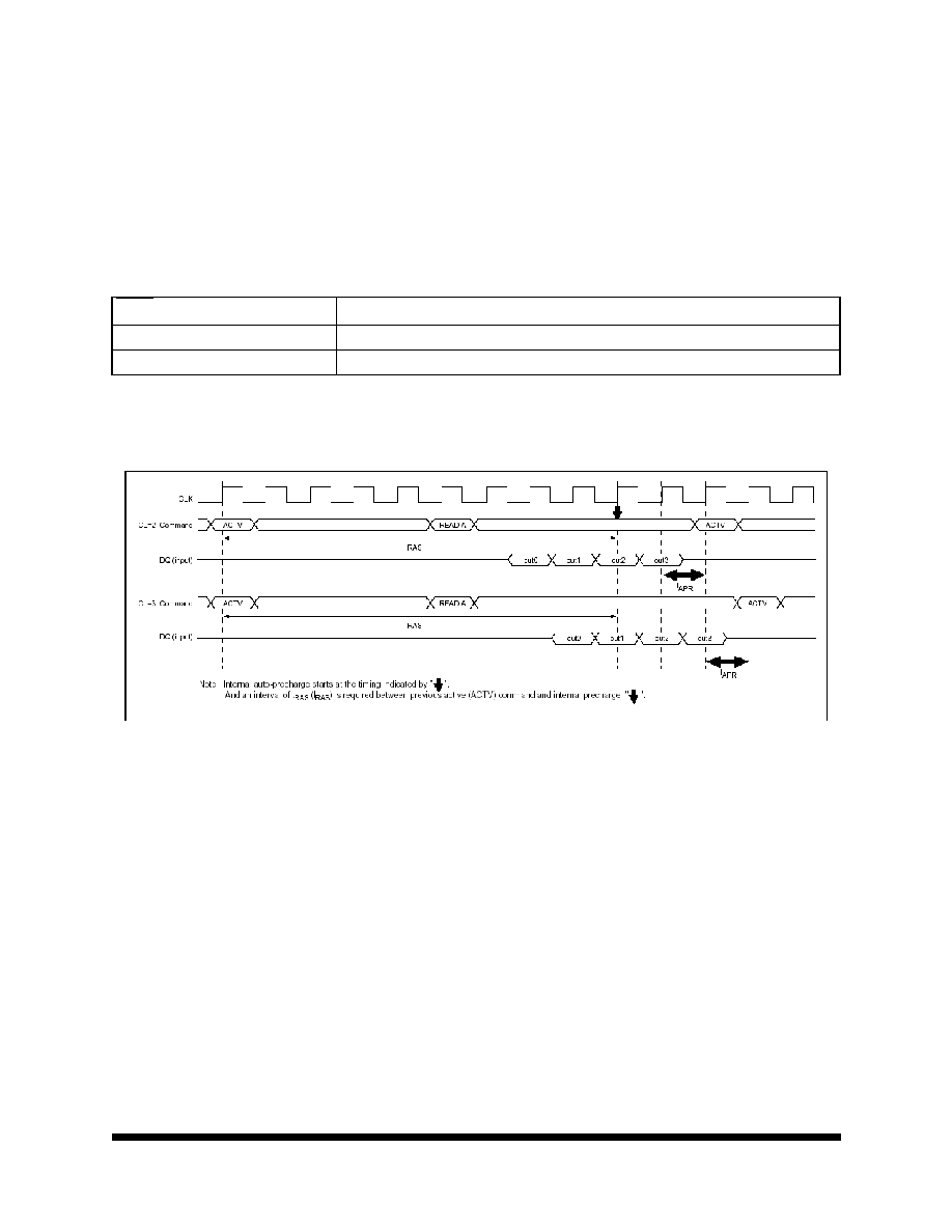
Read with auto-precharge: In this operation, since precharge is automatically performed after completing a
read operation, a precharge command need not be executed after each read operation. The command
executed for the same bank after the execution of this command must be the bank active (ACTV) command.
In addition, an interval defined by I
ARP
is required before execution of the next command.
Burst Read (Burst Length = 4)
CAS latency
Precharge start cycle
3
2 cycles before the final data is output
2
1 cycle before the final data is output

97SD3240
M
e
m
o
r
y
23
All data sheets are subject to change without notice
©2005 Maxwell Technologies
All rights reserved.
1.25Gb (8-Meg X 40-Bit X 4-Banks) SDRAM
02.04.05 Rev 3
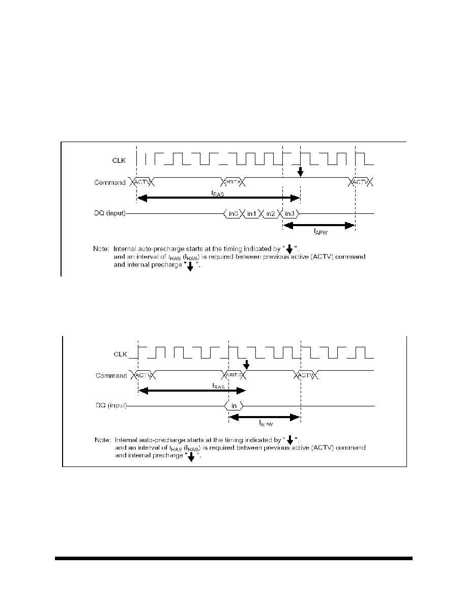
Write with auto-precharge: In this operation, since precharge is automatically preformed after completing a
burst write or single write operation, a precharge command need not be executed after each write operation.
The command executed for the same bank after the execution of this command must be the bank active
(ACTV) command. In addition, an interval of I
APW
is required between the final valid data input and input of
next command.
Burst Write (Burst Length = 4)
Single Write

97SD3240
M
e
m
o
r
y
24
All data sheets are subject to change without notice
©2005 Maxwell Technologies
All rights reserved.
1.25Gb (8-Meg X 40-Bit X 4-Banks) SDRAM
02.04.05 Rev 3
Command Intervals
READ command to READ command interval
1. Same bank, same ROW address: When another read command is executed at the same ROW address
of the same bank as the preceding read command execution, the second read can be performed after an
interval of no less than 1 clock. Even when the first command is a burst read that is not yet finished, the data
read by second command will be valid.
READ to READ Command Interval (Same ROW address in same bank)
2. Same bank, different ROW address: When the ROW address changes on the same bank, consecutive
read commands cannot be executed; it is necessary to separate the two read commands with a precharge
command and a bank-active command.
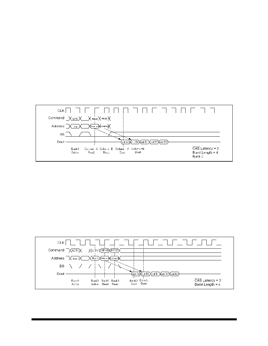
3. Different bank: When the bank changes, the second read can be performed after an interval of no less
than 1 clock, provided that the other bank is in the bank-active state. Even when the first command is a burst
read that is not yet finished, the data read by the second command will be valid.
READ to READ Command Interval ( Different Bank)

97SD3240
M
e
m
o
r
y
25
All data sheets are subject to change without notice
©2005 Maxwell Technologies
All rights reserved.
1.25Gb (8-Meg X 40-Bit X 4-Banks) SDRAM
02.04.05 Rev 3
Write command to Write command interval:
1. Same bank, same ROW address: When another write command is executed at the same ROW address
of the same bank as the preceding write command, the second write can be performed after as interval of no
less than 1 clock. In the case of burst writes, the second write command has priority.
Write to Write Command Interval (Same ROW address in same bank)
2. Same bank, different ROW address: When the ROW address changes, consecutive write commands
cannot be executed; it is necessary to separate the two write commands with a precharge command and a
bank-active command.
3. Different bank: When the bank changes, the second write can be performed after an interval of no less
than 1 clock, provided that the other bank is in the bank-active state. In the case of burst write, the second
write command has priority.
WRITE to WRITE Command Interval (Different bank)

97SD3240
M
e
m
o
r
y
26
All data sheets are subject to change without notice
©2005 Maxwell Technologies
All rights reserved.
1.25Gb (8-Meg X 40-Bit X 4-Banks) SDRAM
02.04.05 Rev 3
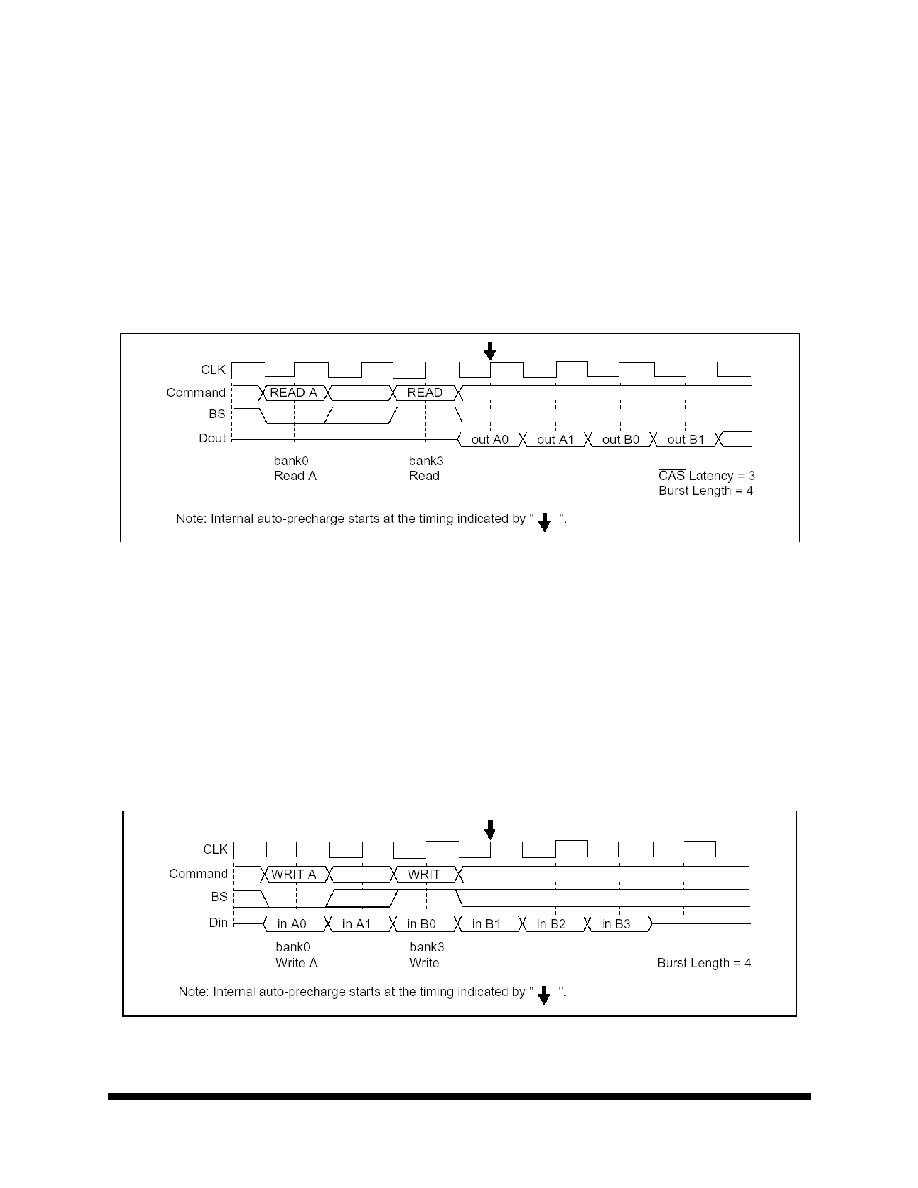
Read command to Write command Interval:
1. Same bank, same ROW address: When the write command is executed at the same ROW address of
the same bank as the preceding read command, the write command can be performed after an interval of no
less than 1 clock. However, DQM must be set High so the output buffer becomes High-Z before data input.
READ to WRITE Command Interval (1)
READ to WRITE Command Interval (2)
2. Same bank, different ROW address: When the ROW address changes, consecutive write commands
cannot be executed; it is necessary to separate the two commands with a precharge command and a bank-
active command.
3. Different bank: When the bank changes, the write command can be performed after an interval of no
less than 1 cycle, provided that the other bank is in the bank-active state. However, DQM must be set High
so that the output buffer becomes High-Z before data input.

97SD3240
M
e
m
o
r
y
27
All data sheets are subject to change without notice
©2005 Maxwell Technologies
All rights reserved.
1.25Gb (8-Meg X 40-Bit X 4-Banks) SDRAM
02.04.05 Rev 3
Write command to READ command interval:
1. Same bank, same ROW address: When the read command is executed at the same ROW address of
the same bank as the preceding write command, the read command can be performed after an interval of no
less than 1 clock. However, in the case of a burst write, data will continue to be written until one clock before
the read command is executed.
WRITE to READ Command Interval (1)
Write to READ Command Interval (2)
2. Same bank, different ROW address: When the ROW address changes, consecutive read commands
cannot be executed; it is necessary to separate the two commands with a precharge command and a bank-
active command.
3. Different bank: When the bank changes, the read command can be performed after an interval of no less
than 1 clock, provided that the other bank is in the bank-active state. However, in the case of a burst write,
data will continue to be written until one clock before the read command is executed (as in the case of the
same bank and the same address).

97SD3240
M
e
m
o
r
y
28
All data sheets are subject to change without notice
©2005 Maxwell Technologies
All rights reserved.
1.25Gb (8-Meg X 40-Bit X 4-Banks) SDRAM
02.04.05 Rev 3
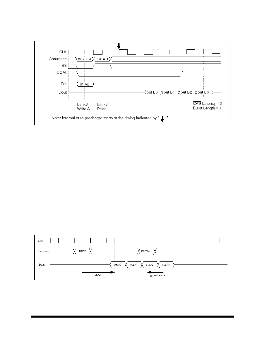
Read with Auto Precharge to READ command interval
1. Different bank: When some banks are in the active state, the second read command ( another bank) is
executed. Even when the first read with auto-precharge is a burst read that is not yet finished, the data read
by the second command is valid. The interval auto-precharge of one bank starts at the next clock of the
second command.
Read with Auto Precharge to Read Command Interval (Different Bank)
2. Same Bank: The consecutive read command (the same bank) is illegal.
Write with Auto Precharge to Write command interval
1. Different bank: When some banks are in the active state, the second write command (another bank) is
executed. In the case of burst writes, the second write command has priority. The internal auto-precharge of
one bank starts at the next clock of the second command.
Write with Auto Precharge to Write Command Interval (Different bank)

97SD3240
M
e
m
o
r
y
29
All data sheets are subject to change without notice
©2005 Maxwell Technologies
All rights reserved.
1.25Gb (8-Meg X 40-Bit X 4-Banks) SDRAM
02.04.05 Rev 3
2. Same bank: The consecutive write command ( the same bank) is illegal.
Read with Auto Precharge to Write command interval
1. Different bank: When some banks are in the active state, the second write command (another bank) is
executed. However, DQM must be set High so that the output buffer becomes High-Z before data input. The
internal auto-precharge of one bank starts at the next clock of the second command.
Read with Auto Precharge to Write Command Interval (Different bank)
2. Same bank: The consecutive write command from read with auto precharge ( the same bank) is illegal. It
is necessary to separate the two commands with a bank active command.
Write with Auto Precharege to Read command interval
1. Different bank: When some banks are in the active state, the second read command (another bank) is
executed. However, in the case of a burst write, data will continue to be written until one clock before the
read command is executed. The internal auto precharge of one bank starts at the next clock of the second
command.
Write with Auto Precharge to Read command Interval (Different bank)

97SD3240
M
e
m
o
r
y
30
All data sheets are subject to change without notice
©2005 Maxwell Technologies
All rights reserved.
1.25Gb (8-Meg X 40-Bit X 4-Banks) SDRAM
02.04.05 Rev 3
2. Same Bank: The consecutive read command from write with auto precharge (the same bank) is illegal. It
is necessary to separate the two commands with a bank active command.
Read command to Precharge command Interval (same bank)
When the precharge command is executed for the same bank as the read command that preceded it, the
minimum interval between the two commands is one clock. However, since the output buffer than becomes
High-Z after the clock defined by I
HZP
, there is a case of interruption to burst read data. Output will be
interrupted if the precharge command is input during burst read. To read all data by burst read, the clocks
defined by I
EP
must be assured as an interval from the final data output to precharge command execution.
READ to PRECHARGE command Interval (same bank: To output all data)
CAS Latency = 2, Burst Length = 4
CAS Latency = 3, Burst Length = 4

97SD3240
M
e
m
o
r
y
31
All data sheets are subject to change without notice
©2005 Maxwell Technologies
All rights reserved.
1.25Gb (8-Meg X 40-Bit X 4-Banks) SDRAM
02.04.05 Rev 3
Recharge command Interval (same bank): To stop output data
CAS Latency = 2, Burst Length = 1, 2, 4, 8
CAS Latency = 3, Burst Length = 1, 2, 4, 8
d to Precharge command interval (same bank): When the precharge command is executed for the same
bank as the write command that preceded it, the minimum interval between the two commands is 1 clock.
However, if the burst write operation is unfinished, the data must be masked by means of DQM for
assurance of the clock defined by t
DPL
.
WRITE to PRECHARGE Command Interval (same bank)
Burst Length = 4 (To stop write operation)

97SD3240
M
e
m
o
r
y
32
All data sheets are subject to change without notice
©2005 Maxwell Technologies
All rights reserved.
1.25Gb (8-Meg X 40-Bit X 4-Banks) SDRAM
02.04.05 Rev 3
Burst Length = 4 (To write to all data)
Bank active command interval:
1. Same bank: The interval between the two bank-active commands must be no less than t
RC
.
2. In the case of different bank-active commands: The interval between the two bank-active commands
must be no less than t
RRD
.

97SD3240
M
e
m
o
r
y
33
All data sheets are subject to change without notice
©2005 Maxwell Technologies
All rights reserved.
1.25Gb (8-Meg X 40-Bit X 4-Banks) SDRAM
02.04.05 Rev 3
Bank Active to Bank Active for Same Bank
Bank Active to Bank Active for Different Bank

97SD3240
M
e
m
o
r
y
34
All data sheets are subject to change without notice
©2005 Maxwell Technologies
All rights reserved.
1.25Gb (8-Meg X 40-Bit X 4-Banks) SDRAM
02.04.05 Rev 3
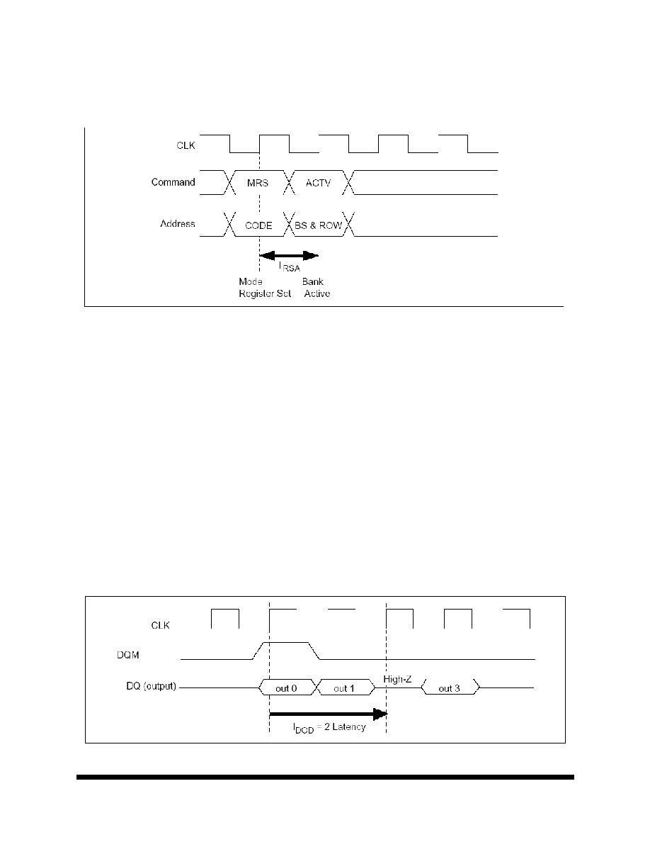
Mode register set to Bank-active interval: The interval between setting the mode register and executing a
bank-active command must be no less than I
RSA
.
DQM Control
The DQM mask the bytes of the DQ data. The timing of DQM is different during reading and writing.
Reading: When data is read, the output buffer can be controlled by DQM. By setting DQM to Low, the output
buffer becomes Low-Z, enabling data output. By setting DQM to High, the output buffer becomes High-Z and
the corresponding data is not output. However, internal reading operations continue. The latency of DQM
during reading is 2 clocks.
Writing: Input data can be masked by DQM. By setting DQM to Low, data can be written. In addition, when
DQM is set to High, the corresponding data is not written, and previous data is held. The latency of DQM
during writing is 0 clock.
Reading

97SD3240
M
e
m
o
r
y
35
All data sheets are subject to change without notice
©2005 Maxwell Technologies
All rights reserved.
1.25Gb (8-Meg X 40-Bit X 4-Banks) SDRAM
02.04.05 Rev 3
Writing
Refresh
Auto-Refresh: All the banks must be precharged before executing an auto-refresh command. Since the
auto-refresh command updates the internal counter every time it is executed and determines the banks and
the ROW addresses to be refreshed, external address specification is not required. The refresh cycle is
8192 cycles/6.4 ms. (8192 cycles are requires to refresh all the ROW addresses.) The output buffer
becomes High-Z after auto-refresh start. In addition, since a precharge has been completed by an internal
operation after the auto-refresh, an additional precharge operation by the precharge command is not
required.
Self-refresh
1
: After executing a self-refresh command, the self-refresh operation continues while CKE is
held Low. During self-refresh operation, all ROW addresses are refreshed by the internal refresh timer. A
self-refresh is terminated by a self-refresh exit command. Before and after self-refresh mode, execute auto-
refresh to all refresh addresses in or within 6.4ms period on the condition (1) and (2) below.
(1) Enter self-refresh mode within 7.8 us after either burst refresh or distributed refresh at equal interval until
all refresh addresses are completed.
(2) Start burst refresh or distributed refresh at equal interval to all refresh addreses within 7.8 us after exiting
from self-refresh mode.
Others
Power-down mode: The SDRAM enters power-down mode when CKE goes Low in the IDLE state. In
power-down mode, power consumption is suppressed by deactivating the input initial circuit. Power-down
mode continues while CKE is held Low. In addition, by setting CKE to High, the SDRAM exits from the
1. Self refresh mode should only be used at temperatures below 70∞C.

97SD3240
M
e
m
o
r
y
36
All data sheets are subject to change without notice
©2005 Maxwell Technologies
All rights reserved.
1.25Gb (8-Meg X 40-Bit X 4-Banks) SDRAM
02.04.05 Rev 3
power-down mode, and command input is enabled from the next clock. In this mode, internal refresh is not
performed.
Clock suspend mode: By driving CKE to Low during a bank-active or read/write operation, the SDRAM
enters clock suspend mode. During clock suspend mode, external input signals are ignored and the internal
state is maintained. When CKE is driven High, the SDRAM terminates clock suspend mode, and command
input is enabled from the next clock. For more details, refer to the "CKE Truth Table".
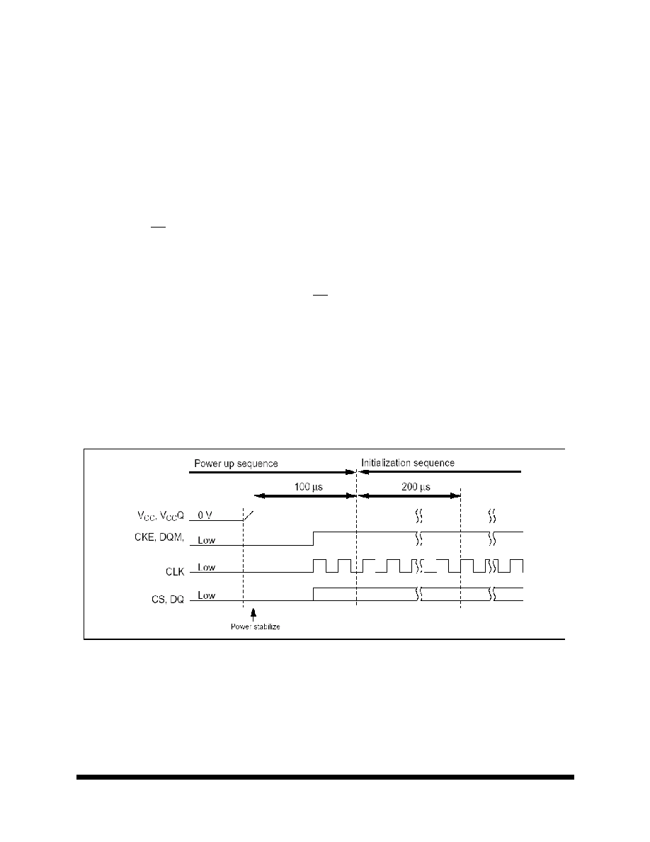
Power-up sequence: The SDRAM should use the following sequence during power-up:
The CLK, CKE, CS, DQM and DQ pins stay low until power stabilizes.
The CLK pin is stable within 100ms after power stabilizes before the following initialization sequence.
The CKE and DQM is driven high between when power stabilizes and the initialization sequence.
This SDRAM has V
CC
clamp diodes for CLK, CKE, CS, DQM and DQ pins. If these pins go high before
power up, the large current flows from these pins to V
CC
through
the diodes.
Initialization sequence: When 200ms or more has past after the power up sequence, all banks must be
precharged using the precharge command (PALL). After t
RP
delay, set 8 or more auto refresh commands
(REF). Set the mode register set command (MRS) to initialize the mode register. It is recommended that by
keeping DQM and CKE High, the output buffer becomes High-Z during initialization sequence, to avoid DQ
bus contention on a memory system formed with a number of devices.

97SD3240
M
e
m
o
r
y
37
All data sheets are subject to change without notice
©2005 Maxwell Technologies
All rights reserved.
1.25Gb (8-Meg X 40-Bit X 4-Banks) SDRAM
02.04.05 Rev 3
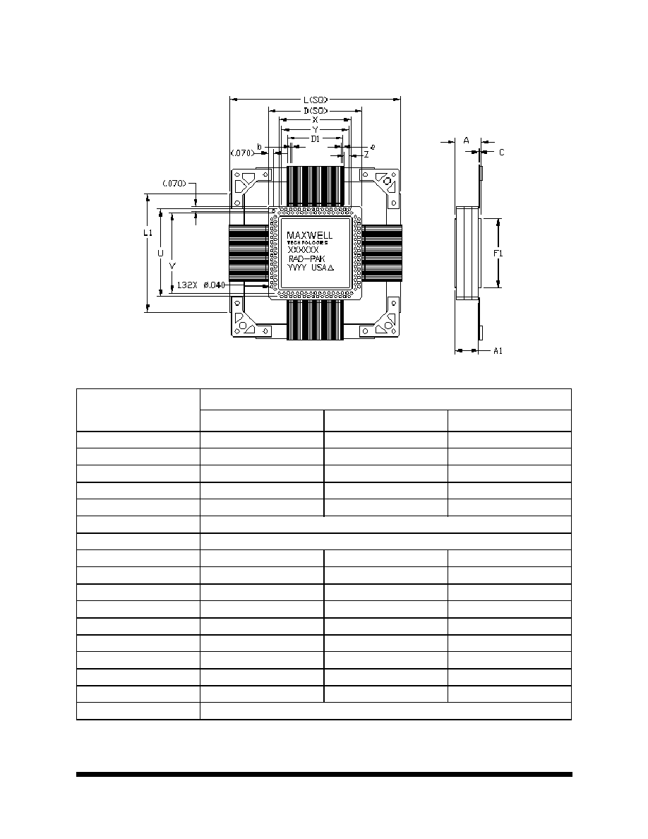
Note: All dimensions in inches.
132-L
EAD
Q
UAD
R
AD
-S
TACK
P
ACKAGE
S
YMBOL
D
IMENSION
(
INCHES
)
MIN
NOM
MAX
A
.385
.398
.411
b
.006
.008
.010
c
.005
.006
.008
D
1.337
1.350
1.363
D1
.795
.800
.805
e
.025
S1
.266
F1
.997
1.000
1.003
L
2.485
2.500
2.505
L1
1.685
1.700
1.715
A1
.355
.368
.381
X
1.030
1.040
1.050
Y
.965
.975
.985
Z
.060
.065
.070
U
1.160
1.260
1.360
V
1.160
1.160
1.360
N
132

97SD3240
M
e
m
o
r
y
38
All data sheets are subject to change without notice
©2005 Maxwell Technologies
All rights reserved.
1.25Gb (8-Meg X 40-Bit X 4-Banks) SDRAM
02.04.05 Rev 3
Important Notice:
These data sheets are created using the chip manufacturer's published specifications. Maxwell Technologies verifies
functionality by testing key parameters either by 100% testing, sample testing or characterization.
The specifications presented within these data sheets represent the latest and most accurate information available to
date. However, these specifications are subject to change without notice and Maxwell Technologies assumes no
responsibility for the use of this information.
Maxwell Technologies' products are not authorized for use as critical components in life support devices or systems
without express written approval from Maxwell Technologies.
Any claim against Maxwell Technologies must be made within 90 days from the date of shipment from Maxwell
Techoogies. Maxwell Technologies' liability shall be limited to replacement of defective parts.

97SD3240
M
e
m
o
r
y
39
All data sheets are subject to change without notice
©2005 Maxwell Technologies
All rights reserved.
1.25Gb (8-Meg X 40-Bit X 4-Banks) SDRAM
02.04.05 Rev 3
P
RODUCT
O
RDERING
O
PTIONS
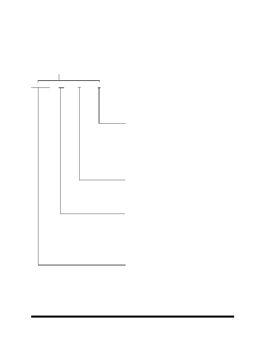
Model Number
Feature
Option Details
97SD3240
RP
Q
X
Screening Flow
Package
Radiation Feature
Base Product
Nomenclature
MCM
1
K = Maxwell Self-Defined Class K
H = Maxwell Self-Defined Class H
I = Industrial (testing @ -55∞C,
+25∞C, +125∞C)
E = Engineering (testing @ +25∞C)
Q = Quad Flat Package
RP = R
AD
-P
AK
Æ package
1.25Gb(8-Meg X 40-Bit X 4-
Banks) SDRAM
1) Products are manufactured and screened to Maxwell Technologies self-defined Class H and Class K flows.

