1
M
e
m
o
r
y
All data sheets are subject to change without notice
(858) 503-3300 - Fax: (858) 503-3301 - www.maxwell.com
Operational Amplifiers
OP284
©2003 Maxwell Technologies
All rights reserved.
07.25.03 Rev 3
F
EATURES
:
∑ R
AD
-P
AK
Æ radiation-hardened against natural space radia-
tion
∑ Total dose hardness:
- > 100 krad (Si), depending upon space mission
∑ Package:
- 8-pin R
AD
-P
AK
Æ flat pack
- 16-pin R
AD
-P
AK
Æ Leadless Chip Carrier (LCC) pack
∑ Single-Supply Operation
∑ Wide Bandwidth: 4 MHz
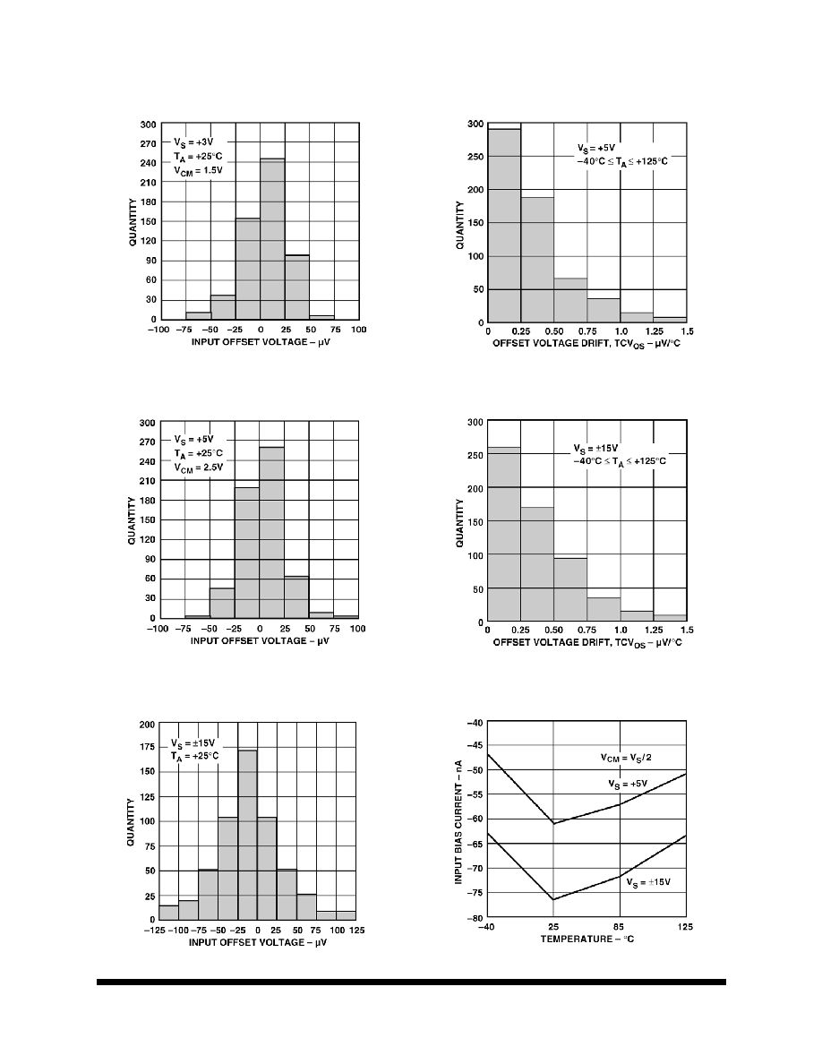
∑ Low Offset Voltage: 65uV
∑ Unity-Gain Stable
∑ High Slew Rate: 4.0 V/ms
∑ Low Noise: 3.9 nV/(Hz)
Ω
D
ESCRIPTION
:
Maxwell Technologies
' OP284 is a dual single-supply, 4
MHz bandwidth amplifier featuring rail-to-rail inputs and out-
puts and a greater than 100 krad (Si) total dose tolerance,
depending upon space mission. Using
Maxwell Technolo-
gies
' radiation-hardened R
AD
-P
AK
Æ technology, it is guaran-
teed to operate from +3 to +36 (or ±1.5 to ±18) volts and will
function with a single supply as low as +1.5 volts.
This amplifier is superb for single supply applications requiring
both ac and precision dc performance. The combination of
bandwidth, low noise and precision makes the OP284 useful
in a wide variety of applications, including filters and instru-
mentation. Other applications for this amplifier include porta-
ble telecom equipment, power supply control and protection,
and as an amplifier or buffer for transducers with wide output
ranges.
The ability to swing rail-to-rail at both the input and output
enables designers to build multi-stage filters in single-supply
systems and to maintain high signal-to-noise ratios.
Maxwell Technologies' patented R
AD
-P
AK
Æ packaging technol-
ogy incorporates radiation shielding in the microcircuit pack-
age. It eliminates the need for box shielding while providing
the required radiation shielding for a lifetime in orbit or space
mission. In a GEO orbit, R
AD
-P
AK
Æ provides greater than 100
krad (Si) radiation dose tolerance. This product is available
with screening up to Class S.
Q1
Q3
QL1
QL2
Q4
Q2
R4
QB6
QB5
Q7
Q5
Q9
Q11
Q8
Q6
Q12
Q10
R6
QB9
RB3
QB10
RB4
CFF
CC2
Q16
Q17
R11
CO
Q18
R3
QB3
RB2
R7
Q13
Q14
R9
Q15
R1
R2
QB4
CC1
QB7
QB8
R8
R10
R5
RB1
JB1
QB2
CB1
M
N+
P+
QB1
JB2
-IN
+IN
OUT
V
CC
V
EE
TP
Logic Diagram
Flat Pack
Leadless Chip Carrier (LCC)
M
e
m
o
r
y
2
All data sheets are subject to change without notice
©2003 Maxwell Technologies
All rights reserved.
Operational Amplifiers
OP284
07.25.03 Rev 3
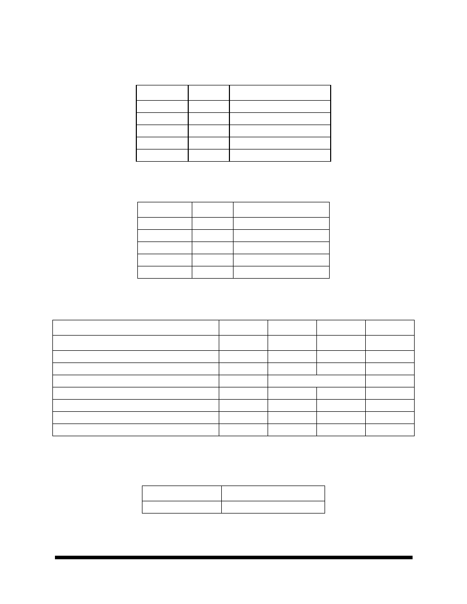
T
ABLE
1. F
LAT
P
ACK
P
INOUT
D
ESCRIPTION
P
IN
S
YMBOL
D
ESCRIPTION
1, 7
OUT A, B
Outputs
2, 6
-IN A, B
Negative Inputs
3, 5
+IN A, B
Positive Inputs
4
V-
Ground
8
V+
Supply Voltage
T
ABLE
2. L
EADLESS
C
HIP
C
ARRIER
(LCC) P
INOUT
D
ESCRIPTION
P
IN
S
YMBOL
D
ESCRIPTION
1, 13
OUT A, B
Outputs
3, 11
-IN A, B
Negative Inputs
5, 9
+IN A, B
Positive Inputs
7
V-
Ground
15
V+
Supply Voltage
T
ABLE
3. OP284 A
BSOLUTE
M
AXIMUM
R
ATINGS
P
ARAMETER
S
YMBOL
M
IN
M
AX
U
NIT
Supply Voltage
V
CC
--
±18
V
Input Voltage
V
I
--
±18
V
Differential Input Voltage
1
1. For input voltages greater than 0.6 volts, the input current should be limited to less 5 mA to prevent degradation or destruction of
the input devices.
V
DIF
--
±0.6
V
Output Short-Circuit Duration to GND
Indefinite
Storage Temperature Range
T
S
-65
+150
∞C
Operating Temperature Range
T
A
-40
+125
∞C
Junction Temperature Range
T
J
-65
+150
∞C
Thermal Impedance
JC
--
6.48
∞C/W
T
ABLE
4. D
ELTA
L
IMITS
P
ARAMETER
V
ARIATION
I
CC
±10% of specified value in Table 5
M
e
m
o
r
y
3
All data sheets are subject to change without notice
©2003 Maxwell Technologies
All rights reserved.
Operational Amplifiers
OP284
07.25.03 Rev 3
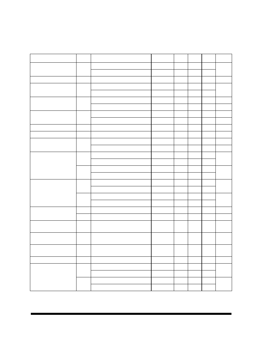
T
ABLE
5. OP284 E
LECTRICAL
C
HARACTERISTICS
(V+ = 15V, V- = -15V, V
OUT
= 0V, R
S
= 50
, R
L
= 100
K
, V
CM
= 0V, T
A
= -40∞C
TO
+125∞C
UNLESS
OTHERWISE
SPECIFIED
.)
P
ARAMETER
S
YMBOL
T
EST
C
ONDITIONS
S
UBGROUPS
M
IN
T
YP
M
AX
U
NIT
Input offset voltage
V
IO
+25∞C
1
-100
--
100
µ V
-40 to +125∞C
2, 3
-200
--
200
Average offset voltage drift
1
V
IO
TC R
L
=2k
1, 2, 3
--
--
2
µ V/∞C
Offset voltage match
1
V
IO
|V
IO
(max) - V
IO
(min)|, +25∞C
1
-
--
100
µ V
|V
IO
(max) - V
IO
(min)|, -40 to +125∞C
2, 3
-
--
200
Input bias current
I
B
R
S
= 50
, +25∞C
1
-350
--
350
nA
R
S
= 50
, -40 to +125∞C
2, 3
-575
--
575
nA
Input offset current
I
OS
R
S
=50
, +25∞C
1
-35
--
35
nA
R
S
= 50
, -40 to +125∞C
2, 3
-50
--
50
nA
Input bias current drift
1
I
IBTC
R
S
= 50
1, 2, 3
--
200
pA/∞C
Input voltage range
I
VR
1, 2, 3
-15
--
15
V
Common mode rejection
ratio
CMRR V
CM
= -14V to +14V
1, 2, 3
86
--
--
dB
V
CM
= -15V to +15V, T
A
=25∞C
1
80
--
--
dB
Output current
+I
O
V
OUT
= -10V, 1ms pulse, T
A
=25∞C
1
10
--
--
mA
V
OUT
= -10V, 1ms pulse
2, 3
5
--
--
-I
O
V
OUT
= +10V, 1ms pulse, T
A
=25∞C
1
--
-10
mA
V
OUT
= -10V, 1ms pulse
2, 3
--
-5
Quiescent power supply
current/amplifier
+I
CC
I
OUT
= 0mA V
S
=±18V, T
A
=25∞C
1
--
--
1.80
mA
I
OUT
= 0mA V
S
=±18V
2, 3
--
--
2.25
-I
CC
I
OUT
= 0mA V
S
=±18V, T
A
=25∞C
1
-1.80
--
--
mA
I
OUT
= 0mA V
S
=±18V
2, 3
2.25
--
--
Power supply rejection ratio +PSRR V
S
=±2V to ±18V
1, 2, 3
90
--
--
dB
-PSRR V
S
=±2V to ±18V
1, 2, 3
90
--
--
dB
Low frequency, peak-to-
peak noise
1
E
np-p
0.1Hz to 10Hz, R
L
=2k
,
C
L
=50pF, T
A
=+25∞C
1
--
0.30
--
µ V
p-p
Input noise voltage density
1
E
n
R
S
=20
, f
O
=1kHz, R
L
=2k
,
C
L
=50pF, T
A
=+25∞C
1
--
3.9
--
nV/
(Hz)
Ω
Input noise current density
1
I
n
R
S
=20M
, f
O
=1kHz, R
L
=2k
,
C
L
=50pF, T
A
=+25∞C
1
--
0.4
--
pA/
(Hz)
Ω
Power consumption
1,2
P
C
+10V, I
OUT
=0mA, R
L
=2k
1, 2, 3
--
81
mW
Large signal voltage gain
+A
VOL
+10V, R
L
=2.0k
,T
A
=25∞C
1
--
150
V/mV
+10V, R
L
=2.0k
2, 3
75
-A
VOL
-10V, R
L
=2.0k
,T
A
=25∞C
1
--
150
V/mV
-10V, R
L
=2.0k
2, 3
75

M
e
m
o
r
y
4
All data sheets are subject to change without notice
©2003 Maxwell Technologies
All rights reserved.
Operational Amplifiers
OP284
07.25.03 Rev 3
Output voltage swing
+V
OUT1
I
L
=1.0mA
1, 2, 3
14.8
--
--
V
-V
OUT1
I
L
=1.0mA
1, 2, 3
--
--
-14.8
V
Gain bandwidth product
1
GBWP V
O
=200mV, R
L
=2.0k
,
C
L
=50pF, T
A
=+25∞C
1
--
4.25
--
MHz
Full power bandwidth
1,3
FPBW V
PEAK
=29vp-p, R
L
=2.0k
,
C
L
=50pF, T
A
=+25∞C, 1% distortion
1
--
35
--
kHz
Settling time
t
S
A
V
=+1.0, C
L
=50pF, R
L
=2.0k
To 0.01%, 10V step
1, 2, 3
--
--
5
µ s
Phase margin
F
O
AV=1.0, C
L
=50pF,
R
L
=2.0k
, T
A
=+25∞C
1
--
--
50
Degrees
Slew rate
+SR
C
L
=50pF, R
L
=2.0k
1, 2, 3
--
--
2.4
V/µ s
-SR
C
L
=50pF, R
L
=2.0k
1, 2, 3
--
--
2.4
V/µ s
1. Guaranteed by design.
2. Power consumption is based upon quiescent supply current maximum test limit. No load on outputs.
3. Full power bandwidth is based on slew rate measurement using FBBW = slew rate/(2
P
V
PEAK
).
T
ABLE
5. OP284 E
LECTRICAL
C
HARACTERISTICS
(V+ = 15V, V- = -15V, V
OUT
= 0V, R
S
= 50
, R
L
= 100
K
, V
CM
= 0V, T
A
= -40∞C
TO
+125∞C
UNLESS
OTHERWISE
SPECIFIED
.)
P
ARAMETER
S
YMBOL
T
EST
C
ONDITIONS
S
UBGROUPS
M
IN
T
YP
M
AX
U
NIT