 | –≠–ª–µ–∫—Ç—Ä–æ–Ω–Ω—ã–π –∫–æ–º–ø–æ–Ω–µ–Ω—Ç: OP490RPFE | –°–∫–∞—á–∞—Ç—å:  PDF PDF  ZIP ZIP |

1
Memory
All data sheets are subject to change without notice
(858) 503-3300 - Fax: (858) 503-3301 - www.maxwell.com
Low Voltage Micropower Quad
©2001 Maxwell Technologies
All rights reserved.
OP490
Operational Amplifier
12.19.01 Rev2
1000560
F
EATURES
:
∑ R
AD
-P
AK
Æ technology-hardened against natural space radi-
ation
∑ Package:
- 16 pin Rad-PakÆ flat package
∑ Low input offset voltage: 5 µV max
∑ Low offset voltage drift
- 5 µV/∞C max (over -55 to +125∞C)
∑ Low supply current (per amplifier) 20 µA max
∑ High open-loop gain 700 V/me min.
∑ Outstanding PSRR: 5.6 µV/V min.
D
ESCRIPTION
:
Maxwell Technologies' OP490 micropower quad operational
amplifier microcircuit features Maxwell's radiation-hardened
R
AD
-P
AK
Æ packaging technology, the OP490 has an extremely
low input offset voltage no less than 0.5 mV with a drift of
under 5 µV/∞C, guaranteed over the full military temperature
range. The OP490 features low power consumption, drawing
less than 20 µA per amplifier.
Maxwell Technologies' patented R
AD
-P
AK
packaging technol-
ogy incorporates radiation shielding in the microcircuit pack-
age. It eliminates the need for box shielding while providing
the required radiation shielding for a lifetime in orbit or space
mission. This product is available with screening up to Class
S.
Logic Diagram
OP490
Memory
2
All data sheets are subject to change without notice
©2001 Maxwell Technologies
All rights reserved.
Low Voltage Micropower Quad Operational Amplifier
12.19.01 Rev2
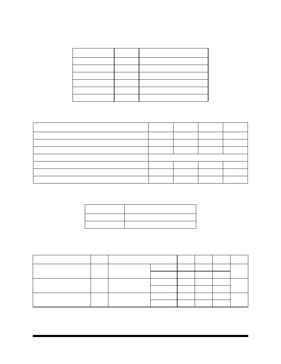
1000560
T
ABLE
1. P
INOUT
D
ESCRIPTION
P
IN
S
YMBOL
D
ESCRIPTION
1, 7, 10, 16
OUT A - D Output Signal
2, 6, 11, 15
-IN A - D
Negative Input Signal
3, 5, 12, 14
+IN A - D
Positive Input Signal
8, 9
NC
Not Connected
4
V+
Positive Voltage
13
V-
Negative Voltage
T
ABLE
2. OP490 A
BSOLUTE
M
AXIMUM
R
ATINGS
P
ARAMETER
S
YMBOL
M
IN
M
AX
U
NIT
Supply Voltage
V
CC
±18
V
Differential Input Voltage
(V-) - 20
(V+) + 20
V
Common-Mode Input Voltage
(V-) - 20
(V+) + 20
V
Output Short-Circuit Duration
Continuous
Thermal Impedance
JC
--
3.35
∞C/W
Storage Temperature Range
T
S
-65
+150
∞C
Operating Temperature Range
T
A
-55
+125
∞C
T
ABLE
3. D
ELTA
L
IMITS
P
ARAMETER
V
ARIATION
I
CC
±10% of specified value in Table 4.
T
ABLE
4. OP490 DC E
LECTRICAL
C
HARACTERISTICS
(VS = ±15
V
, T
A
= -55
TO
125∞C,
UNLESS
OTHERWISE
SPECIFIED
)
P
ARAMETER
S
YMBOL
T
EST
C
ONDITIONS
M
IN
T
YP
M
AX
U
NITS
Input Offset Voltage
V
OS
+25∞C
--
0.2
0.5
mV
-55 to 125∞C
--
0.4
1.0
Input Offset Current
I
OS
V
CM
= 0V
+25∞C
--
0.4
3
nA
-55 to 125∞C
--
1.5
5
Input Bias Current
I
B
V
CM
= 0V
+25∞C
--
4.2
15
nA
-55 to 125∞C
4.4
20
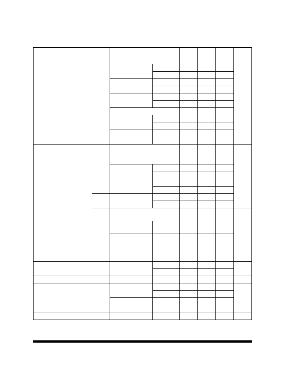
OP490
Memory
3
All data sheets are subject to change without notice
©2001 Maxwell Technologies
All rights reserved.
Low Voltage Micropower Quad Operational Amplifier
12.19.01 Rev2
1000560
Large Signal Voltage Gain
A
VO
V
S
= ±15V, VO = ±10V
V/mV
R
L
= 100 k
+25∞C
700
1200
--
-55 to 125∞C
225
400
--
R
L
= 10 k
+25∞C
350
600
--
-55 to 125∞C
125
240
--
R
L
= 2 k
+25∞C
125
250
--
-55 to 125∞C
50
110
--
V+ = 5V, V- = 0V, 1V<VO<4V
R
L
= 100 k
+25∞C
--
400
--
-55 to 125∞C
--
200
--
R
L
= 10 k
+25∞C
--
180
--
-55 to 125∞C
--
110
--
Input Voltage Range
1
IVR
V+ = 5V, V- = 0V
V
S
= ±15V
0/4
-15/13.5
--
--
--
--
V
Output Voltage Swing
V
O
VS = ±15V
V
RL = 10 k
+25∞C
±13.5
±14.2
--
-55 to 125∞C
±13
±14
--
RL = 2 k
+25∞C
±10.5
±11.5
--
-55 to 125∞C
±10
±11
--
V
OH
V+ = 12V, V- = 0V
RL = 2 k
+25∞C
--
4.2
--
-55 to 125∞C
--
4.1
--
V
OL
V+ = 5V, V- = 0V
RL = 10 k
--
100
--
µV
Common Mode Rejection
CMR
V+ = 5V, V = 0V,
0V < V
CM
< 4
+25∞C
--
110
---
dB
V+ = 5V, V = 0V,
0V < V
CM
< 3.5
-55 to 125∞C
--
108
--
VS = ±15V,
-15V < V
CM
< 13.5V
+25∞C
100
130
--
-55 to 125∞C
95
115
--
Power Supply Rejection Ratio
PSRR
+25∞C
---
1.0
5.6
µV/V
-55 to 125∞C
--
3.2
10
Slew Rate
SR
VS = ±15V
+25∞C
--
12
---
V/ms
Supply Current (All Amplifiers)
I
SY
VS = ±1.5V, No Load
+25∞C
--
40
60
µA
-55 to 125∞C
--
70
100
VS = ±15V, No Load
+25∞C
--
60
80
-55 to 125∞C
--
90
120
Capacitive Load Stability
AV = +1
+25∞C
---
650
---
pF
T
ABLE
4. OP490 DC E
LECTRICAL
C
HARACTERISTICS
(VS = ±15
V
, T
A
= -55
TO
125∞C,
UNLESS
OTHERWISE
SPECIFIED
)
P
ARAMETER
S
YMBOL
T
EST
C
ONDITIONS
M
IN
T
YP
M
AX
U
NITS
OP490
Memory
4
All data sheets are subject to change without notice
©2001 Maxwell Technologies
All rights reserved.
Low Voltage Micropower Quad Operational Amplifier
12.19.01 Rev2
1000560
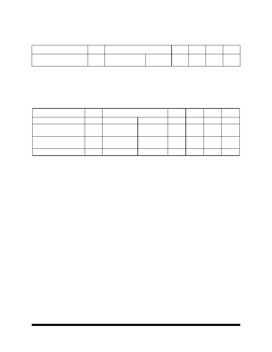
Channel Separation
CS
V
O
= 20Vp-p, f
O
= 10
Hz, VS = ±15V
2
+25∞C
120
150
---
dB
1. Guaranteed by CMR test.
2. Guaranteed but not 100% tested.
T
ABLE
5. OP490 AC E
LECTRICAL
C
HARACTERISTICS
(VS = ±15V, TA = -55
TO
125∞C
UNLESS
OTHERWISE
SPECIFIED
.)
P
ARAMETER
S
YMBOL
T
EST
C
ONDITIONS
M
IN
T
YP
M
AX
U
NIT
Input Noise Voltage
e
n p-p
fO = 0.1 Hz to 10 Hz
+25∞C
---
3
---
µVp-p
Input Resistance Differential
Mode
R
IN
V
S
= ±15V
+25∞C
---
30
---
M
Input Resistance Common
Mode
R
INCM
V
S
= ±15V
+25∞C
---
20
---
G
Gain Bandwidth Product
GBWP A
V
= +1
+25∞C
---
500
---
kHz
T
ABLE
4. OP490 DC E
LECTRICAL
C
HARACTERISTICS
(VS = ±15
V
, T
A
= -55
TO
125∞C,
UNLESS
OTHERWISE
SPECIFIED
)
P
ARAMETER
S
YMBOL
T
EST
C
ONDITIONS
M
IN
T
YP
M
AX
U
NITS
OP490
Memory
5
All data sheets are subject to change without notice
©2001 Maxwell Technologies
All rights reserved.
Low Voltage Micropower Quad Operational Amplifier
12.19.01 Rev2
1000560
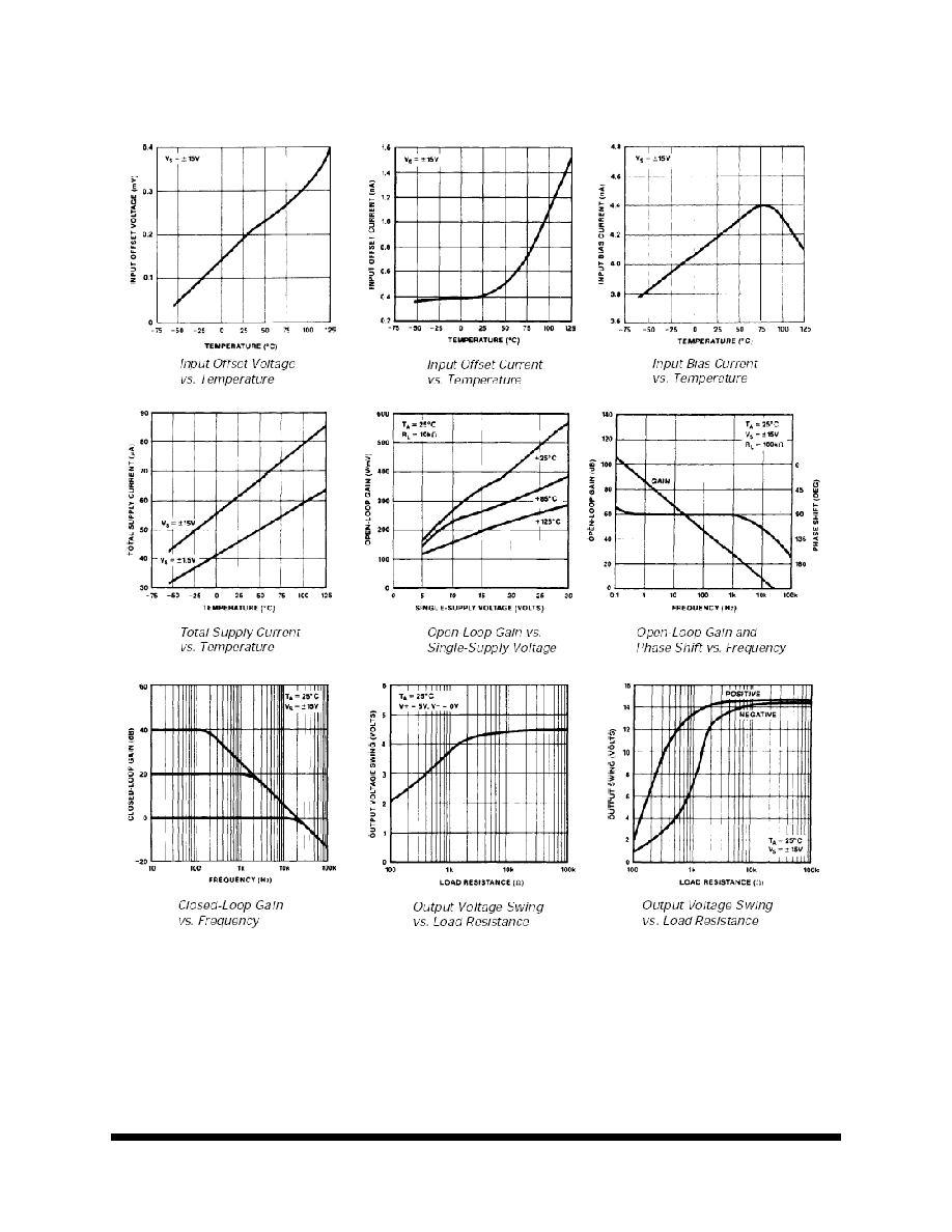
OP490RP T
YPICAL
O
PERATING
C
HARACTERISTICS