 | –≠–ª–µ–∫—Ç—Ä–æ–Ω–Ω—ã–π –∫–æ–º–ø–æ–Ω–µ–Ω—Ç: IFK200 | –°–∫–∞—á–∞—Ç—å:  PDF PDF  ZIP ZIP |

REVISIONS
REV. DESCRIPTION
APPROVED
The information disclosed herein was originated by and is the
property of MAZeT. MAZeT reserves all patent, proprietary, design,
use, sales, manufacturing an reproduction rights thereto. Product
names used in this publication are for identification purposes only
and may be trademark of their respective companies.
1
V1.0
1998-04-06
Approvals
Date
MAZeT GmbH
Compiled:
1998/03/30
Checked:
1998/04/06
Status: valid
MAZeT GmbH Sales
Gˆschwitzer Straþe 32
07745 JENA / GERMANY
Phone: +49 3641 2809-0
Fax: +49 3641 2809-12
E-Mail: sales@MAZeT.de
Url: http://www.MAZeT.de
Released:
1998/04/06
DOC. NO: DB-98-037e
Page 1 of 15
Data Sheet
IFK200
Encoder interface board for PC-AT
Table of contents
1. General Functional Description
2
2. I/O-Addresses And Bus Interface
4
3. Configurations Of The Measuring System
6
3.1 Common control register
6
3.2 Control register of the measuring channels
7
3.3 Timer preset register
8
3.4 Preset registers
9
4. Resources Of The Measuring Systems
9
5. Events Of The Data Logging
9
5.1 Status register
9
5.2 NAS status register
10
6. Interrupt request
10
7. Opto-couplers
11
7.1 Technical data of the opto-coupler inputs
11
8. Presetting
13
9. Connectors allocation
13
10. Constructive Composition
15
REVISIONS
REV. DESCRIPTION
APPROVED
1
V1.0
1998-04-06
The information in this publication is believed to be accurate in all respects at the
time of publication. MAZeT reserves the right to make changes in its products
without notice in order to improve design or performance characteristics.
DOC. NO:
DB-98-037e
Page 2 of 15
DATA SHEET IFK200
1.
GENERAL FUNCTIONAL DESCRIPTION
The interface board "IFK200" contains two channels for data logging. The board is
applicable as 24-Bit counter interface with integrated decoder for digital Z-track signals, as
connection to 2 incremental encoders or as synchronous serial interface (SSI) for 2
absolute encoder.
The board is suitable for applications with length and angle measuring systems and
controlling systems. At incremental mode the encoder with sin/cos-outputs (current
output: 6 µA < Ipp < 16 µA, voltage output: 0.56 V < Upp < 1.5 V) or square pulse
outputs (RS422) can be connected. At SSI mode a connection with to an absolute
encoder RS422-interface is needed.
The following functions are available at incremental mode: edge detection, 24-Bit forward
and backward counter, register, adder, comparator and bus-interface. To get better
resistance against disturbances programmable digital filters are available for the input
signals of the measuring system. A transfer clock of up to 32 pulses is provided at SSI
mode. A serial-to-parallel converter receives encoder data. All functions are
programmable. There is a timer for both modes (incremental and SSI), which is either for
generation of a hardware strobe or for representation of the iteration rate (defined hold
time). The clock frequency of the system equals 25 MHz of cycle time.
There are D-SUB9-connectors for the power supply of plugged encoders. VPLUS is +5V
at incremental mode and +12V at SSI mode. The maximal load per channel is 400
mAmps.
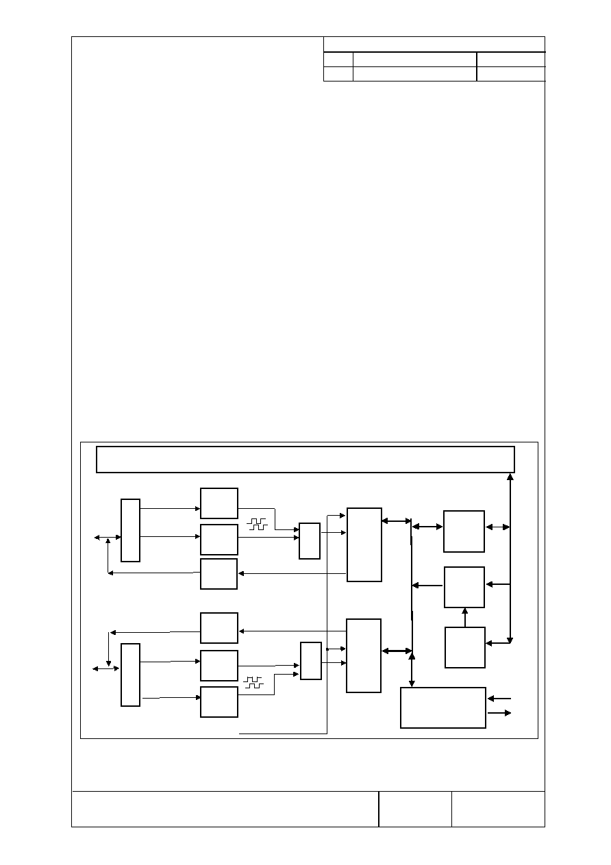
Figure 1 shows the block diagram of the board ,,IFK200".
Figure 1: block diagram ,,IFK200"
A T - B u s
U98221
MAC
Encoder channel 1:
U98221
RS422
RS422
rectangle signals
sin/cos-signals
Encoder channel 2:
2 x
74ACT245
PLD
clk + control signals
4124A
MAC
4124A
RS422
RS422
rectangle signals
sin/cos signals
MX
MX
SSI
SSI
MX
MX
D-Sub 9
D-Sub 9
74ALS688
+
SSI
+
SSI
register +
8 x opto couples
U / I
U / I
D-Sub 25

REVISIONS
REV. DESCRIPTION
APPROVED
1
V1.0
1998-04-06
The information in this publication is believed to be accurate in all respects at the
time of publication. MAZeT reserves the right to make changes in its products
without notice in order to improve design or performance characteristics.
DOC. NO:
DB-98-037e
Page 3 of 15
DATA SHEET IFK200
Generation of square pulses by using of sin/cos-inputs
Figures 2-7 shows the creation of square pulse-signals within the interpolator.
IE1+
IE1-
Figure 2: IE1 = M11, MI21
IE2+
IE2-
Figure 3: IE2 = M12, MI22
Figure 4: Z1 = CHA
Figure 5: Z2 = CHB
RFE+
RFE-
Figure 6: RFE = MI10, MI20
Figure 7: RI = CHC

REVISIONS
REV. DESCRIPTION
APPROVED
1
V1.0
1998-04-06
The information in this publication is believed to be accurate in all respects at the
time of publication. MAZeT reserves the right to make changes in its products
without notice in order to improve design or performance characteristics.
DOC. NO:
DB-98-037e
Page 4 of 15
DATA SHEET IFK200
2.
I/O-ADDRESSES AND BUS INTERFACE
The card module supports exclusive 16-Bit accesses (to even-numbered addresses). The
addresses decode logic is realisable with SA4 ... SA9 and adjustable by using the DIL-
switch S1 (standard value 330/h). The unit needs an address range of 8/h.
The levels of the resources and the board-internal addresses are fixed with writing to offset
address 0 to an internal register. After that the access can be made to the corresponding
resource with offset address 2.
offset addresses
function
0 (write-only)
determination of the level and the board-internal address
2 (read/write)
data access
4
software reset
8
reserved
Table 1a: offset addresses
Table 1b shows the occupancy of the resources and the internal addresses.
D7
D6
D5
D4
D3
D2
D1
D0
reserved
Resource-
level
Resource-
level
address
A4
address
A3
address
A2
address
A1
address
A0
Table 1b: occupancy of the resources and the internal addresses
D6, D5 = 0
level 0:
control register, interrupt-select-RG, opto-coupler
1
level 1:
measuring system channel 1
2
level 2:
measuring system channel 2
3
level 3:
NAS-status register
Tables 2-5 show the addressing of the several resources. The board uses automatic
increment.
Level 0:
A(4:0)
resource
write
read
16
control register
set common control register
1
24
interrupt select register
set interrupt select channel
1, 2
1
28
register opto-coupler
set bit 0 - 3
read bit 4 - 7
1
1
Table 2: address assignment level 0
Level 1, 2: Mode: incremental (SSI = 0)
A(4:0)
resource
write
read
0, 2
strobe register
SW-strobe or write-function
read strobe register ***
1
2
4, 6
preset register (+)
set preset register
read preset register
2
2
8, 10
counter
set counter
read counter ***
1
2
12, 14
reference/offset
register
set reference/offset
register **
read reference
register
2
2

REVISIONS
REV. DESCRIPTION
APPROVED
1
V1.0
1998-04-06
The information in this publication is believed to be accurate in all respects at the
time of publication. MAZeT reserves the right to make changes in its products
without notice in order to improve design or performance characteristics.
DOC. NO:
DB-98-037e
Page 5 of 15
DATA SHEET IFK200
A(4:0)
resource
write
read
16, 18
control register
set control register
read control register
2
2
20
status register
set register for selection of
the resource
read status register with
reset (++)
1
1
24
interrupt mask
set interrupt mask
read interrupt mask
1
1
28
timer incl. register
set timer register
read status register without
reset
1
1
Table 3: address assignment level 1
Level 1, 2: Mode: synchronous serial interface (SSI = 1)
A(4:0)
resource
write
read
0, 2
serial-to-parallel
converter
read serial-to-parallel
converter
2
4
preset register (+)
set preset register
read preset register
1
1
8
frequency divider
read frequency divider
****
1
12, 14
reference/offset
register
set reference/offset
register **
read reference register
2
2
16, 18
control register
set control register
read control register
2
2
20
status register
read status register with
reset (++)
1
24
interrupt mask
set interrupt mask
set interrupt mask
1
1
28
timer incl. register
set timer register
read status register without
reset
1
1
Table 4: address assignment level 2
**
For activated "Add-Offset" bit of the control register the reference/offset registers are loaded with data of the
input registers at a time. For not activated "Add-Offset" bit the reference/offset registers are loaded with the
actual counter value.
***
For activated "Add-Offset" bit the value of the offset register is added on read resource.
****
Function is only for test purposes.
(+)
SSI=0: preset register (24-Bit) for counter, SSI=1: preset register (16-Bit) -> D(15:10) impulse count,
D(9:0) clock frequency
(++) reset status register (except bit 3 - "zero") and reset automatic increment
needed accesses
Two accesses are needed for resources >16-Bit. Thereby the access should be started with the low word.
The high word is assessable with the twice incremented address.
Level 3:
A(4:0)
resource
write
read
28
NAS status register
reset NAS 1, 2
read NAS 1, 2
1
1
Table 5: address assignment level 3