 | –≠–ª–µ–∫—Ç—Ä–æ–Ω–Ω—ã–π –∫–æ–º–ø–æ–Ω–µ–Ω—Ç: MBI5027CP | –°–∫–∞—á–∞—Ç—å:  PDF PDF  ZIP ZIP |

©
Macroblock, Inc. 2003
Floor 6-4, No.18, Pu-Ting Rd., Hsinchu, Taiwan 30077, ROC.
TEL: +886-3-579-0068, FAX: +886-3-579-7534 E-mail:
info@mblock.com.tw
- 1 -
Macroblock
Preliminary Datasheet
MBI5027
16-bit Constant Current LED Sink Driver
with Error Detection
Features
∑
Error Detection mode to detect LED open-circuit errors
∑
16 constant-current output channels
∑
Constant output current invariant to load voltage change
∑
Excellent output current accuracy:
between channels:
±
3% (max.), and
between ICs:
±
6% (max.)
∑
Output current adjusted through an external resistor
∑
Constant output current range: 5-90 mA
∑
Fast response of output current,
OE
(min.): 200 ns
∑
25MHz clock frequency
∑
Schmitt trigger input
∑
5V supply voltage
Current Accuracy
Between Channels
Between ICs
Conditions
<
±
3%
<
±
6%
I
OUT
= 10 mA ~ 60 mA
MBI5016CP
MBI5016CF
MBI5016CNS
MBI5027CNS
MBI5027CP
MBI5027CF

MBI5027
16-bit Constant Current LED Sink Driver with Error Detection
April 2003, V0.8-4
- 2 -
Product Description
MBI5027 succeeds MBI5026 and is designed for LED displays with open-circuit Error Detection
extension. MBI5027 exploits PrecisionDrive
TM
technology to enhance its output characteristics.
MBI5027 contains a serial buffer and data latches, which convert serial input data into parallel
output format. At MBI5027 output stage, sixteen regulated current ports are designed to provide
uniform and constant current sinks for driving LEDs within a wide range of Vf variations.
While MBI5027 is used in their system design for LED display applications, e.g. LED panels, it
provides users with great flexibility and device performance. Users may adjust the output
current from 5 mA to 90 mA through an external resistor, R
ext
, which gives users flexibility in
controlling the light intensity of LEDs. MBI5027 guarantees to endure maximum 17V at the
output port. The high clock frequency, 25 MHz, also satisfies the system requirements of high
volume data transmission.
MBI5027 exploits the idea of Share-I-O
TM
technology to extend its performance
in addition,
MBI5027 is backward compatible with MBI5026 in both electrical characteristics and package
aspect. With Share-I-O
TM
technology, users can, without changing the printed circuit board
originally for MBI5026, let MBI5027 enter a special function mode, an Error Detection mode,
just by setting a sequence of signals on LE(ED1),
OE
(ED2) and CLK input pins. In the Error
Detection mode, MBI5027 detects the status of individual LED connected to MBI5027. The
status will be saved in a built-in register. Then, a system controller may read, through SDO pin,
the error status from the register to know whether LEDs are properly lit or not. By setting
another sequence of signals on LE(ED1),
OE
(ED2) and CLK input pins, MBI5027 may resume
to a Normal mode and perform as MBI5026. In Application Information, users can get
detailed ideas about how MBI5027 works in the Error Detection mode.
A Share-I-O
TM
technique is specifically applied to MBI5027. By means of the Share-I-O
TM
technique, an additionally effective function, Error Detection, can be added to LED drivers,
however, without any extra pins. Thus, MBI5027 could be a drop-in replacement of MBI5026.
The printed circuit board originally designed for MBI5026 may be also applicable for MBI5027.
For MBI5027, the pin 4, LE(ED1), and the pin 21, OE (ED2), can be acted as different functions
as follows:
Pin
Device Name
MBI5027
Function Description of Pin 4
LE + Error Detection (ED1)
Function Description of Pin 21
OE + Error Detection (ED2)

MBI5027
16-bit Constant Current LED Sink Driver with Error Detection
April 2003, V0.8-4
- 3 -
GND
SDI
CLK
LE(ED1)
OUT7
OE(ED2)
SDO
R-EXT
VDD
1
2
3
4
5
6
7
8
9
10
11
12
13
14
15
16
17
18
19
20
21
22
23
24
OUT8
OUT6
OUT5
OUT4
OUT3
OUT2
OUT1
OUT0
OUT9
OUT10
OUT11
OUT12
OUT13
OUT14
OUT15
Block Diagram
Terminal Description
Pin No.
Pin Name
Function
1
GND
Ground terminal for control logic and
current sink
2
SDI
Serial-data input to the Shift Register
3
CLK
Clock input terminal for data shift on
rising edge
4
LE(ED1)
Data strobe input terminal
Serial data is transferred to the
respective latch when LE(ED1) is high.
The data is latched when LE(ED1)
goes low.
Also, a control signal input for Error
Detection mode (See Timing Diagram)
5~20
OUT0 ~ OUT15 Constant current output terminals
21
OE (ED2)
Output enable terminal
When (active) low, the output drivers
are enabled; when high, all output
drivers are turned OFF (blanked).
Also, a control signal input for Error
Detection mode (See Timing Diagram)
22
SDO
Serial-data output to the following SDI
of next driver IC
23
R-EXT
Input terminal used to connect an
external resistor for setting up all output
current
24
VDD
5V supply voltage terminal
Pin Configuration
16-bit Shift Register
16-bit Output Latch
I
O
Regulator
Output Driver & Error Detector
Control Logic
R-EXT
SDI
CLK
SDO
16
16
GND
VDD
LE(ED1)
16
OUT0
1
OUT
OUT14
OUT15
)
2
ED
(
OE

MBI5027
16-bit Constant Current LED Sink Driver with Error Detection
April 2003, V0.8-4
- 4 -
Equivalent Circuits of Inputs and Outputs
terminal
LE(ED1) terminal
)
2
ED
(
OE
VDD
VDD
VDD
VDD
CLK, SDI terminal
SDO terminal
IN
IN
IN
OUT
MBI5027
16-bit Constant Current LED Sink Driver with Error Detection
April 2003, V0.8-4
- 5 -
Timing Diagram
Normal Mode
Truth Table (In Normal Mode)
CLK
LE
OE
SDI
OUT0 ...
7
OUT ... OUT15
SDO
H
L
D
n
n
D
...
.
7
-
n
D
...
.
15
-
n
D
D
n-15
L
L
D
n+1
No Change
D
n-14
H
L
D
n+2
2
+
n
D
...
.
5
-
n
D
...
.
13
-
n
D
D
n-13
X
L
D
n+3
2
+
n
D
...
.
5
-
n
D
...
.
13
-
n
D
D
n-13
X
H
D
n+3
Off
D
n-13
CLK
SDI
N = 0
1 2
3 4
5 6
7 8
9 10
11 12
13 14 15
LE(ED2)
OFF
ON
OFF
ON
OFF
ON
OFF
ON
OFF
ON
SDO
: don
'
t care
)
2
ED
(
OE
OUT0
1
OUT
OUT2
OUT3
OUT15

MBI5027
16-bit Constant Current LED Sink Driver with Error Detection
April 2003, V0.8-4
- 6 -
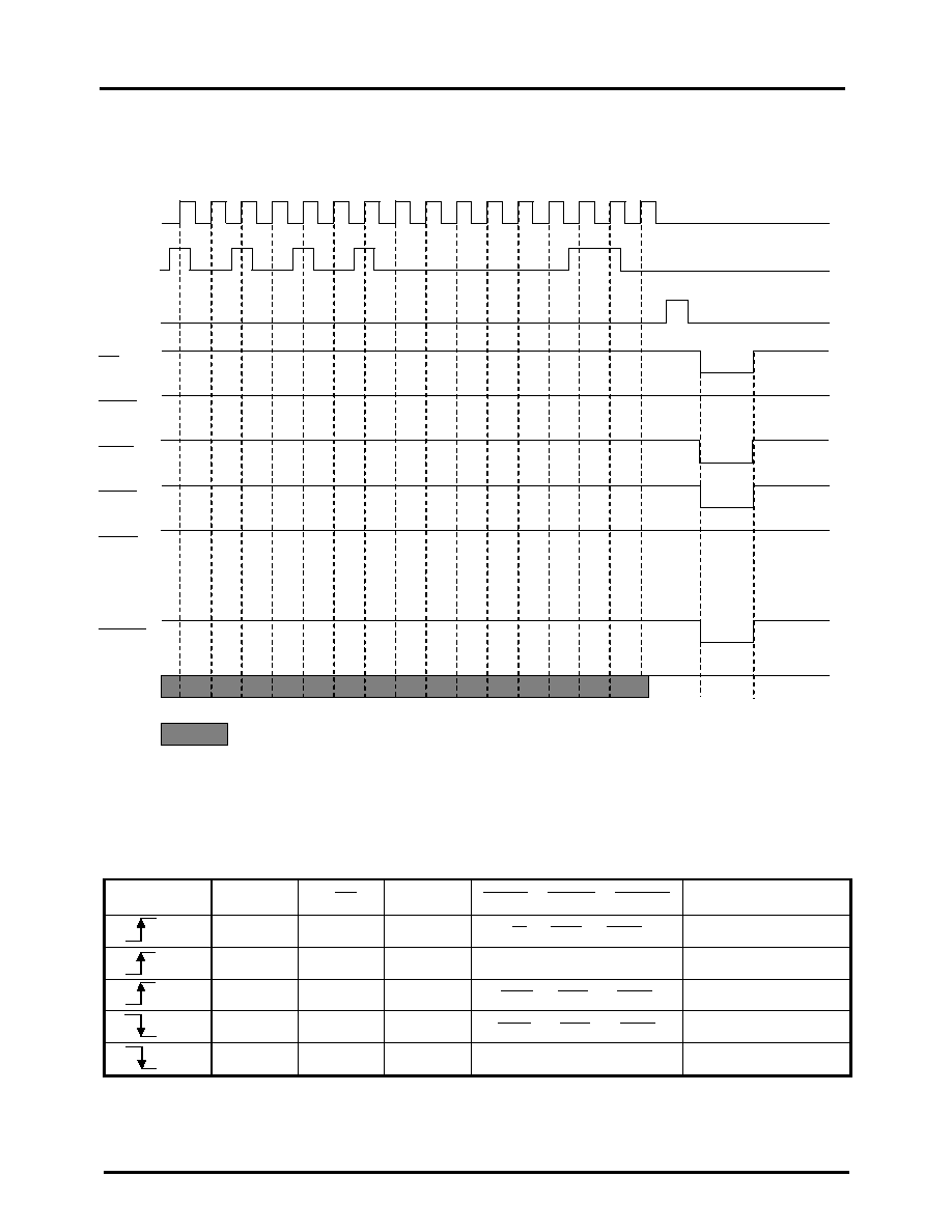
Entering Error Detection Mode
The signal sequence makes MBI5027 enter an Error Detection mode.
Reading Error Status Code
A system controller can read Error Status codes through SDO pin.
Resuming to Normal Mode
The signal sequence makes MBI5027 resume to the Normal mode.
Note:
If users want to know the whole process, that is how to enter the Error Detection mode, read Error
Status codes and resume to the Normal mode, please refer to the contents in Application Information.
: don
'
t care
about 2
s
Bit15 Bit14
Error Status Code
Bit13 Bit12 Bit11
CLK
SDO
(ED2)
OE
LE(ED1)
CLK
1 2
3 4 5
1
0
1
1
1
0
0
0
1
0
)
2
ED
(
OE
CLK
LE(ED1)
1 2
3 4 5
1
0
1
1
1
0
0
0
0
0
Voltage
"
Low
"
)
2
ED
(
OE

MBI5027
16-bit Constant Current LED Sink Driver with Error Detection
April 2003, V0.8-4
- 7 -
Maximum Ratings
Characteristic
Symbol
Rating
Unit
Supply Voltage
V
DD
0~7.0
V
Input Voltage
V
IN
-0.4~V
DD
+ 0.4
V
Output Current
I
OUT
+90
mA
Output Voltage
V
DS
-0.5~+20.0
V
Clock Frequency
F
CLK
25
MHz
GND Terminal Current
I
GND
1440
mA
CNS
≠
type
1.52
CF
≠
type
1.30
Power Dissipation
(On PCB, Ta=25
∞
C)
CP
≠
type
P
D
1.11
W
CNS
≠
type
82
CF
≠
type
96
Thermal Resistance
(On PCB, Ta=25
∞
C)
CP
≠
type
R
th(j-a)
112
∞
C/W
Operating Temperature
T
opr
-40~+85
∞
C
Storage Temperature
T
stg
-55~+150
∞
C

MBI5027
16-bit Constant Current LED Sink Driver with Error Detection
April 2003, V0.8-4
- 8 -
Recommended Operating Conditions
Characteristic
Symbol
Condition
Min.
Typ.
Max.
Unit
Supply Voltage
V
DD
-
4.5
5.0
5.5
V
Output Voltage
V
DS
OUT0 ~ OUT15
-
-
17.0
V
I
OUT
DC Test Circuit
5
-
60
mA
I
OH
SDO
-
-
-1.0
mA
Output Current
I
OL
SDO
-
-
1.0
mA
V
IH
CLK, OE (ED2),
LE(ED1) and SDI
0.8V
DD
-
V
DD
+0.3
V
Input Voltage
V
IL
CLK, OE (ED2),
LE(ED1) and SDI
-0.3
-
0.3V
DD
V
LE(ED1) Pulse Width
t
w(L)
40
-
-
ns
CLK Pulse Width
t
w(CLK)
20
-
-
ns
OE (ED2) Pulse Width
t
w(OE)
200
-
-
ns
Setup Time for SDI
t
su(D)
5
-
-
ns
Hold Time for SDI
t
h(D)
10
-
-
ns
Setup Time for LE(ED1)
t
su(L)
15
-
-
ns
Hold Time for LE(ED1)
t
h(L)
Normal Mode
V
DD
=4.5~5.5V
15
-
-
ns
OE (ED2) Pulse Width
t
w(ED2)
2
-
-
us
CLK Pulse Width
t
w(CLK)
20
-
-
ns
Setup Time for LE(ED1)
t
su(ED1)
5
-
-
ns
Hold Time for LE(ED1)
t
h(ED1)
10
-
-
ns
Setup Time for OE (ED2)
t
su(ED2)
5
-
-
ns
Hold Time for OE (ED2)
t
h(ED2)
Error Detection Mode
V
DD
=4.5~5.5V
10
-
-
ns
Clock Frequency
F
CLK
Cascade Operation
-
-
25.0
MHz
Ta=85
∞
C (CNS type)
-
-
0.79
Ta=85
∞
C (CF type)
-
-
0.67
Power Dissipation
P
D
Ta=85
∞
C (CP type)
-
-
0.57
W

MBI5027
16-bit Constant Current LED Sink Driver with Error Detection
April 2003, V0.8-4
- 9 -
Electrical Characteristics
Characteristic
Symbol
Condition
Min.
Typ.
Max.
Unit
"
H
"
level
V
IH
Ta = -40~85
∫
C
0.8V
DD
-
V
DD
V
Input
Voltage
"
L
"
level
V
IL
Ta = -40~85
∫
C
GND
-
0.3V
DD
V
Output Leakage Current
I
OH
V
OH
=17.0V
-
-
0.5
A
V
OL
I
OL
=+1.0mA
-
-
0.4
V
Output
Voltage
SDO
V
OH
I
OH
=-1.0mA
4.6
-
-
V
Output Current 1
I
OUT1
V
DS
=0.6V
R
ext
=720
-
25.0
-
mA
Current Skew
dI
OUT1
I
OL
=25mA
V
DS
=0.6V
R
ext
=720
-
±
1
±
3
%
Output Current 2
I
OUT2
V
DS
=0.8V
R
ext
=360
-
50.0
-
mA
Current Skew
dI
OUT2
I
OL
=50mA
V
DS
=0.8V
R
ext
=360
-
±
1
±
3
%
Output Current vs.
Output Voltage Regulation
%/dV
DS
V
DS
within 1.0V and 3.0V
-
±
0.1
-
% / V
Output Current vs.
Supply Voltage Regulation
%/dV
DD
V
DD
within 4.5V and 5.5V
-
±
1
-
% / V
Pull-up Resistor
R
IN
(up)
OE (ED2)
250
500
800
K
Pull-down Resistor
R
IN
(down)
LE(ED1)
250
500
800
K
V
DS, Th1
When all output ports sink 20mA
simultaneously
1.0
-
-
V
V
DS, Th2
When a single output port sinks
20mA
0.8
-
-
V
V
DS, Th3
When all output ports sink 50mA
simultaneously
1.2
-
-
V
Open Circuit Error***
Discrimination Voltage
V
DS, Th4
When a single output port sinks
50mA
1.0
-
-
V
I
DD
(off) 1 R
ext
=Open, OUT0 ~ OUT15 =Off
-
9
-
I
DD
(off) 2 R
ext
=720
,
OUT0 ~ OUT15 =Off
-
11
-
"
OFF
"
I
DD
(off) 3 R
ext
=360
,
OUT0 ~ OUT15 =Off
-
14
-
I
DD
(on) 1 R
ext
=720
, OUT0 ~ OUT15 =On
-
11
-
Supply
Current
"
ON
"
I
DD
(on) 2 R
ext
=360
, OUT0 ~ OUT15 =On
-
14
-
mA
***
To effectively detect the error occurring at the output port, MBI5027 has a built-in current detection
circuit. The current detection circuit will detect the effective current I
OUT, effective
, and compare the effective
current I
OUT, effective
, to the target current I
OUT
, target
, defined by
R
ext
. If I
OUT, effective
, is much less than the
target current I
OUT
, target
, an error flag will be asserted in the built-in Shift Register. The minimum voltage
requirement for such current detection is V
DS, Th1
, V
DS, Th2
, V
DS, Th3
and V
DS, Th4
.
MBI5027
16-bit Constant Current LED Sink Driver with Error Detection
April 2003, V0.8-4
- 10 -
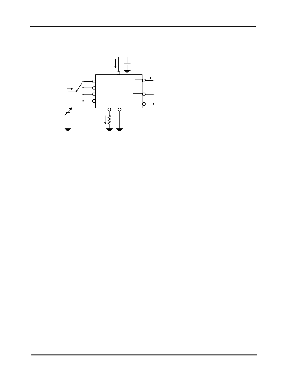
Test Circuit for Electrical Characteristics
(ED2)
OE
CLK
LE(ED1)
SDI
DD
V
EXT
-
R
GND
SDO
OUT0
OUT15
.
.
.
.
DD
I
OUT
I
ref
I
IL
IH,
V
V
IL
IH,
I
I

MBI5027
16-bit Constant Current LED Sink Driver with Error Detection
April 2003, V0.8-4
- 11 -
Switching Characteristics
Characteristic
Symbol Condition
Min.
Typ. Max.
Unit
CLK - OUTn
t
pLH1
-
50
100
ns
LE(ED1) - OUTn
t
pLH2
-
50
100
ns
OE (ED2) - OUTn
t
pLH3
-
20
100
ns
Propagation Delay Time
(
"
L
"
to
"
H
"
)
CLK - SDO
t
pLH
15
20
-
ns
CLK - OUTn
t
pHL1
-
100
150
ns
LE(ED1) - OUTn
t
pHL2
-
100
150
ns
OE (ED2) - OUTn
t
pHL3
-
50
150
ns
Propagation Delay Time
(
"
H
"
to
"
L
"
)
CLK - SDO
t
pHL
15
20
-
ns
CLK
t
w(CLK)
20
-
-
ns
LE(ED1)
t
w(L)
20
-
-
ns
Pulse Width
OE (ED2)
t
w(OE)
200
-
-
ns
Hold Time for LE(ED1)
t
h(L)
5
-
-
ns
Setup Time for LE(ED1)
t
su(L)
V
DD
=5.0 V
V
DS
=0.8 V
V
IH
=V
DD
V
IL
=GND
R
ext
=300
V
L
=4.0 V
R
L
=52
C
L
=10 pF
5
-
-
ns
Maximum CLK Rise Time
t
r
**
-
-
500
ns
Maximum CLK Fall Time
t
f
**
-
-
500
ns
Output Rise Time of Iout
t
or
-
70
200
ns
Output Fall Time of Iout
t
of
-
40
120
ns
**If the devices are connected in cascade and t
r
or t
f
is large, it may be critical to achieve the timing required for
data transfer between two cascaded devices.
Test Circuit for Switching Characteristics
(ED2)
OE
CLK
LE(ED1)
DD
V
EXT
-
R
GND
SDO
OUT0
OUT15
.
.
.
Generator
Function
DD
I
OUT
I
ref
I
L
R
L
C
L
C
L
V
IL
IH,
V
V
5V
V
IH
=
0V
V
IL
=
waveform
input
Logic
ns
10
t
t
f
r
=
=
SDI

MBI5027
16-bit Constant Current LED Sink Driver with Error Detection
April 2003, V0.8-4
- 12 -
Timing Waveform
Normal Mode
t
su(D)
t
h(D)
t
pLH
,
t
pHL
50%
50%
50%
50%
50%
t
W(L)
50%
50%
50%
t
h(L)
t
pLH2
,
t
pHL2
LE(ED1)
SDI
CLK
SDO
LOW = OUTPUTS ENABLED
HIGH = OUTPUT OFF
LOW = OUTPUT ON
t
pLH1
,
t
pHL1
50%
t
su(L)
t
W(CLK)
)
2
ED
(
OE
OUTn
50%
50%
t
pHL3
50%
50%
t
pLH3
t
W(OE)
90%
10%
10%
90%
t
of
t
or
)
2
ED
(
OE
OUTn

MBI5027
16-bit Constant Current LED Sink Driver with Error Detection
April 2003, V0.8-4
- 13 -
Entering Error Detection Mode
Reading Error Status Code
t
su(ED2)
t
h(ED2)
50%
50%
50%
50%
CLK
50%
50%
50%
50%
50%
t
su(ED1)
t
h(ED1)
LE(ED1)
t
W(CLK)
2 CLK
)
2
ED
(
OE
50%
50%
CLK
50%
50%
t
w(ED2)
)
2
ED
(
OE

MBI5027
16-bit Constant Current LED Sink Driver with Error Detection
April 2003, V0.8-4
- 14 -
Application Information
Constant Current
To design LED displays, MBI5027 provides nearly no variations in current from channel to
channel and from IC to IC. This can be achieved by:
1) The maximum current variation between channels is less than
±
3% and that between ICs is
less than
±
6%.
2) In addition, the current characteristic of output stage is flat and users can refer to the figure
as shown below. The output current can be kept constant regardless of the variations of LED
forward voltages (Vf). This performs as a complete function of the load regulation.
0.00
10.00
20.00
30.00
40.00
50.00
60.00
70.00
80.00
90.00
100.00
0
0.1
0.2
0.3
0.4
0.5
0.6
0.7
0.8
0.9
1
1.1
1.2
1.3
1.4
1.5
2
2.5
V
DS
(V)
I
o
u
t
(
m
A
)

MBI5027
16-bit Constant Current LED Sink Driver with Error Detection
April 2003, V0.8-4
- 15 -
0
10
20
30
40
50
60
70
80
90
100
0
500
1000
1500
2000
2500
3000
3500
4000
Adjusting Output Current
The output current of each channel (I
OUT
) is set by an external resistor, R
ext
. The relationship
between I
out
and R
ext
is shown in the following figure.
Also, the output current in milliamps can be calculated from the equation:
I
OUT
is (625/ R
ext
) x 28.8, approximately,
where R
ext
, in
, is the resistance of the external resistor connected to R-EXT terminal.
The magnitude of current is around 50mA at 360
and 25mA at 720
.
Resistance of the external resistor, R
ext
, in
V
DS
= 1.0V
I
OUT
(mA)

MBI5027
16-bit Constant Current LED Sink Driver with Error Detection
April 2003, V0.8-4
- 16 -
Entering Error Detection Mode
Each time the system controller sends the sequence patterns shown above, MBI5027 can enter
the Error Detection mode. During this phase, the system controller can still send data through
SDI pin.
The state of
OE
(ED2) and LE(ED1) is sampled by the rising edge of each CLK. We use
"
0
"
and
"
1
"
to represent the state of
"
Voltage Low
"
and
"
Voltage High
"
respectively. The states of
the successive five
OE
(ED2) and LE(ED1) are (1, 0), (0, 0), (1, 0), (1, 1) and (1, 0).
Reading Error Status Code
Once entering the Error Detection mode, the Error Detection takes place by changing the state
of
OE
(ED2) from
"
Voltage High
"
to
"
Voltage Low
"
.
T
he built-in current detection circuit will
detect the effective current I
OUT, effective
of each output channel, and compare it to the target
current I
OUT, target
, defined by R
ext
.
If the I
OUT, effective
, is much less than the target current I
OUT, target
,
an error status code will be represented as
"
0
"
state.
During the period of detecting errors, data
cannot be sent into MBI5027 through SDI pin. The
"
Voltage Low
"
state of
OE
(ED2) requires at
least three
"
0
"
of which the last
"
0
"
should be at least 2
s after the falling edge of
OE
(ED2).
The occurrence of the last
"
0
"
results in the event that MBI5027 saves the error status in the
built-in register. The mentioned state of each
"
0
"
is sampled by the rising edge of each CLK.
Before the error status saved in the built-in register is read, the state of
OE
(ED2) should be
pulled up from
"
Voltage Low
"
to
"
Voltage High
"
. Then, by sending CLK, MBI5027 shifts out,
through SDO pin, the error status bit by bit.
LE(ED1)
CLK
1 2
3 4 5
1
0
1
1
1
0
0
0
1
0
)
2
ED
(
OE
about 2
s
Bit15 Bit14
Error Status Code
Bit13 Bit12 Bit11
SDO
CLK
)
2
ED
(
OE
1 0
0
0
1
1
1
1

MBI5027
16-bit Constant Current LED Sink Driver with Error Detection
April 2003, V0.8-4
- 17 -
Resuming to Normal Mode
Each time the system controller sends the sequence patterns shown above, MBI5027 can
resume to the Normal mode. During this phase, the system controller can still send data
through SDI pin.
The state of
OE
(ED2) and LE(ED1) is sampled by the rising edge of each CLK. We use
"
0
"
and
"
1
"
to represent the state of
"
Voltage Low
"
and
"
Voltage High
"
respectively. The states of
the successive five
OE
(ED2) and LE(ED1) are (1, 0), (0, 0), (1, 0), (1, 0) and (1, 0).
CLK
LE(ED1)
1 2
3 4 5
1
0
1
1
1
0
0
0
0
0
Voltage
"
Low
"
)
2
ED
(
OE

MBI5027
16-bit Constant Current LED Sink Driver with Error Detection
April 2003, V0.8-4
- 18 -
Timing Chart for Error Detection Mode (An Example)
N x 16 -1
Serial Data (Note 1)
14
15
1
2
3
4
5
1
2
3
4
5
Resuming to the
Normal Mode
Entering the Error
Detection Mode
Sending the Normal Image Data (or Test Data)
Serial Data k, k = 0
...
(N x 16
≠
1)
Reading Back the Error Status Code
30
1
2
Detecting the Error Status
SDI, 0
N x 16
N x 16 CLK Pulses (Note 3)
N x 16 CLK Pulses (Note 1)
SDI, 0
N-1
SDI, 0
3 CLK Pulses Required (Note 2)
MBI5027, 0
N x MBI5027 are connected in cascade, ie, SDO, k --> SDI, k+1.
And, all MBI5027 ICs are connected to the same CLK, LE(ED1) and OE (ED2)
signals.
SDI, 0
SDO, 2
SDO, N-1
N-1
MBI5027, 1
MBI5027, 2
MBI5027, N-1
Note 2:
T1 = 2 CLK pluses is required to start the error detection.
T2 = 2
s is required to obtain the stable error status result.
T3 = the third CLK pulses is required before OE (ED2) goes
voltage high. The rising edge of CLK writes the error status code
back to the MBI5027 built-in shift register.
Note 3:
The first rising edge of CLK after the rising edge of OE (ED2) starts shifting the Image
Data with LED Error. An LED error will be represented by a
"
0
"
, to over write the
original image data
"
1
"
. Image Data k, k = 0
...
(N x 16
≠
1), = all
"
1
"
is suggested.
N x 16 CLK pulses shift all N x 16 error results (Error Status Code) via Node SDO, N
0
Note 1: N x 16 CLK pulses before the
next LE shift the valid image data. N x
16
"
1
"
s are suggested.
2
1
0
LED j, j = 0
...
(N x16
≠
1)
Don
'
t Care
Could Be
"
Don
'
t Care
"
SDO, 1
SDI, 1
SDO, 0
N-1
D
B
A
SDO, 1
SDO, 0
N-1
T2 = 2
µ
s
T1 = 2 CLK
T3 (Note 2)
C
t
h(L)
LE(ED1)
LE(ED1)
CLK
CLK
LE(ED1)
31
SDO, N-1
N-1
N x 16 -2
MBI5027, N-2
OE
(ED2)
OE
(ED2)
OE
(ED2)

MBI5027
16-bit Constant Current LED Sink Driver with Error Detection
April 2003, V0.8-4
- 19 -
Package Power Dissipation (P
D
)
The maximum allowable package power dissipation is determined as P
D
(max) = (Tj
≠
Ta) /
R
th(j-a)
. When 16 output channels are turned on simultaneously, the actual package power
dissipation is P
D
(act) = (I
DD
x V
DD
) + (I
OUT
x Duty x V
DS
x 16). Therefore, to keep P
D
(act)
P
D
(max), the allowable maximum output current as a function of duty cycle is:
I
OUT
= { [ (Tj
≠
Ta) / R
th(j-a)
]
≠
(I
DD
x V
DD
) } / V
DS
/ Duty / 16,
where Tj = 150
∞
C.
(A) I
out
= 90mA, V
DS
= 1.0V, 16 output channels active
For CNS type package, the thermal resistance is R
th(j-a)
= 82 (
∞
C/W)
0
10
20
30
40
50
60
70
80
90
100
5
%
1
0
%
1
5
%
2
0
%
2
5
%
3
0
%
3
5
%
4
0
%
4
5
%
5
0
%
5
5
%
6
0
%
6
5
%
7
0
%
7
5
%
8
0
%
8
5
%
9
0
%
9
5
%
1
0
0
%
Duty Cycle
I
o
u
t
(
m
A
)
Ta = 25
∞
C
Ta = 55
∞
C
Ta = 85
∞
C
Iout vs. Duty Cycle at Rth = 82 (
∞
C/W)
For CF type package, the thermal resistance is Rth(j-a) = 96 (
∞
C/W)
0
10
20
30
40
50
60
70
80
90
100
5
%
1
0
%
1
5
%
2
0
%
2
5
%
3
0
%
3
5
%
4
0
%
4
5
%
5
0
%
5
5
%
6
0
%
6
5
%
7
0
%
7
5
%
8
0
%
8
5
%
9
0
%
9
5
%
1
0
0
%
Duty Cycle
I
o
u
t
(
m
A
)
Ta = 25
Ta = 55
Ta = 85
Iout vs. Duty Cycle at Rth = 96 (
∞
C/W)

MBI5027
16-bit Constant Current LED Sink Driver with Error Detection
April 2003, V0.8-4
- 20 -
For CP type package, the thermal resistance is R
th(j-a)
= 112 (
∞
C/W)
Iout vs. Duty Cycle at Rth = 112 (
∞
C/W)
0
10
20
30
40
50
60
70
80
90
100
5
%
1
0
%
1
5
%
2
0
%
2
5
%
3
0
%
3
5
%
4
0
%
4
5
%
5
0
%
5
5
%
6
0
%
6
5
%
7
0
%
7
5
%
8
0
%
8
5
%
9
0
%
9
5
%
1
0
0
%
Duty Cycle
I
o
u
t
(
m
A
)
Ta = 25
∞
C
Ta = 55
∞
C
Ta = 85
∞
C
(B) I
out
= 60mA, V
DS
= 0.8V, 16 output channels active
For CNS type package, the thermal resistance is R
th(j-a)
= 82 (
∞
C/W)
Iout vs. Duty Cycle at Rth = 82 (
∞
C/W)
0
10
20
30
40
50
60
70
5
%
1
0
%
1
5
%
2
0
%
2
5
%
3
0
%
3
5
%
4
0
%
4
5
%
5
0
%
5
5
%
6
0
%
6
5
%
7
0
%
7
5
%
8
0
%
8
5
%
9
0
%
9
5
%
1
0
0
%
Duty Cycle
I
o
u
t
(
m
A
)
Ta = 25
∞
C
Ta = 55
∞
C
Ta = 85
∞
C

MBI5027
16-bit Constant Current LED Sink Driver with Error Detection
April 2003, V0.8-4
- 21 -
For CF type package, the thermal resistance is R
th(j-a)
= 96 (
∞
C/W)
Iout vs. Duty Cycle at Rth = 96 (
∞
C/W)
0
10
20
30
40
50
60
70
5
%
1
0
%
1
5
%
2
0
%
2
5
%
3
0
%
3
5
%
4
0
%
4
5
%
5
0
%
5
5
%
6
0
%
6
5
%
7
0
%
7
5
%
8
0
%
8
5
%
9
0
%
9
5
%
1
0
0
%
Duty Cycle
I
o
u
t
(
m
A
)
Ta = 25
∞
C
Ta = 55
∞
C
Ta = 85
∞
C
For CP type package, the thermal resistance is R
th(j-a)
= 112 (
∞
C/W)
Iout vs. Duty Cycle at Rth = 112 (
∞
C/W)
0
10
20
30
40
50
60
70
5
%
1
0
%
1
5
%
2
0
%
2
5
%
3
0
%
3
5
%
4
0
%
4
5
%
5
0
%
5
5
%
6
0
%
6
5
%
7
0
%
7
5
%
8
0
%
8
5
%
9
0
%
9
5
%
1
0
0
%
Duty Cycle
I
o
u
t
(
m
A
)
Ta = 25
∞
C
Ta = 55
∞
C
Ta = 85
∞
C

MBI5027
16-bit Constant Current LED Sink Driver with Error Detection
April 2003, V0.8-4
- 22 -
The maximum power dissipation, P
D
(max)
=
(Tj-Ta) / R
th(j-a)
, decreases as the ambient
temperature increases.
Max. Power Dissipation at Various Ambient Temperature
0
0.2
0.4
0.6
0.8
1
1.2
1.4
1.6
-40
-30
-20
-10
0
10
20
30
40
50
60
70
80
90
Ambient Temperature
P
o
w
e
r
D
i
s
s
i
p
a
t
i
o
n
CNS Type: Rth = 82
CF Type: Rth = 96
CP Type: Rth = 112
Load Supply Voltage (V
LED
)
MBI5027 are designed to operate with V
DS
ranging from 0.4V to 1.0V considering the package
power dissipating limits. V
DS
may be higher enough to make P
D(act)
> P
D(max)
when V
LED
= 5V
and V
DS
= V
LED
≠
Vf, in which V
LED
is the load supply voltage. In this case, it is recommended to
use the lowest possible supply voltage or to set an external voltage reducer, V
DROP
.
A voltage reducer lets V
DS
= (V
LED
≠
Vf)
≠
V
DROP
.
Resistors or Zener diode can be used in the applications as the following figures.
V
LED
V
DROP
Vf
V
DS
MBI5027
V
LED
V
DROP
Vf
V
DS
MBI5027

MBI5027
16-bit Constant Current LED Sink Driver with Error Detection
April 2003, V0.8-4
- 23 -
Package Outlines
MBI5027CNS Outline Drawing
MBI5027CF Outline Drawing
SDIP-24-P-300-1.78
Units: mm
Weight: 1.11g (typ)
SOP-24-P-300-1.00
Units: mm
Weight: 0.28g (typ)

MBI5027
16-bit Constant Current LED Sink Driver with Error Detection
April 2003, V0.8-4
- 24 -
MBI5027CP Outline Drawing
SSOP24-P-150-0.64
Units: mm
Weight: 0.11g (typ)