©
Macroblock, Inc. 2003
Floor 6-4, No.18, Pu-Ting Rd., Hsinchu, Taiwan 30077, ROC.
TEL: +886-3-579-0068, FAX: +886-3-579-7534 E-mail:
info@mblock.com.tw
- 1 -
Macroblock
Advance Information
MBI5168
8-bit Constant Current LED Sink Driver
Features
l
8 constant-current output channels
l
Constant output current invariant to load voltage change
l
Excellent output current accuracy:
between channels: <
±
4% (max.), and
between ICs: <
±
6% (max.)
l
Output current adjusted through an external resistor
l
Constant output current range: 5 -120 mA
l
Fast response of output current, /OE (min.): 400 ns
l
25MHz clock frequency
l
Schmitt trigger input
l
5V supply voltage
Product Description
MBI5168 is designed for LED displays. As an enhancement of its predecessor, MBI5001,
MBI5168 exploits PrecisionDrive
TM
technology to enhance its output characteristics. MBI5168
contains a serial buffer and data latches which convert serial input data into parallel output
format. At MBI5168 output stage, eight regulated current ports are designed to provide uniform
and constant current sinks for driving LEDs within a large range of Vf variations.
MBI5168 provides users with great flexibility and device performance while using MBI5168 in
their system design for LED display applications, e.g. LED panels. Users may adjust the output
current from 5 mA to 120 mA through an external resistor, R
ext
, which gives users flexibility in
controlling the light intensity of LEDs. MBI5168 guarantees to endure maximum 17V at the
output port. The high clock frequency, 25 MHz, also satisfies the system requirements of high
volume data transmission.
Current Accuracy
Between Channels
Between ICs
Conditions
<
±
4%
<
±
6%
I
OUT
= 10 mA to 60 mA, V
DS
= 0.6V
<
±
6%
<
±
12%
I
OUT
= 60 mA to100 mA, V
DS
= 0.8V
M B I5 0 0 1 C N
MBI5001CN
MBI5168CN
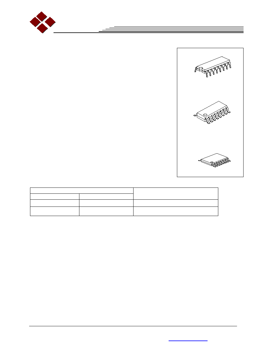
DIP16-P-300-2.54 Weight: 1.02g(typ)
MBI5001CD
MBI5168CD
SOP16-P-150-1.27 Weight: 0.13g(typ)
MBI5168CP
SSOP16-P-150-0.64 Weight: 0.07g(typ)

MBI5168
8-bit Constant Current LED Sink Driver
May
2003, V0.1
- 2 -
Terminal Description
PIN NO.
PIN NAME
FUNCTION
1
GND
Ground terminal for control logic and
current sink
2
SDI
Serial-data input to the shift register
3
CLK
Clock input terminal for data shift on
rising edge
4
LE
Data strobe input terminal
Serial data is transferred to the
respective latch when LE is high. The
data is latched when LE goes low.
5-12
OUT0 ~
7
OUT Constant current output terminals
13
OE
Output enable terminal
When (active) low, the output drivers
are enabled; when high, all output
drivers are turned OFF (blanked).
14
SDO
Serial-data output to the following SDI
of next driver IC
15
R-EXT
Input terminal used to connect an
external resistor for setting up output
current for all output channels
16
VDD
5V supply voltage terminal
Block Diagram
8-Bit Shift Register
8-Bit Output Latch
I
O
Regulator
8-Bit Output Driver
R-EXT
OE
LE
SDI
CLK
SDO
OUT7
OUT0
8
8
OUT1
VDD
GND
OUT6
Pin Description
9
10
11
12
13
14
15
16
SDO
R-EXT
VDD
OE
5
OUT
4
OUT
6
OUT
7
OUT
1
2
3
4
5
6
7
8
0
OUT
3
OUT
2
OUT
1
OUT
CLK
LE
SDI
GND

MBI5168
8-bit Constant Current LED Sink Driver
May
2003, V0.1
- 5 -
Truth Table
CLK
LE
OE
SDI
OUT0
...
OUT5
...
7
OUT
SDO
H
L
D
n
n
D
...
..
5
-
n
D
...
.
7
-
n
D
D
n-7
L
L
D
n+1
No Change
D
n-6
H
L
D
n+2
2
+
n
D
...
.
3
-
n
D
...
.
5
-
n
D
D
n-5
X
L
D
n+3
2
+
n
D
...
.
3
-
n
D
...
.
5
-
n
D
D
n-5
X
H
D
n+3
Off
D
n-5
Maximum Ratings
CHARACTERISTIC
SYMBOL
RATING
UNIT
Supply Voltage
V
DD
0~7.0
V
Input Voltage
V
IN
-0.4~V
DD
+ 0.4
V
Output Current
I
OUT
+120
mA
Output Voltage
V
DS
-0.5~+20.0
V
Clock Frequency
F
CLK
25
MHz
GND Terminal Current
I
GND
960
mA
CN
≠
type
1.64
CD
≠
type
1.06
Power Dissipation
(On PCB, Ta=25
∞
C)
CP
≠
type
P
D
0.88
W
CN
≠
type
76
CD
≠
type
117
Thermal Resistance
(On PCB, Ta=25
∞
C)
CP
≠
type
R
th(j-a)
141
∞
C/W
Operating Temperature
T
opr
-40~+85
∞
C
Storage Temperature
T
stg
-55~+150
∞
C

