2N3906
PNP General
Purpose Amplifier
TO-92
Features
∑
Through Hole Package
∑
Capable of 600mWatts of Power Dissipation
Electrical Characteristics @ 25
∞
C Unless Otherwise Specified
Symbol
Parameter
Min
Max
Units
OFF CHARACTERISTICS
V
(BR)CEO
Collector-Emitter Breakdown Voltage*
(I
C
=1.0mAdc, I
B
=0)
40
Vdc
V
(BR)CBO
Collector-Base Breakdown Voltage
(I
C
=10
µ
Adc, I
E
=0)
40
Vdc
V
(BR)EBO
Emitter-Base Breakdown Voltage
(I
E
=10
µ
Adc, I
C
=0)
5.0
Vdc
I
BL
Base Cutoff Current
(V
CE
=30Vdc, V
BE
=3.0Vdc)
50
nAdc
I
CEX
Collector Cutoff Current
(V
CE
=30Vdc, V
BE
=3.0Vdc)
50
nAdc
ON CHARACTERISTICS
h
FE
DC Current Gain*
(I
C
=0.1mAdc, V
CE
=1.0Vdc)
(I
C
=1.0mAdc, V
CE
=1.0Vdc)
(I
C
=10mAdc, V
CE
=1.0Vdc)
(I
C
=50mAdc, V
CE
=1.0Vdc)
(I
C
=100mAdc, V
CE
=1.0Vdc)
60
80
100
60
30
300
V
CE(sat)
Collector-Emitter Saturation Voltage
(I
C
=10mAdc, I
B
=1.0mAdc)
(I
C
=50mAdc, I
B
=5.0mAdc)
0.25
0.4
Vdc
V
BE(sat)
Base-Emitter Saturation Voltage
(I
C
=10mAdc, I
B
=1.0mAdc)
(I
C
=50mAdc, I
B
=5.0mAdc)
0.65
0.85
0.95
Vdc
SMALL-SIGNAL CHARACTERISTICS
f
T
Current Gain-Bandwidth Product
(I
C
=10mAdc, V
CE
=20Vdc, f=100MHz)
250
MHz
C
obo
Output Capacitance
(V
CB
=5.0Vdec, I
E
=0, f=100MHz)
4.5
pF
C
ibo
Input Capacitance
(V
BE
=0.5Vdc, I
C
=0, f=100kHz)
10.0
pF
NF
Noise Figure
(I
C
=100
µ
Adc, V
CE
=5.0Vdc, R
S
=1.0k
f=10Hz to 15.7kHz)
4.0
dB
SWITCHING CHARACTERISTICS
t
d
Delay Time
(V
CC
=3.0Vdc, V
BE
=0.5Vdc
35
ns
t
r
Rise Time
I
C
=10mAdc, I
B1
=1.0mAdc)
35
ns
t
s
Storage Time
(V
CC
=3.0Vdc, I
C
=10mAdc
225
ns
t
f
Fall Time
I
B1
=I
B2
=1.0mAdc)
75
ns
*Pulse Width
300
µ
s, Duty Cycle
2.0%
DIMENSIONS
INCHES
MM
DIM
MIN
MAX
MIN
MAX
NOTE
A
.175
.185
4.45
4.70
B
.175
.185
4.46
4.70
C
.500
---
12.7
---
D
.016
.020
0.41
0.63
E
.135
.145
3.43
3.68
G
.095
.105
2.42
2.67
A
E
B
C
D
G
Pin Configuration
Bottom View
C B
E
www.
mccsemi
.com
omponents
21201 Itasca Street Chatsworth
!"#
$
% !"#
M C C
2N3906
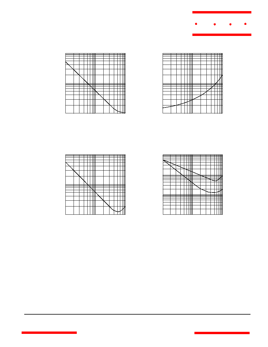
DC Current Gain vs Collector Current
h
FE
I
C
(mA)
40
80
120
160
200
220
0.1
1
10
100
Base-Emitter ON Voltage vs
Collector Current
V
BE(ON)
- (V)
I
C
- (mA)
0
0.2
0.4
0.6
0.8
1.0
1.2
0.1
1.0
10
100
Collector-Emitter Saturation
Volatge vs Collector Current
Base-Emitter Saturation
Voltage vs Collector Current
V
CE(SAT)
- (V)
V
BE(SAT)
- (V)
0
0.1
0.2
0.3
0.4
0.5
0.6
1.0
10
100
1000
0.2
0.4
0.6
0.8
1.0
1.2
1.4
1.0
10
100
1000
I
C
- (mA)
I
C
- (mA)
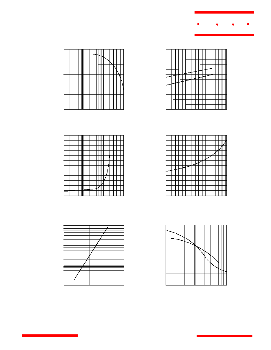
Collector-Base Diode Reverse
Current vs Temperature
Common Base Open Circuit Input and
Output Capacitance vs Reverse Bias Voltage
I
CBO
- (mA)
T
J
- (
∞
C)
Volts - (V)
pF
0.1
1.0
10
100
0
25
50
75
100 125
150
V
CB
= 20V
0
2
4
6
8
1.0
0.1
1.0
10
C
OBO
C
IBO
T
A
= 25
∞
C
TO-92
I
C
/I
B
= 10
T
A
= 25
∞
C
I
C
/I
B
= 10
T
A
= 25
∞
C
V
CE
= 1.0V
V
CE
= 5.0V
T
A
= 25
∞
C
T
A
= 100
∞
C
www.
mccsemi
.com
M C C
2N3906
f - (kHz)
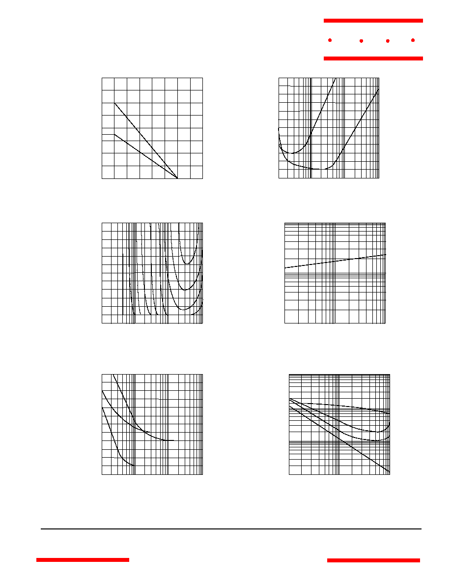
Maximum Power Dissipation vs
Ambient Temperature
Noise Figure vs
Source Resistance
P
D(MAX)
- (mW)
T
A
- (
∞
C)
TO-92
SOT-23
0
200
400
600
800
0
50
100
150
200
NF - (dB)
R
S
- (k
)
0
2
4
6
8
10
12
0.1
1.0
10
100
I
C
= 1.0mA
I
C
= 100
µ
A
V
CE
= 5.0V
f = 1.0kHz
Contours of Constant Gain
Bandwidth Product (f
T
)
Current Gain
V
CE
- (V)
I
C
- (mA)
h
fe
I
C
- (mA)
V
CE
= 10V
f = 1.0kHz
0
4
8
12
16
20
24
0.1
1.0
10
100
10
100
1000
0.1
1.0
10
Noise Figure vs
Frequency
Switching Times vs
Collector Current
NF - (dB)
T - (ns)
I
C
- (mA)
1.0
10
100
1000
1.0
10
100
I
B1
= I
B2
= I
C
/10
t
s
t
f
t
r
t
d
V
CE
= 5.0V
I
C
= 100
µ
A R
S
= 200
I
C
= 1.0mA R
S
= 200
I
C
= 100
µ
A R
S
= 2.0k
0.1
1.0
10
100
0
1
2
3
4
5
6
*100MHz increments from 100
to 700, 750 and 800MHz
www.
mccsemi
.com
M C C