Features
l
Ideally Suited for Automatic Insertion
l
150
o
C Junction Temperature
l
For Switching and AF Amplifier Applications
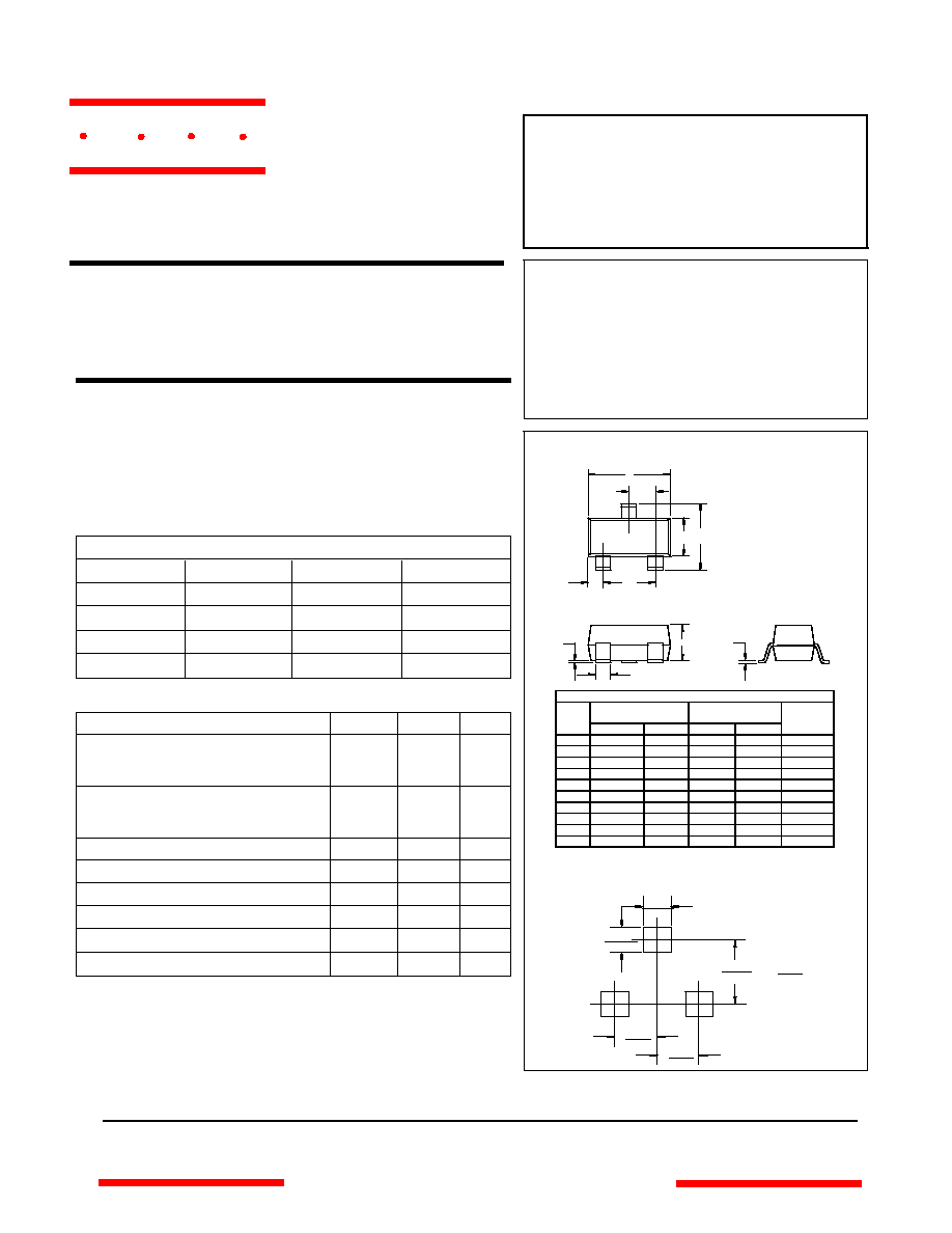
Mechanical Data
l
Case: SOT-23, Molded Plastic
l
Terminals: Solderable per MIL-STD-202, Method 208
l
Polarity: See Diagram
l
Weight: 0.008 grams ( approx.)
Type
Marking
Type
Marking
BC856A
3A
BC857C
3G
BC856B
3B
BC858A
3J
BC857A
3E
BC858B
3K
BC857B
3F
BC858C
3L
Marking Code (Note 2)
Maximum Ratings @ 25
o
C Unless Otherwise Specified
Charateristic
Symbol Value
Unit
Collector-Base Voltage BC856
BC857
BC858
V
CBO
-80
-50
-30
V
Collector-Emitter Voltage BC856
BC857
BC858
V
CEO
-65
-45
-30
V
Emitter-Base Voltage
V
EBO
-5.0
V
Collector Current
I
C
-100
mA
Peak Collector Current
I
C M
-200
mA
Peak Emitter Current
I
EM
-200
mA
Power Dissipation@T
s
=50
o
C(Note1)
P
d
310
mW
Operating & Storage Temperature
T
j
, T
STG
-55~150
o
C
Note:
1.
Package mounted on ceramic substrate 0.7mm X 2.5cm
2
area.
2.
Current gain subgroup "C" is not available for BC856
BC856A
THRU
BC858C
PNP Small
Signal Transistor
310mW
Suggested Solder
Pad Layout
DIMENSIONS
INCHES
MM
DIM
MIN
MAX
MIN
MAX
NOTE
A
.110
.120
2.80
3.04
B
.083
.098
2.10
2.64
C
.047
.055
1.20
1.40
D
.035
.041
.89
1.03
E
.070
.081
1.78
2.05
F
.018
.024
.45
.60
G
.0005
.0039
.013
.100
H
.035
.044
.89
1.12
J
.003
.007
.085
.180
K
.015
.020
.37
.51
A
B
C
D
E
F
G
H
J
.079
2.000
inches
mm
.031
.800
.035
.900
.037
.950
.037
.950
SOT-23
www.
mccsemi
.com
omponents
21201 Itasca Street Chatsworth
!"#
$
% !"#
M C C
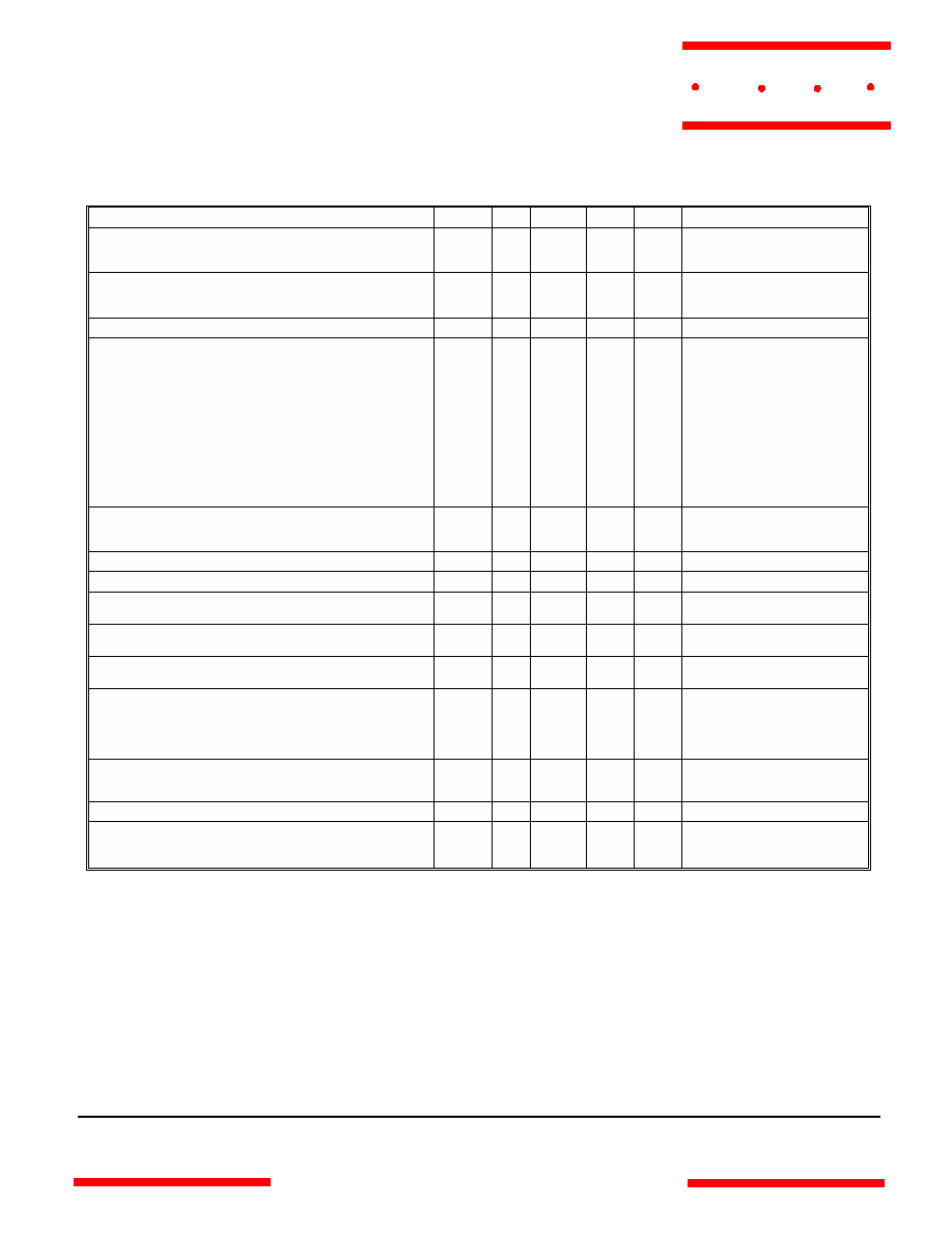
Electrical Characteristics
Characteristic
Symbol Min
Typ
Max
Unit
Test Condition
Collector-Base Breakdown Voltage (Note 3) BC856
BC857
BC858
V
(BR)CBO
-80
-50
-30
--
--
--
--
--
--
V
I
C
= 10mA, I
B
= 0
Collector-Emitter Breakdown Voltage (Note 3) BC856
BC857
BC858
V
(BR)CEO
-65
-45
-30
--
--
--
--
--
--
V
I
C
= 10mA, I
B
= 0
Emitter-Base Breakdown Voltage (Note 3)
V
(BR)EBO
-5
--
--
V
I
E
= 1mA, I
C
= 0
H-Parameters
Small Signal Current Gain
Current Gain Group A
B
C
Input Impedance
Current Gain Group A
B
C
Output Admittance
Current Gain Group A
B
C
Reverse Voltage Transfer Ratio
Current Gain Group A
B
C
h
fe
h
fe
h
fe
h
ie
h
ie
h
ie
h
oe
h
oe
h
oe
h
re
h
re
h
re
--
--
--
--
--
--
--
--
--
--
--
--
200
330
600
2.7
4.5
8.7
18
30
60
1.5x10
-4
2x10
-4
3x10
-4
--
--
--
--
--
--
--
--
--
--
--
--
--
--
--
kW
kW
kW
µS
µS
µS
--
--
--
V
CE
= -5.0V, I
C
= -2.0mA,
f = 1.0kHz
DC Current Gain (Note 3)
Current Gain Group A
B
C
h
FE
125
220
420
180
290
520
250
475
800
--
V
CE
= -5.0V, I
C
= -2.0mA
Thermal Resistance, Junction to Substrate Backside
R
qJSB
--
--
320
∞C/W
Note 1
Thermal Resistance, Junction to Ambient
R
qJA
--
--
400
∞C/W
Note 1
Collector-Emitter Saturation Voltage (Note 3)
V
CE(SAT)
--
-75
-250
-300
-650
mV
I
C
= -10mA, I
B
= -0.5mA
I
C
= -100mA, I
B
= -5.0mA
Base-Emitter Saturation Voltage (Note 3)
V
BE(SAT)
--
--
-700
-850
--
mV
I
C
= -10mA, I
B
= -0.5mA
I
C
= -100mA, I
B
= -5.0mA
Base-Emitter Voltage (Note 3)
V
BE(ON)
-600
--
-650
--
-750
-820
mV
V
CE
= -5.0V, I
C
= -2.0mA
V
CE
= -5.0V, I
C
= -10mA
Collector-Cutoff Current (Note 3) BC856
BC857
BC858
I
CES
I
CES
I
CES
I
CBO
I
CBO
--
--
--
--
--
--
--
--
--
--
-15
-15
-15
-15
-4.0
nA
nA
nA
nA
µA
V
CE
= -80V
V
CE
= -50V
V
CE
= -30V
V
CB
= -30V
V
CB
= -30V, T
A
= 150∞C
Gain Bandwidth Product
f
T
100
200
--
MHz
V
CE
= -5.0V, I
C
= -10mA,
f = 100MHz
Collector-Base Capacitance
C
CBO
--
3
--
pF
V
CB
= -10V, f = 1.0MHz
Noise Figure
NF
--
2
10
dB
V
CE
= -5.0V, I
C
= 200µA,
R
S
= 2kW, f = 1kHz,
Df = 200Hz
Notes:
1. Package mounted on ceramic substrate 0.7mm x 2.5cm
2
area.
2. Current gain subgroup "C" is not available for BC856.
3. Short duration pulse test to minimize self-heating effect.
@ T
A
=25∞C unless otherwise specified
www.
mccsemi
.com
M C C
BC856A thru BC858C