Features
l
Low Reverse Recovery Time
l
Low Reverse Capacitance
l
Low Forward Voltage Drop
l
Guard Ring Construction for Transient Protection
Mechanical Data
l
Case: MiniMELF, Glass
l
Terminals: Solderable per MIL -STD-202, Method 208
l
Polarity: Indicated by Cathode Band
l
Weight: 0.05 grams ( approx.)
Maximum Ratings @ 25
o
C Unless Otherwise Specified
Characteristic
Symbol LLSD101A LLSD101B LLSD101C
Peak Repetitive Reverse Voltage
Working Peak Reverse Voltage
DC Blocking Voltage
V
RRM
V
RWM
V
R
60V
50V
40V
RMS Reverse Voltage
V
R(RMS)
42V
35V
28V
Forward Continuous Current(Note 1)
I
FM
15mA
Non-Repetitive Peak @ t<=1.0s
Forward Surge Current @ t=10us
I
FSM
50mA
2.0A
Power Dissipation(Note 1)
Pd
400mW
Thermal Resistance(Note 1)
R
375K/W
Operation & Storage Temp. Range
Tj, T
STG
-55 to 150
o
C
Electrical Characteristics @ 25
o
C Unless Otherwise Specified
Charateristic
Symbol Min
Max Unit
Test Cond.
Peak LLSD101A
V
R
=50V
Reverse LLSD101B
I
R M
-----
200
nA V
R
=40V
Current LLSD101C
V
R
=30V
LLSD101A
0.41
I
F
=1.0mA
LLSD101B
0.40
I
F
=1.0mA
Forward LLSD101C
V
F M
-----
0.39
V
I
F
=1.0mA
Volt. Drop LLSD101A
1.00
I
F
=15mA
LLSD101B
0.95
I
F
=15mA
LLSD101C
0.90
I
F
=15mA
Junction LLSD101A
2.0
Capacitance LLSD101B
Cj
-----
2.1
pF V
R
=0V, f=1.0MHz
LLSD101C
2.2
Reverse Recovery Time
t
rr
-----
1.0
ns
I
F
= I
R
=5mA,
recover to 0.1 I
R
Note
: 1. Valid provided that electrodes are kept at ambient temperature
LLSD101A
THRU
LLSD101C
Schottky Barrier
Switching Diode
www.
mccsemi
.com
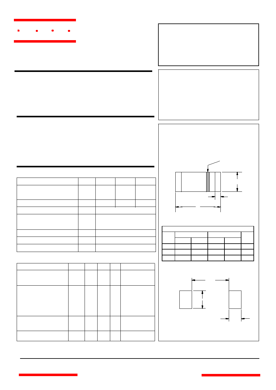
DIMENSION
INCHES
MM
DIM
MIN
MAX
MIN
MAX
NOTE
A .134 .142 3.40 3.60
B .008 .016 .20 .40
C .055 .059 1.40 1.50
MINIMELF
A
B
C
Cathode Mark
0.030"
0.105
0.075"
SUGGESTED SOLDER
PAD LAYOUT
omponents
21201 Itasca Street Chatsworth
!"#
$
% !"#
M C C
LLSD101A thru LLSD101C
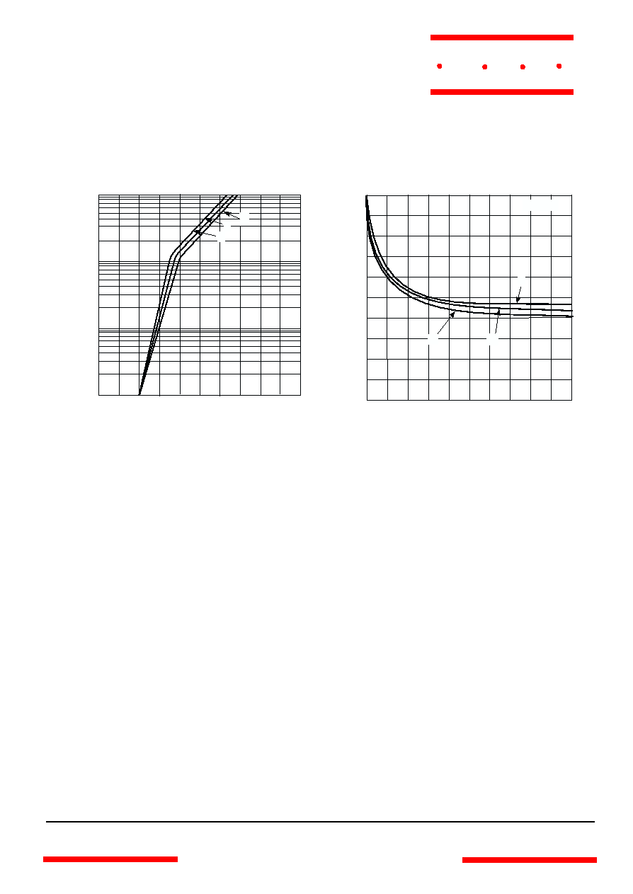
0.01
0.1
1.0
10
0
0.5
1.0
I
,
FOR
W
ARD
CURRENT
(mA)
F
A
B
C
V , FORWARD VOLTAGE (V)
Fig. 1 Typical Forward Characteristic
Variations for Primary Conduction
F
0
1
2
0
10
20
30
40
50
C
,
CAP
ACIT
ANCE
(pF)
j
V , REVERSE VOLTAGE (V)
R
Fig. 2 Typ. Junction Capacitance vs Reverse Voltage
T = 25 C
j
∞
A
B
C
M C C
www.
mccsemi
.com