DESCRIPTION (500 watt)
This TRANSIENT VOLTAGE SUPPRESSOR (TVS) array is packaged
in an SO-8 configuration giving protection to 2 Bidirectional data or
interface lines. It is designed for use in applications where protection
is required at the board level from voltage transients caused by
electrostatic discharge (ESD) as defined in IEC 1000-4-2, electrical
fast transients (EFT) per IEC 1000-4-4 and effects of secondary
lighting.
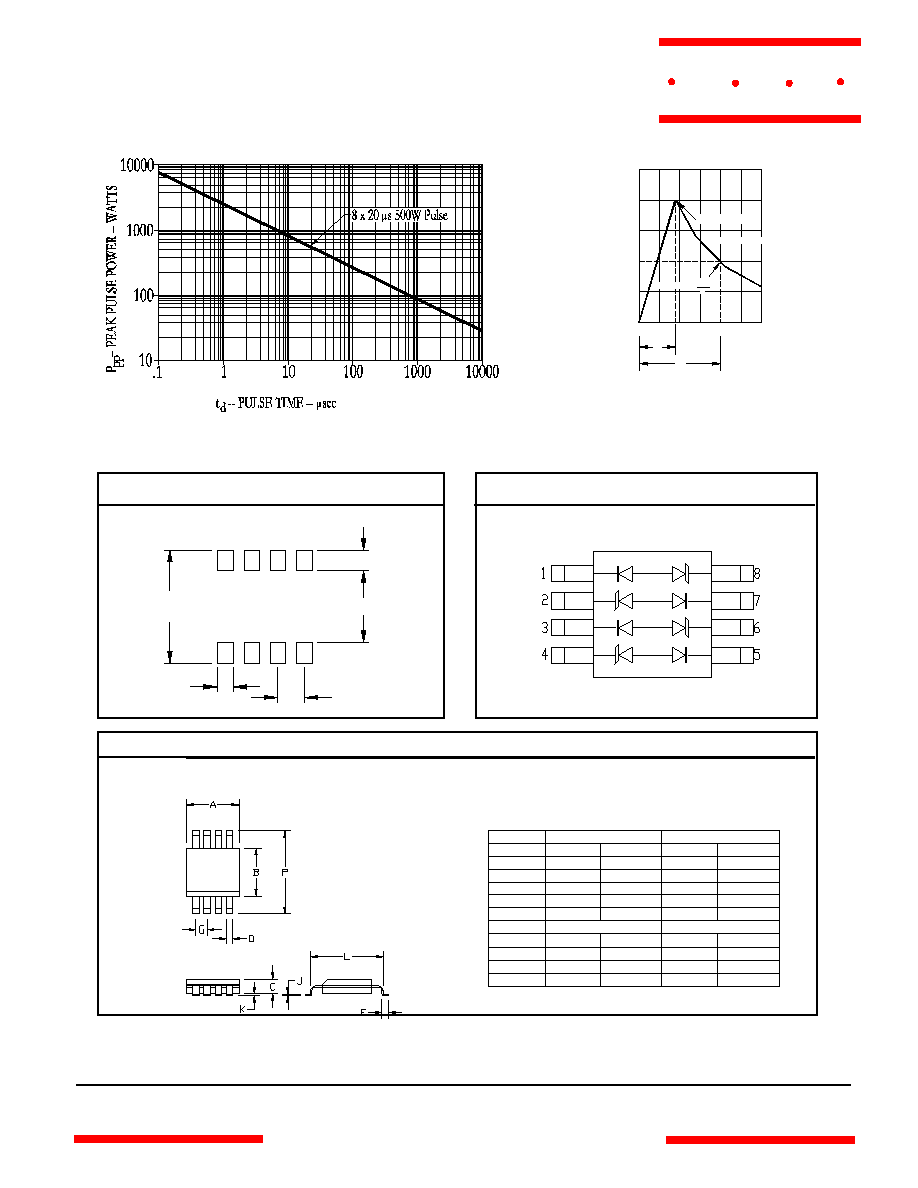
These TVS arrays have a peak power rating of 500 watts for an
8/20
µ
sec pulse. This array is suitable for protection of sensitive
circuitry consisting of TTL, CMOS DRAM's, SRAM's, HCMOS, HSIC
microprocessors, UNIVERSAL SERIAL BUS (USB) and I/O
transceivers. The USB08XXC product provides board level protection from static electricity and other
induced voltage surges that can damage or upset sensitive circuitry.
FEATURES
MECHANICAL
∑
Protects up to 2 Bidirectional lines
∑
Molded SO-8 Surface Mount
∑
Surge protection Per IEC 1000-4-2, IEC 1000-4-4
∑
Weight: 0.066 grams (approximate)
∑
Provides electrically isolated protection
∑
Marking: Logo, device number, date code
∑
SO-8 Packaging
∑
Pin #1 defined by DOT on top of package
∑
ULTRA LOW CAPACITANCE 5 pF per line pair
∑
ULTRA LOW LEAKAGE
MAXIMUM RATINGS
PACKAGING
∑
Operating Temperatures: -55
0
C to +150
0
C
∑
Tape & Reel EIA Standard 481-1-A
∑
Storage Temperature: -55
0
C to +150
0
C
∑
13 inch reel 2,500, pieces (OPTIONAL)
∑
Peak Pulse Power: 500 Watts (8/20
µ
sec, Figure 1)
∑
Carrier tubes 95 pcs per (STANDARD)
∑
Pulse Repetition Rate: <.01%
ELECTRICAL CHARACTERISTICS PER LINE @ 25
0
C Unless otherwise specified
STAND
OFF
VOLTAGE
V
WM
VOLTS
BREAKDOWN
VOLTAGE
V
BR
@1 mA
VOLTS
CLAMPING
VOLTAGE
V
C
@ 1 Amp
(FIGURE 2)
VOLTS
CLAMPING
VOLTAGE
V
C
@ 5 Amp
(FIGURE 2)
VOLTS
LEAKAGE
CURRENT
I
D
@ V
WM
µA
CAPACITANCE
(f=1 MHz)
@0V
C
pF
TEMPERATURE
COEFFICIENT
OF V
BR
·
VBR
mV/∞C
PART
NUMBER
DEVICE
MARKING
MIN MAX MAX MAX MAX MAX
USB0803C
U3C
3.3
4
7
11
200
5
-5
USB0805C
U5C
5.0
6.0
9.8
13
40
5
1
USB0812C
U12C
12.0
13.3
19
26
1
5
8
USB0815C
U15C
15.0
16.7
24
32
1
5
11
USB0824C
U24C
24.0
26.7
43
57
1
5
28
NOTE: TVS product is normally selected based on its stand off Voltage V
WM
. Product selected voltage should be
equal to or greater than the continuous peak operating voltage of the circuit to be protected.
Application: The USB08XXC product is designed for transient voltage suppression protection of ESD sensitive
components at the board level. It is an ideal product to be used for protection of I/O Transceivers.
USB0803C
THRU
USB0824C
TVSarray
TM
TM
Series
www.
mccsemi
.com
omponents
21201 Itasca Street Chatsworth
!"#
$
% !"#
M C C