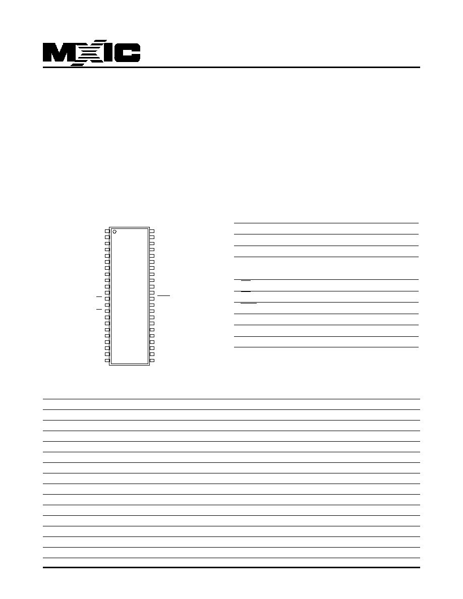
PIN DESCRIPTION
Symbol
Pin Function
A0~A20
Address Inputs
D0~D14
Data Outputs
D15/A-1
D15 (Word Mode)/ LSB Address
(Byte Mode)
CE
Chip Enable Input
OE
Output Enable Input
Byte
Word/ Byte Mode Selection
VCC
Power Supply Pin
VSS
Ground Pin
NC
No Connection
1
P/N:PM0411
REV. 2.9, MAY 11, 2004
32M-BIT MASK ROM (8/16-BIT OUTPUT)
FEATURES
∑ Bit organization
- 4M x 8 (byte mode)
- 2M x 16 (word mode)
∑ Fast access time
- Random access: 70ns (max.)
- Page access: 25ns (max.)
∑ Page Size
- 8 words per page
ORDER INFORMATION
Part No.
Access Time
Page Access Time
Package
Remark
MX23L3211MC-70
70ns
25ns
44 pin SOP
MX23L3211MC-90
90ns
25ns
44 pin SOP
MX23L3211MC-10
100ns
30ns
44 pin SOP
MX23L3211MC-12
120ns
50ns
44 pin SOP
MX23L3211MC-10G
100ns
30ns
44 pin SOP
Pb-free
MX23L3211MC-12G
120ns
50ns
44 pin SOP
Pb-free
MX23L3211TC-90
90ns
25ns
48 pin TSOP
MX23L3211TC-10
100ns
30ns
48 pin TSOP
MX23L3211TC-12
120ns
50ns
48 pin TSOP
MX23L3211TC-10G
100ns
30ns
48 pin TSOP
Pb-free
MX23L3211TC-12G
120ns
50ns
48 pin TSOP
Pb-free
MX23L3211RC-90
90ns
25ns
48 pin TSOP(Reverse type)
MX23L3211RC-10
100ns
30ns
48 pin TSOP(Reverse type)
MX23L3211RC-12
120ns
50ns
48 pin TSOP(Reverse type)
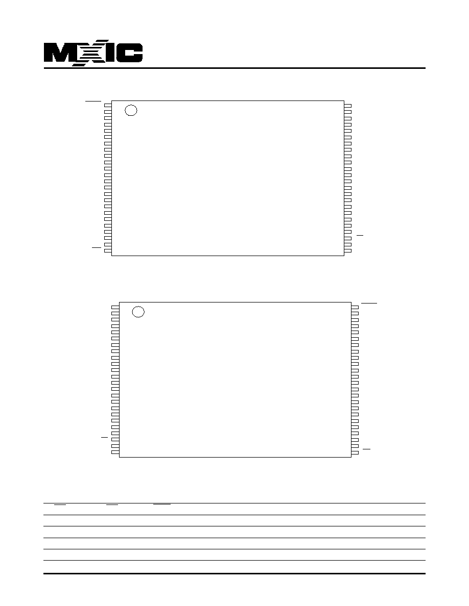
PIN CONFIGURATION
44 SOP
MX23L3211
2
3
4
5
6
7
8
9
10
11
12
13
14
15
16
17
18
19
20
21
22
44
43
42
41
40
39
38
37
36
35
34
33
32
31
30
29
28
27
26
25
24
23
NC
A18
A17
A7
A6
A5
A4
A3
A2
A1
A0
CE/CE
VSS
OE/OE
D0
D8
D1
D9
D2
D10
D3
D11
A20
A19
A8
A9
A10
A11
A12
A13
A14
A15
A16
BYTE
VSS
D15/A1
D7
D14
D6
D13
D5
D12
D4
VCC
MX23L3211
∑ Current
- Operating:40mA
- Standby:5uA
∑ Supply voltage
- 3.0V ~ 3.6V for 90ns and 70ns speed grades
- 2.7V ~ 3.6V for 100ns and 120ns speed grades
∑ Package
- 44 pin SOP (500mil)
- 48 pin TSOP (12mm x 20mm)
2
P/N:PM0411
REV. 2.9, MAY 11, 2004
MX23L3211
48 TSOP (Normal Type)
48 TSOP (Reverse Type)
BYTE
A16
A15
A14
A13
A12
A11
A10
A9
A8
A19
VSS
A20
A18
A17
A7
A6
A5
A4
A3
A2
A1
A0
CE
1
2
3
4
5
6
7
8
9
10
11
12
13
14
15
16
17
18
19
20
21
22
23
24
VSS
VSS
D15/A-1
D7
D14
D6
D13
D5
D12
D4
VCC
VCC
NC
D11
D3
D10
D2
D9
D1
D8
D0
OE
VSS
VSS
48
47
46
45
44
43
42
41
40
39
38
37
36
35
34
33
32
31
30
29
28
27
26
25
MX23L3211
(Normal Type)
BYTE
A16
A15
A14
A13
A12
A11
A10
A9
A8
A19
VSS
A20
A18
A17
A7
A6
A5
A4
A3
A2
A1
A0
CE
48
47
46
45
44
43
42
41
40
39
38
37
36
35
34
33
32
31
30
29
28
27
26
25
VSS
VSS
D15/A-1
D7
D14
D6
D13
D5
D12
D4
VCC
VCC
NC
D11
D3
D10
D2
D9
D1
D8
D0
OE
VSS
VSS
1
2
3
4
5
6
7
8
9
10
11
12
13
14
15
16
17
18
19
20
21
22
23
24
MX23L3211
(Reverse Tpye)
MODE SELECTION
CE
OE
Byte
D15/A-1
D0~D7
D8~D15
Mode
Power
H
X
X
X
High Z
High Z
-
Stand-by
L
H
X
X
High Z
High Z
-
Active
L
L
H
Output
D0~D7
D8~D15
Word
Active
L
L
L
Input
D0~D7
High Z
Byte
Active
3
P/N:PM0411
REV. 2.9, MAY 11, 2004
MX23L3211
ABSOLUTE MAXIMUM RATINGS
Item
Symbol
Ratings
Supply Voltage Relative to VSS
VCC
-0.3V to 4.3V
Voltage on any Pin Relative to VSS
VIN
-0.5V to VCC + 2.0V
Ambient Operating Temperature
Topr
0
∞
C to 70
∞
C
Storage Temperature
Tstg
-65
∞
C to 125
∞
C
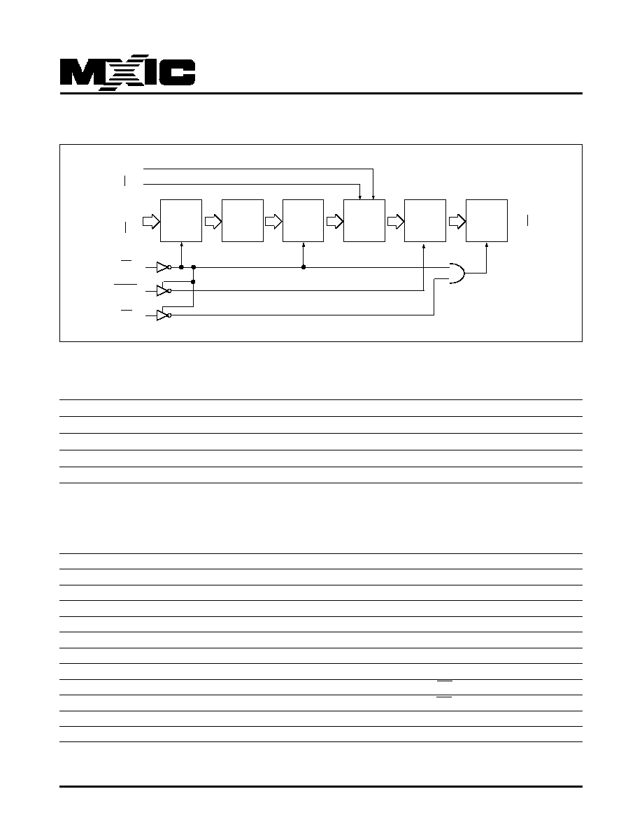
BLOCK DIAGRAM
DC CHARACTERISTICS (Ta = 0
∞
C ~ 70
∞
C, VCC = 2.7V~3.6V)
Item
Symbol
MIN.
MAX.
Conditions
Output High Voltage
VOH
2.4V
-
IOH = -400uA
Output Low Voltage
VOL
-
0.4V
IOL = 1.6mA
Input High Voltage
VIH
2.2V
VCC+0.3V
Input Low Voltage
VIL
-0.3V
0.8V
Input Leakage Current
ILI
-
5uA
0V, VCC
Output Leakage Current
ILO
-
5uA
0V, VCC
Operating Current
ICC1
-
40mA
tRC = 100ns, all output open
Standby Current (TTL)
ISTB1
-
1mA
CE = VIH
Standby Current (CMOS)
ISTB2
-
5uA
CE>VCC-0.2V
Input Capacitance
CIN
-
10pF
Ta = 25
∞
C, f = 1MHZ
Output Capacitance
COUT
-
10pF
Ta = 25
∞
C, f = 1MHZ
Address
Buffer
Memory
Array
Page
Buffer
Page
Decoder
Word/
Byte
Output
Buffer
D0
D15/(D7)
A3
A20
A0/(A-1)
A2
CE
BYTE
OE
4
P/N:PM0411
REV. 2.9, MAY 11, 2004
MX23L3211
AC CHARACTERISTICS (Ta = 0
∞
C ~ 70
∞
C, VCC =2.7V~3.6V)
Item
Symbol
23L3211-70*
23L3211-90
23L3211-10
23L3211-12
MIN.
MAX.
MIN.
MAX.
MIN.
MAX.
MIN.
MAX.
Read Cycle Time
tRC
70ns
-
90ns
-
100ns
-
120ns
-
Address Access Time
tAA
-
70ns
-
90ns
-
100ns
-
120ns
Chip Enable Access Time
tACE
-
70ns
-
90ns
-
100ns
-
120ns
Page Mode Access Time
tPA
-
25ns
-
25ns
-
30ns
-
50ns
Output Enable Time
tOE
-
25ns
-
25ns
-
30ns
-
50ns
Output Hold After Address
tOH
0ns
-
0ns
-
0ns
-
0ns
-
Output High Z Delay
tHZ*
-
20ns
-
20ns
-
20ns
-
20ns
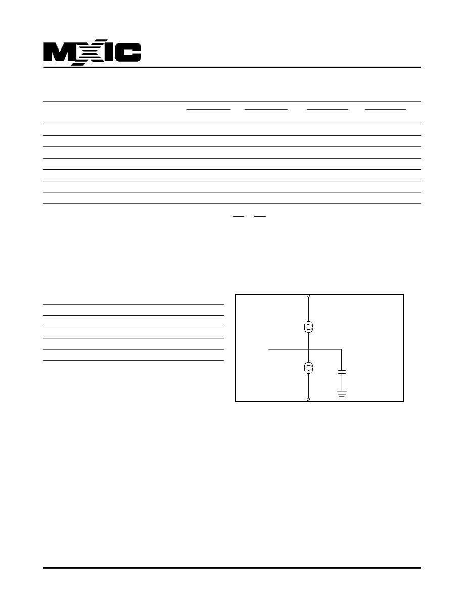
AC Test Conditions
Input Pulse Levels
0.4V~ 2.6V
Input Rise and Fall Times
10ns
Input Timing Level
1.4V
Output Timing Level
1.4V
Output Load
See Figure
Note:
No output loading is present in tester load board.
Active loading is used and under software programming control.
Output loading capacitance includes load board's and all stray capacitance.
DOUT
C<100pF
IOL (load)=1.6mA
IOH (load)=-0.4mA
Note:
1. Output high-impedance delay (tHZ) is measured from OE or CE going high, and this parameter guaranteed by
design over the full voltage and temperature operating range - not tested.
2. For 70ns speed grade, the VCC range is 3.0~3.6V, operating temperature 0~55
∞
C, and output load is 30pF.
5
P/N:PM0411
REV. 2.9, MAY 11, 2004
MX23L3211
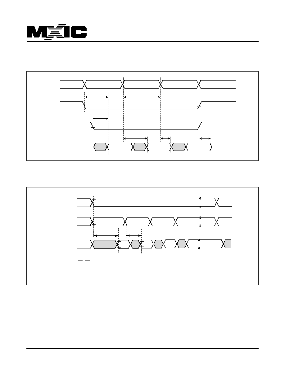
TIMING DIAGRAM
RANDOM READ
PAGE READ
tACE
tAA
tOH
tHZ
ADD
ADD
ADD
ADD
CE
OE
DATA
VALID
VALID
VALID
tRC
tOE
A3-A20
(A-1),A0,A1,A2
DATA
Note: CE, OE are enable.
Page size is 8 words in 16-bit mode, 16 bytes in 8-bit mode.
VALID ADD
VALID
1'st ADD
2'nd ADD
tPA
tAA
3'rd ADD
VALID
VALID