
1
P/N:PM0716
REV. 1.7 ,JUN. 29, 2005
FEATURES
∑ Bit organization
- 4M x 8 (byte mode)
- 2M x 16 (word mode)
∑ Fast access time
- Random access:70ns(max.)
∑ Current
- Operating:16mA
- Standby:5uA
∑ Supply voltage
- 2.7V ~ 3.6V
∑ Package
- 48 pin TSOP (12mm x 20mm)
∑ Temperature
- -40 ~ 85
∞
C
PIN DESCRIPTION
Symbol
Pin Function
A0~A20
Address Inputs
D0~D14
Data Outputs
D15/A-1
D15 (Word Mode)/ LSB Address
(Byte Mode)
CE#
Chip Enable Input
OE#
Output Enable Input
Byte#
Word/ Byte Mode Selection
VCC
Power Supply Pin
VSS
Ground Pin
NC
No Connection
PIN CONFIGURATION
48 TSOP (Top View)
MX23L3213
32M-BIT MASK ROM
A15
A14
A13
A12
A11
A10
A9
A8
A19
A20
NC
NC
NC
NC
NC
A18
A17
A7
A6
A5
A4
A3
A2
A1
1
2
3
4
5
6
7
8
9
10
11
12
13
14
15
16
17
18
19
20
21
22
23
24
A16
BYTE#
VSS
D15/A-1
D7
D14
D6
D13
D5
D12
D4
VCC
D11
D3
D10
D2
D9
D1
D8
D0
OE#
VSS
CE#
A0
48
47
46
45
44
43
42
41
40
39
38
37
36
35
34
33
32
31
30
29
28
27
26
25
MX23L3213
(Normal Type)
MODE SELECTION
CE#
OE#
Byte#
D15/A-1
D0~D7
D8~D15
Mode
Power
H
X
X
X
High Z
High Z
-
Stand-by
L
H
X
X
High Z
High Z
-
Active
L
L
H
Output
D0~D7
D8~D15
Word
Active
L
L
L
Input
D0~D7
High Z
Byte
Active
2
P/N:PM0716
REV. 1.7, JUN. 29, 2005
MX23L3213
ABSOLUTE MAXIMUM RATINGS
Item
Symbol
Ratings
Voltage on any Pin Relative to VSS
VIN
-0.3V to 3.9V
Ambient Operating Temperature
Topr
-40
∞
C to 85
∞
C
Storage Temperature
Tstg
-65
∞
C to 125
∞
C
DC CHARACTERISTICS (Ta = -40
∞
C ~ 85
∞
C, VCC = 2.7V~3.6V)
Item
Symbol
MIN.
MAX.
Conditions
Output High Voltage
VOH
2.4V
-
IOH = -400uA
Output Low Voltage
VOL
-
0.4V
IOL = 1.6mA
Input High Voltage
VIH
2.2V
VCC+0.3V
Input Low Voltage
VIL
-0.3V
0.8V
Input Leakage Current
ILI
-
5uA
0V, VCC
Output Leakage Current
ILO
-
5uA
0V, VCC
Operating Current
ICC
-
16mA
f=5MHz, CE#=VIL, OE#=VIH
all output open
Standby Current (CMOS)
ISTB
-
5uA
CE#>VCC-0.2V
Input Capacitance
CIN
-
10pF
Ta = 25
∞
C, f = 1MHZ
Output Capacitance
COUT
-
10pF
Ta = 25
∞
C, f = 1MHZ
ORDER INFORMATION
Part No.
Speed
Package
Grade
Remark
MX23L3213TC-70
70ns
48 pin TSOP
Commercial
MX23L3213TC-90
90ns
48 pin TSOP
Commercial
MX23L3213TC-12
120ns
48 pin TSOP
Commercial
MX23L3213TI-70
70ns
48 pin TSOP
Industrial
MX23L3213TI-90
90ns
48 pin TSOP
Industrial
MX23L3213TI-10
100ns
48 pin TSOP
Industrial
MX23L3213TI-12
120ns
48 pin TSOP
Industrial
MX23L3213TC-90G
90ns
48 pin TSOP
Commercial
Pb-free, RoHS
MX23L3213TC-10G
100ns
48 pin TSOP
Commercial
Pb-free, RoHS
MX23L3213TI-90G
90ns
48 pin TSOP
Industrial
Pb-free, RoHS
MX23L3213TI-12G
120ns
48 pin TSOP
Industrial
Pb-free, RoHS
Note: Industrial grade temperature: -40 ~ 85
∞
C
Commercial grade temperature: 0 ~ 70
∞
C
3
P/N:PM0716
REV. 1.7, JUN. 29, 2005
MX23L3213
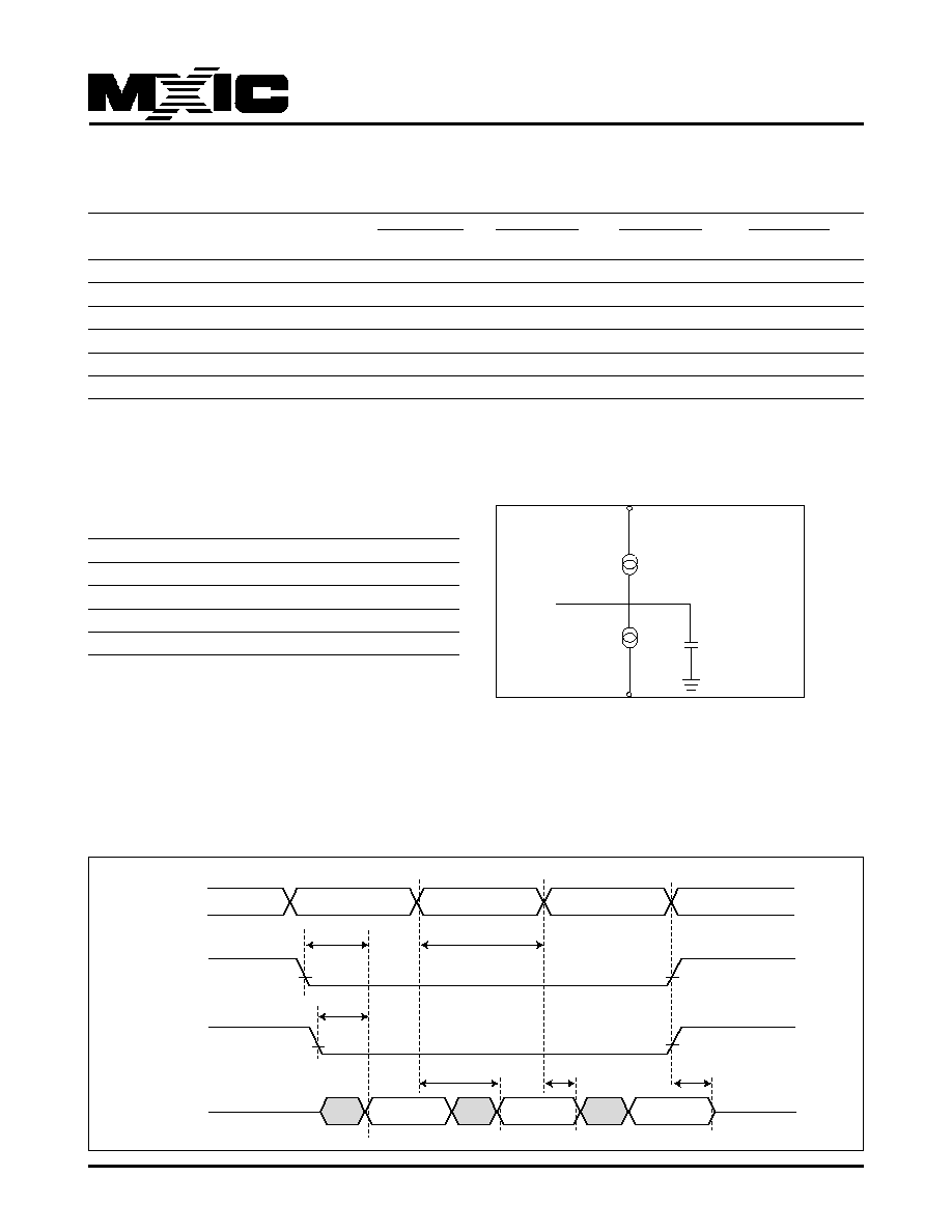
AC Test Conditions
Input Pulse Levels
0V~ 3.0V
Input Rise and Fall Times
5ns
Input Timing Level
1.5V
Output Timing Level
1.5V
Output Load
See Figure
Note:No output loading is present in tester load board.
Active loading is used and under software programming control.
Output loading capacitance includes load board's and all stray capacitance.
DOUT
C<100pF
IOL (load)=1.6mA
IOH (load)=-0.4mA
TIMING DIAGRAM
RANDOM READ
Note:
30pF output load capacitance for 70 and 90ns
speed grade
100pF output load capacitance for 120ns speed
grade
tACE
tAA
tOH
tHZ
ADD
ADD
ADD
ADD
CE#
OE#
DATA
VALID
VALID
VALID
tRC
tOE
AC CHARACTERISTICS (Ta = -40
∞
C ~ 85
∞
C, VCC = 2.7V~3.6V)
Item
Symbol
23L3213-70
23L3213-90
23L3213-10
23L3213-12
MIN.
MAX.
MIN.
MAX.
MIN.
MAX.
MIN.
MAX.
Read Cycle Time
tRC
70ns
-
90ns
-
100ns
-
120ns
-
Address Access Time
tAA
-
70ns
-
90ns
-
100ns
-
120ns
Chip Enable Access Time
tACE
-
70ns
-
90ns
-
100ns
-
120ns
Output Enable Time
tOE
-
30ns
-
40ns
-
40ns
-
50ns
Output Hold After Address
tOH
0ns
-
0ns
-
0ns
-
0ns
-
Output High Z Delay
tHZ
-
20ns
-
20ns
-
20ns
-
20ns
Note:Output high-impedance delay (tHZ) is measured from OE# or CE# going high, and this parameter guaranteed
by design over the full voltage and temperature operating range - not tested.
4
P/N:PM0716
REV. 1.7, JUN. 29, 2005
MX23L3213
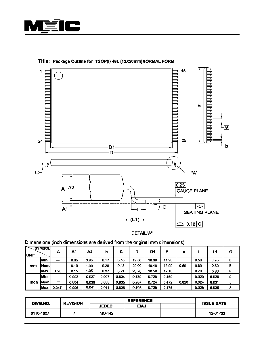
PACKAGE INFORMATION

5
P/N:PM0716
REV. 1.7, JUN. 29, 2005
MX23L3213
REVISION HISTORY
Revision No. Description
Page
Date
1.1
Modify DC Characteristics VOH:2.3-->2.4 ; VIH:2.1-->2.2
P3
JAN/04/2001
1.2
1.Modify Pin Configuration-- 48 mini BGA
P1,2
JUL/05/2001
2.Added 48-Ball mini BGA--Pckage Information
P6
1.3
Added Order Information
P2
JUL/16/2001
Add Tempetature:-40~85
∞
C
P1
1.4
Add CE#=VIL, OE#=VIH in DC Characteristics's ICC
P3
OCT/03/2001
1.5
Modify Package Information
P5,6
NOV/22/2002
1.6
Deleted 48-ball CSP package
P1,2
JUL/07/2004
1.7
Added access time: 100ns
P2,3
JUN/29/2005