1
MX29F004T/B
4M-BIT [512KX8] CMOS FLASH MEMORY
FEATURES
∑ 524,288 x 8 only
∑ Single power supply operation
- 5.0V only operation for read, erase and program op-
eration
∑ Fast access time: 70/90/120ns
∑ Low power consumption
- 30mA maximum active current (5MHz)
- 1uA typical standby current
∑ Command register architecture
- Byte Programming (7us typical)
- Sector Erase
(Sector structure:16KB/8KB/8KB/32KB and 64KBx7)
∑ Auto Erase (chip & sector) and Auto Program
- Automatically erase any combination of sectors with
Erase Suspend capability.
- Automatically program and verify data at specified
address
during erase and programming, while maintaining maxi-
mum EPROM compatibility.
MXIC Flash technology reliably stores memory
contents even after 100,000 erase and program
cycles. The MXIC cell is designed to optimize the
erase and programming mechanisms. In addition,
t h e c o m b i n a t i o n o f a d v a n c e d t u n n e l o x i d e
processing and low internal electric fields for erase
and program operations produces reliable cycling.
The MX29F004T/B uses a 5.0V
±
10% VCC supply
to perform the High Reliability Erase and auto
Program/Erase algorithms.
The highest degree of latch-up protection is
achieved with MXIC's proprietary non-epi process.
Latch-up protection is proved for stresses up to 100
milliamps on address and data pin from -1V to VCC
+ 1V.
GENERAL DESCRIPTION
The MX29F004T/B is a 4-mega bit Flash memory orga-
nized as 512K bytes of 8 bits. MXIC's Flash memories
offer the most cost-effective and reliable read/write non-
volatile random access memory. The MX29F004T/B is
packaged in 32-pin PLCC, TSOP, PDIP. It is designed
to be reprogrammed and erased in system or in stan-
dard EPROM programmers.
The standard MX29F004T/B offers access time as fast
as 70ns, allowing operation of high-speed microproces-
sors without wait states. To eliminate bus contention,
the MX29F004T/B has separate chip enable (CE) and
output enable (OE) controls.
MXIC's Flash memories augment EPROM functionality
with in-circuit electrical erasure and programming. The
MX29F004T/B uses a command register to manage this
functionality. The command register allows for 100%
TTL level control inputs and fixed power supply levels
∑ Erase suspend/Erase Resume
- Suspends an erase operation to read data from, or
program data to, another sector that is not being
erased, then resumes the erase.
∑ Status Reply
- Data polling & Toggle bit for detection of program
and erase cycle completion.
∑ Chip protect/unprotect for 5V only system or 5V/12V
system.
∑ 100,000 minimum erase/program cycles
∑ Latch-up protected to 100mA from -1V to VCC+1V
∑ Low VCC write inhibit is equal to or less than 3.2V
∑ Package type:
- 32-pin PLCC, TSOP or PDIP
∑ Compatibility with JEDEC standard
- Pinout and software compatible with single-power
supply Flash
∑ 20 years data retention
P/N:PM0554
REV. 1.9, OCT. 19, 2004

5
MX29F004T/B
P/N:PM0554
REV. 1.9, OCT. 19, 2004
AUTOMATIC PROGRAMMING
The MX29F004T/B is byte programmable using the Au-
tomatic Programming algorithm. The Automatic Pro-
gramming algorithm makes the external system do not
need to have time out sequence nor to verify the data
programmed. The typical chip programming time at room
temperature of the MX29F004T/B is less than 4 sec-
onds.
AUTOMATIC CHIP ERASE
The entire chip is bulk erased using 10 ms erase pulses
according to MXIC's Automatic Chip Erase algorithm.
Typical erasure at room temperature is accomplished in
less than 4 second. The Automatic Erase algorithm
automatically programs the entire array prior to electri-
cal erase. The timing and verification of electrical erase
are controlled internally within the device.
AUTOMATIC SECTOR ERASE
The MX29F004T/B is sector(s) erasable using MXIC's
Auto Sector Erase algorithm. Sector erase modes allow
sectors of the array to be erased in one erase cycle.
The Automatic Sector Erase algorithm automatically
programs the specified sector(s) prior to electrical erase.
The timing and verification of electrical erase are con-
trolled internally within the device.
AUTOMATIC PROGRAMMING ALGORITHM
MXIC's Automatic Programming algorithm requires the
user to only write program set-up commands (including
2 unlock write cycle and A0H) and a program command
(program data and address). The device automatically
times the programming pulse width, provides the pro-
gram verification, and counts the number of sequences.
A status bit similar to DATA polling and a status bit tog-
gling between consecutive read cycles, provide feed-
back to the user as to the status of the programming
operation.
AUTOMATIC ERASE ALGORITHM
MXIC's Automatic Erase algorithm requires the user to
write commands to the command register using stan-
dard microprocessor write timings. The device will auto-
matically pre-program and verification the entire array.
Then the device automatically times the erase pulse
width, provides the erase verify, and counts the number
of sequences. A status bit toggling between consecu-
tive read cycles provides feedback to the user as to the
status of the programming operation.
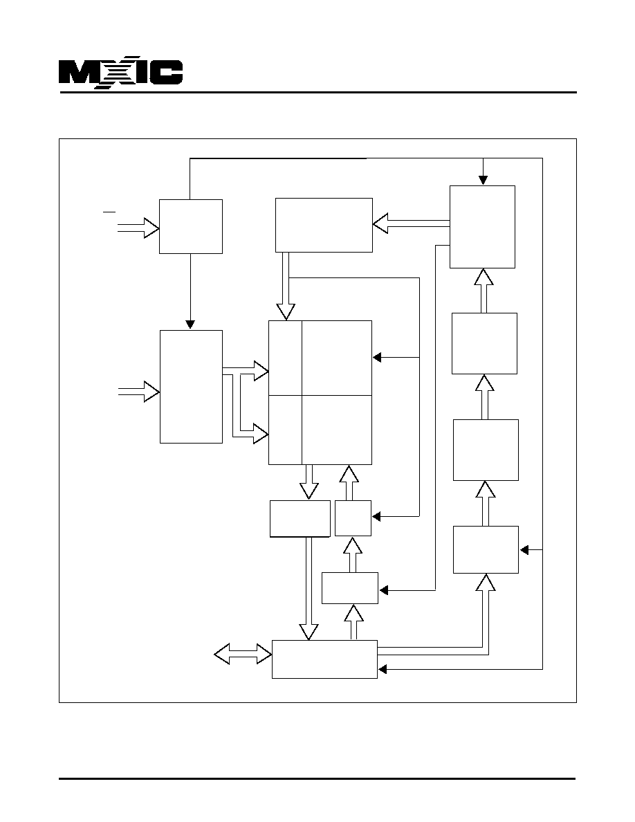
Register contents serve as inputs to an internal state-
machine which controls the erase and programming cir-
cuitry. During write cycles, the command register inter-
nally latches address and data needed for the program-
ming and erase operations. During a system write cycle,
addresses are latched on the falling edge of WE or CE,
whichever happens later, and data are latched on the
rising edge of WE or CE, whichever happens first.
MXIC's Flash technology combines years of EPROM
experience to produce the highest levels of quality, reli-
ability, and cost effectiveness. The MX29F004T/B elec-
trically erases all bits simultaneously using Fowler- tun-
neling. The bytes are programmed by using the EPROM
programming mechanism of hot electron injection.
During a program cycle, the state-machine will control
the program sequences and command register will not
respond to any command set. During a Sector Erase
cycle, the command register will only respond to Erase
Suspend command. After Erase Suspend is completed,
the device stays in read mode. After the state machine
has completed its task, it will allow the command regis-
ter to respond to its full command set.