3
P/N:PM0887
MX10E8050I /
Specifications subject to change without notice, contact your sales representatives for the most update information.
PRELIMINARY
MX10E8050IA
REV. 1.6, MAR. 28, 2005
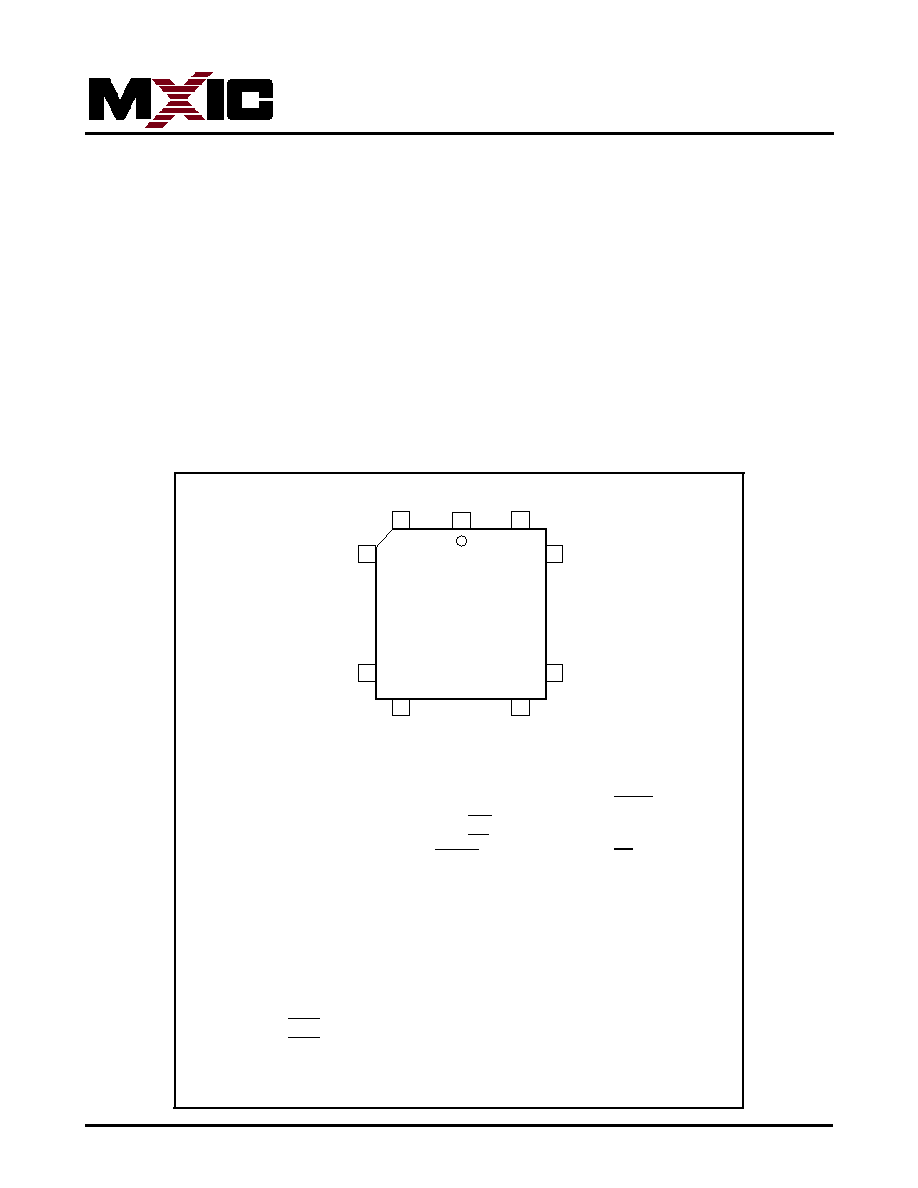
Package Type
PDIP
PLCC LQFP
I/O SYMBOL
PIN
PIN
PIN
DESCRIPTION
I/O P0.0-P0.7
39-32
43-36
37-30
Port:8-bit open drain bidirectional I/O Port
I/O P2.0-P2.7
21-28
24-31
18-25
Port: 8-bit quasi-bidirectional I/O Port with internal pull-up
I/O P1.0-P1.7
1-8
2-9
40-44,1-3
Port: 8-bit quasi-bidirectional I/O Port with internal pull-up
, except P1.6 and P1.7
I/O P3.0-P3.7
10-17
11,13-19
5,7-13
Port: 8-bit quasi-bidirectional I/O Port with internal pull-up
I/O P4.0~P4.3/
NA
23,34,1,12 17,28,39,6
4bit Quasi-bidirectional I/O port or PWM PWM0~PWM3
I
RESET
9
10
4
reset input
I
VCC
40
44
38
Positive power supply
I
VSS
20
22
16
Ground
I
XTAL1
19
21
15
XTAL connection input
O
XTAL2
18
20
14
XTAL connection output
O
PSEN
29
32
26
Program store enable output
O
ALE
30
33
27
Address latch enable output
I
EA
31
35
29
External access input
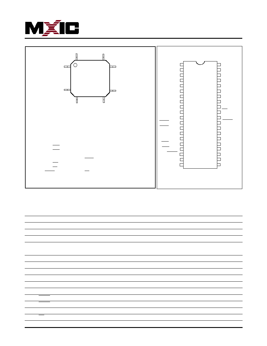
LQFP44
44
34
1
11
33
23
12
22
Pin
Function
1
P1.5
2
P1.6/SCL
3
P1.7/SDA
4
RST
5
P3.0/RxD
6 P4.3/PWM3
7
P3.1/TxD
8
P3.2/INT0
9
P3.3/INT1
10
P3.4/T0
11
P3.5/T1
12
P3.6/WR
13
P3.7/RD
14
XTAL2
15
XTAL1
Pin
Function
16
V
SS
17 P4.0/PWM0
18
P2.0/A8
19
P2.1/A9
20
P2.2/A10
21
P2.3/A11
22
P2.4/A12
23
P2.5/A13
24
P2.6/A14
25
P2.7/A15
26
PSEN
27
ALE
28 P4.1/PWM1
29
EA
30
P0.7/AD7
Pin
Function
31
P0.6/AD6
32
P0.5/AD5
33
P0.4/AD4
34
P0.3/AD3
35
P0.2/AD2
36
P0.1/AD1
37
P0.0/AD0
38
V
CC
39 P4.2/PWM2
40
P1.0/T2
41
P1.1/T2EX
42
P1.2
43
P1.3
44
P1.4
PDIP 40
1
2
3
4
5
6
7
8
9
10
11
12
13
14
15
16
17
18
19
20
(T2) P1.0
(T2EX) P1.1
P1.2
P1.3
P1.4
P1.5
(SCL)P1.6
(SDA)P1.7
RESET
(RXD) P3.0
(TXD)P3.1
(INT0) P3.2
(INT1) P3.3
(T0) P3.4
(T1) P3.5
(WR) P3.6
(RD) P3.7
XTAL2
XTAL1
VSS
40
39
38
37
36
35
34
33
32
31
30
29
28
27
26
25
24
23
22
21
VCC
P0.0 (AD0)
P0.1 (AD1)
P0.2 (AD2)
P0.3 (AD3)
P0.4 (AD4)
P0.5 (AD5)
P0.6 (AD6)
P0.7 (AD7)
EA
ALE
PSEN
P2.7 (A15)
P2.6 (A14)
P2.5 (A13)
P2.4 (A12)
P2.3 (A11)
P2.2 (A10)
P2.1 (A9)
P2.0 (A8)
Table. 1 Pin Description

4
P/N:PM0887
MX10E8050I /
Specifications subject to change without notice, contact your sales representatives for the most update information.
PRELIMINARY
MX10E8050IA
REV. 1.6, MAR. 28, 2005
Mnemonic
Pin Number
Type
Name and Function
PDIP
PLCC
LQFP
V
ss
20
22
16
I
Ground: 0 volt reference
V
cc
40
44
38
I
Power Supply: This is the power supply voltage for normal,
idle and power-down operation
P0.0 ~ 0.7
39-32
43-36
37-30
I/O
Port 0: Port 0 is an open drain, bi-directional I/O port. Port 0
pins have 1s written to them float and can be used as high
impedance inputs. Port 0 is also the multiplexed low-order
address and data bus during accessed to external program
and data memory. In this application, it uses strong internal
pull-ups when emitting 1s.
P1.0~1.7
1-8
2-9
40-44
I/O
Port1: Port 1 is an 8-bit bi-directional I/O port with internal
1-3
pull-ups. Port 1 pins that have 1s written to them are pulled
high by the internal pull-ups and can be used as inputs. As
inputs, Port 1 pins that are externally pulled low will source
current because of the internal pull-ups. Note that P1.6 and
P1.7 are open drain pins for I
2
C function.
Alternate functions for port 1 include:
1
2
40
I/O
T2(P1.0): Timer/Counter 2 external count input/clock out
2
3
41
I
T2EX(P1.1): Timer/Counter 2 Reload / Capture / Direction
control
3
4
42
I
SDA (P1.7): Data line for I
2
C
4
5
43
I/O
SCL (P1.6): Clock line for I
2
C
5
6
44
I/O
6
7
1
I/O
7
8
2
I/O
8
9
3
I/O
P2.0~2.7
21-28
24-31
18-25
I/O
Port 2 : Port 2 is an 8-bit bi-directional I/O port with internal
pull-ups. Port2 pins that have 1s written to them are pulled
high by the internal pull-ups and can be used as inputs. As
inputs, Port 2 pins that are externally pulled low will source
current because of the internal pull-ups. Port 2 emits the high
ordered address byte during fetches from external program
memory and during accesses to external data memory that
use 16-bit addresses (MOVX @DPTR). In this application, it
uses strong internal pull-ups when emitting 1s. During
accesses to external data memory using 8-bit addresses
(MOVX@R
I
), port 2 emits the contents of P2 special
`function register.
P3.0~3.7
10-17
11,
5,
I/O
Port 3: Port 3 is an 8-bit bi-directional I/O port with internal

5
P/N:PM0887
MX10E8050I /
Specifications subject to change without notice, contact your sales representatives for the most update information.
PRELIMINARY
MX10E8050IA
REV. 1.6, MAR. 28, 2005
13-19
7-13
pull-ups. Port 3 pins that have 1s written to them are pulled
high with the internal pull-ups and can be used as inputs. As
inputs, Port 3 pins that are externally pulled low will source
current because of the internal pull-ups. Port 3 also serves
the special features of MX10E8050I family, as listed below:
10
11
5
I
RxD (P3.0) : Serial input port
11
13
7
O
TxD (P3.1) : Serial output port
12
14
8
I
INT0 (P3.2) : External interrupt 0
13
15
9
I
INT1 (P3.3) : External interrupt 1
14
16
10
I
T0 (P3.4) : Timer 0 external input
15
17
11
I
T1 (P3.5) : Timer 1 external input
16
18
12
O
WR (P3.6) : External data memory write strobe
17
19
14
O
RD (P3.7) : External data memory read strobe
P4.0~P4.3
I/O
Port 4: Port 4 is an 4-bit bi-directional I/O port with internal
pull-ups. Port 4 pins that have 1s written to them are pulled
high with the internal pull-ups and can be used as inputs. As
inputs, Port 4 pins that are externally pulled low will source
current because of the internal pull-ups. Port 4 also serves
the special features of MX10E8050I family, as listed below:
P4.0
23
17
I
PWM0 (P4.0) : PWM module output 0
P4.1
34
28
I
PWM1 (P4.1) : PWM module output 1
P4.2
1
39
I
PWM2 (P4.2) : PWM module output 2
P4.3
12
6
I
PWM3 (P4.3) : PWM module output 3
RST
9
10
4
I
Reset : A high on this pin for eight machine cycles while the
oscillator is running, reset the devices.
ALE
30
33
27
O
Address Latch Enable: Output pulse for latching the low byte
of the address during an access to external memory. In
normal operation, ALE is emitted at constant rate of 1/6 the
oscillator frequency in 12x clock mode. 1/3 the oscillator
frequency in 6x clock mode, and can be used for external
timing or clocking. Note that one ALE pulse is skipped during
each access to external data memory.
PSEN
29
32
26
O
Program Strobe Enable: The read strobe to external program
memory. When executing code from external program
memory, PSEN is activated twice each machine cycle.,
except the two PSEN activation are skipped during each
access to external data memory. PSEN is not activated
during fetch from internal program memory.
EA
31
35
15
I
External Access Enable/ Programming Supply Voltage: EA
must be external held low to enable the device to fetch code
from external program memory locations 0000H and FFFFH
for 64 K devices.
XTAL 1
19
21
15
I
Crystal 1: Input to the inverting oscillator amplifier and input
to the internal clock generator circuits.
XTAL 2
18
20
14
O
Crystal 2: Output from the inverting oscillator amplifier.