
REV. 1.1, SEP. 30, 2005
1
P/N: PM1236
MX25L4005
4M-BIT [x 1] CMOS SERIAL FLASH
FEATURES
GENERAL
∑ Serial Peripheral Interface (SPI) compatible -- Mode 0
and Mode 3
∑ 4,194,304 x 1 bit structure
∑ 128 Equal Sectors with 4K byte each
- Any Sector can be erased individually
∑ 8 Equal Blocks with 64K byte each
- Any Block can be erased individually
∑ Single Power Supply Operation
- 2.7 to 3.6 volt for read, erase, and program operations
∑ Latch-up protected to 100mA from -1V to Vcc +1V
∑ Low Vcc write inhibit is from 1.5V to 2.5V
PERFORMANCE
∑ High Performance
- Fast access time: 70MHz serial clock (15pF + 1TTL
Load) and 66MHz serial clock (30pF + 1TTL Load)
- Fast program time: 1.4ms(typ.) and 5ms(max.)/page
(256-byte per page)
- Fast erase time: 60ms(typ.) and 120ms(max.)/sector
(4K-byte per sector) ; 1s(typ.) and 2s(max.)/block (64K-
byte per block)
∑ Low Power Consumption
- Low active read current: 12mA(max.) at 70MHz,
8mA(max.) at 66MHz and 4mA(max.) at 33MHz
- Low active programming current: 15mA (max.)
- Low active erase current: 15mA (max.)
- Low standby current: 10uA (max.)
- Deep power-down mode 1uA (typical)
∑ Minimum 100,000 erase/program cycles
SOFTWARE FEATURES
∑ Input Data Format
- 1-byte Command code
∑ Block Lock protection
- The BP0~BP2 status bit defines the size of the area
to be software protected against Program and Erase
instructions.
∑ Auto Erase and Auto Program Algorithm
-
Automatically erases and verifies data at selected
sector
-
Automatically programs and verifies data at selected
page by an internal algorithm that automatically times
the program pulse widths (Any page to be programed
should have page in the erased state first)
∑ Status Register Feature
∑ Electronic Identification
-
JEDEC 2-byte Device ID
- RES command, 1-byte Device ID
HARDWARE FEATURES
∑ SCLK Input
-
Serial clock input
∑ SI Input
-
Serial Data Input
∑ SO Output
-
Serial Data Output
∑ WP# pin
-
Hardware write protection
∑ HOLD# pin
-
pause the chip without diselecting the chip
∑ PACKAGE
-
8-pin SOP (150mil)
-
8-pin SOP (200mil)
- 8-land SON (6x5mm)
- All Pb-free devices are RoHS Compliant

2
P/N: PM1236
REV. 1.1, SEP. 30, 2005
MX25L4005
PIN CONFIGURATIONS
SYMBOL
DESCRIPTION
CS#
Chip Select
SI
Serial Data Input
SO
Serial Data Output
SCLK
Clock Input
HOLD#
Hold, to pause the device without
deselecting the device
WP#
Write Protection
VCC
+ 3.3V Power Supply
GND
Ground
PIN DESCRIPTION
GENERAL DESCRIPTION
The MX25L4005 is a CMOS 4,194,304 bit serial Flash
memory, which is configured as 524,288 x 8 internally. The
MX25L4005 feature a serial peripheral interface and soft-
ware protocol allowing operation on a simple 3-wire bus.
The three bus signals are a clock input (SCLK), a serial
data input (SI), and a serial data output (SO). SPI access
to the device is enabled by CS# input.
The MX25L4005 provide sequential read operation on
whole chip.
After program/erase command is issued, auto program/
erase algorithms which program/ erase and verify the
specified page or byte /sector/block locations will be
executed. Program command is executed on page (256
bytes) basis, and erase command is executes on chip or
sector(4K-bytes) or block(64K-bytes).
To provide user with ease of interface, a status register is
included to indicate the status of the chip. The status read
command can be issued to detect completion status of a
program or erase operation via WIP bit.
When the device is not in operation and CS# is high, it is
put in standby mode and draws less than 10uA DC current.
The MX25L4005 utilize MXIC's proprietary memory cell,
which reliably stores memory contents even after 100,000
program and erase cycles.
8-PIN SOP (150/200mil)
8-LAND SON (6x5mm)
1
2
3
4
CS#
SO
WP#
GND
8
7
6
5
VCC
HOLD#
SCLK
SI
1
2
3
4
CS#
SO
WP#
GND
VCC
HOLD#
SCLK
SI
8
7
6
5
3
P/N: PM1236
REV. 1.1, SEP. 30, 2005
MX25L4005
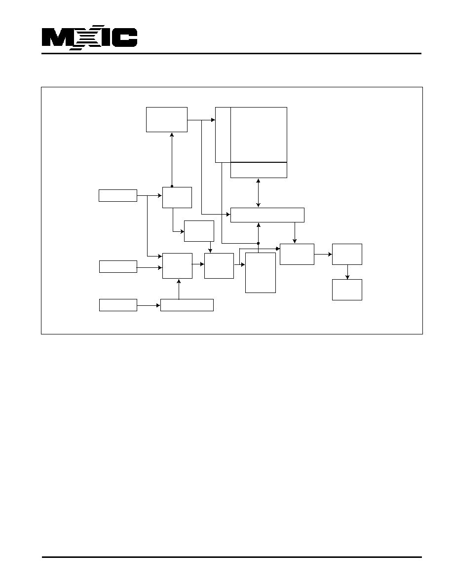
BLOCK DIAGRAM
Address
Generator
Memory Array
Page Buffer
Y-Decoder
X-Decoder
Data
Register
SRAM
Buffer
SI
SCLK
Clock Generator
State
Machine
Mode
Logic
Sense
Amplifier
HV
Generator
Output
Buffer
SO
CS#

4
P/N: PM1236
REV. 1.1, SEP. 30, 2005
MX25L4005
DATA PROTECTION
The MX25L4005 is designed to offer protection against
accidental erasure or programming caused by spurious
system level signals that may exist during power
transition. During power up the device automatically resets
the state machine in the Read mode. In addition, with its
control register architecture, alteration of the memory
contents only occurs after successful completion of
specific command sequences. The device also
incorporates several features to prevent inadvertent write
cycles resulting from VCC power-up and power-down
transition or system noise.
∑ Power-On Reset and an internal timer (tPUW) can
provide protection against inadvertant changes while
the power supply is outside the operating specification.
∑
Program, Erase and Write Status Register instructions
are checked that they consist of a number of clock
pulses that is a multiple of eight, before they are
accepted for execution.
∑ All instructions that modify data must be preceded by
a Write Enable (WREN) instruction to set the Write
Enable Latch (WEL) bit . This bit is returned to its reset
state by the following events:
- Power-up
- Write Disable (WRDI) instruction completion
- Write Status Register (WRSR) instruction completion
- Page Program (PP) instruction completion
- Sector Erase (SE) instruction completion
- Block Erase (BE) instruction completion
- Chip Erase (CE) instruction completion
∑
The Block Protect (BP2, BP1, BP0) bits allow part of
the memory to be configured as readonly. This is the
Software Protected Mode (SPM).
∑
The Write Protect (WP#) signal allows the Block
Protect (BP2, BP1, BP0) bits and Status Register
Write Disable (SRWD) bit to be protected. This is the
Hardware Protected Mode (HPM).
∑
In addition to the low power consumption feature, the
Deep Power-down mode offers extra software protec-
tion from inadvertent Write, Program and Erase in-
structions, as all instructions are ignored except one
particular instruction (the Release from Deep
Powerdown instruction).
∑ To avoid unexpected changes by system power supply
transition, the Power-On Reset and an internal timer
(tPUW) can protect the device.
∑ Before the Program, Erase, and Write Status Register
execution, instruction length will be checked on follow-
ing the clock pulse number to be multiple of eight base.
∑ Write Enable (WREN) instruction must set to Write
Enable Latch (WEL) bit before writing other instructions
to modify data. The WEL bit will return to reset state by
following situations:
- Power-up
- Write Disable (WRDI) instruction completion
- Write Status Register (WRSR) instruction completion
- Page Program (PP) instruction completion
- Sector Erase (SE) instruction completion
- Block Erase (BE) instruction completion
- Chip Erase (CE) instruction completion
∑ The Software Protected Mode (SPM) use (BP2, BP1,
BP0) bits to allow part of memory to be protected as
read only.
∑ The Hardware Protected Mode (HPM) use WP# to
protect the (BP2, BP1, BP0) bits and SRWD bit.
∑ Deep-Power Down Mode also protects the device by
ignoring all instructions except Release from Deep-
Power Down (RDP) instruction and RES instruction.

5
P/N: PM1236
REV. 1.1, SEP. 30, 2005
MX25L4005
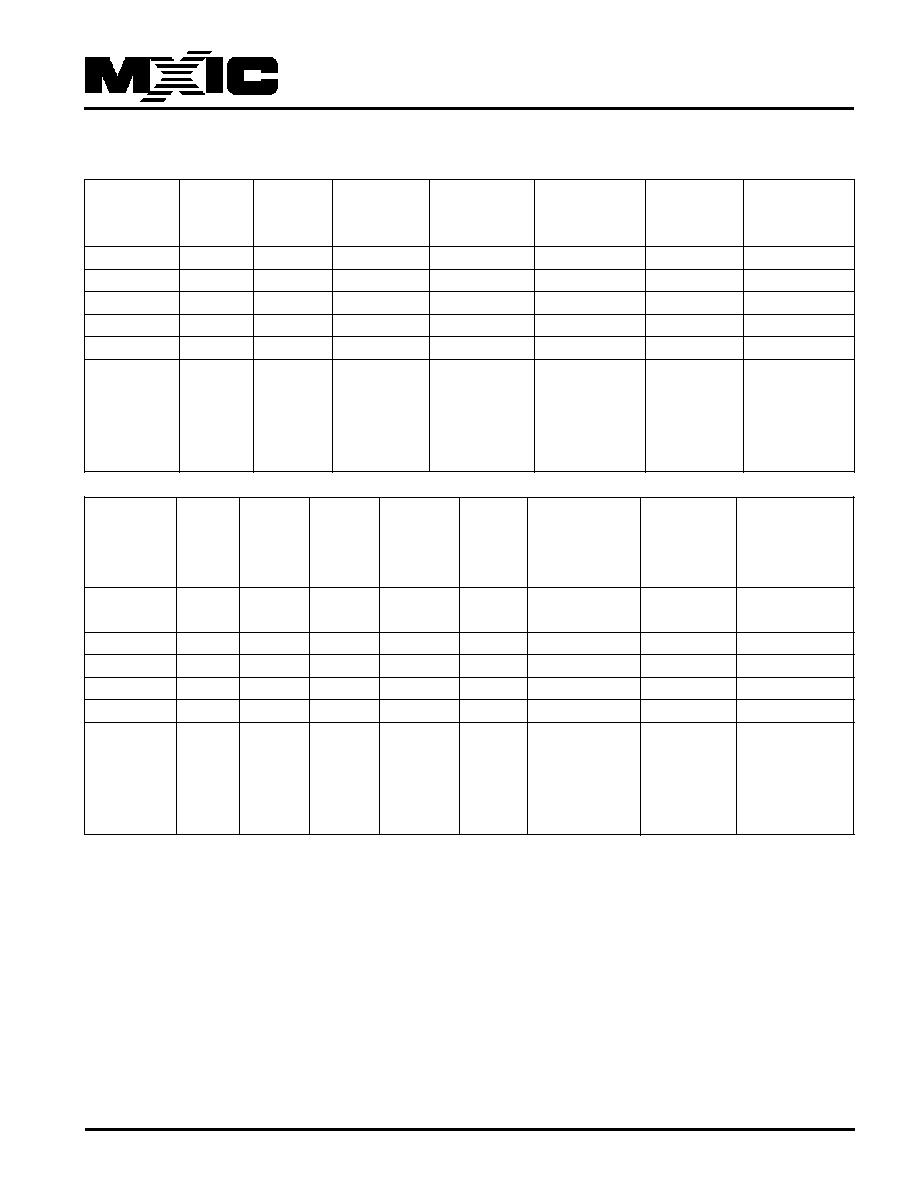
Table 1. Protected Area Sizes
Status bit
Protect level
4Mb
BP2
BP1
BP0
0
0
0
0 (none)
None
0
0
1
1 (1 block)
Block 7
0
1
0
2 (2 blocks)
Block 6-7
0
1
1
3 (4 blocks)
Block 4-7
1
0
0
4 (8 blocks)
All
1
0
1
5 (All)
All
1
1
0
6 (All)
All
1
1
1
7 (All)
All

6
P/N: PM1236
REV. 1.1, SEP. 30, 2005
MX25L4005
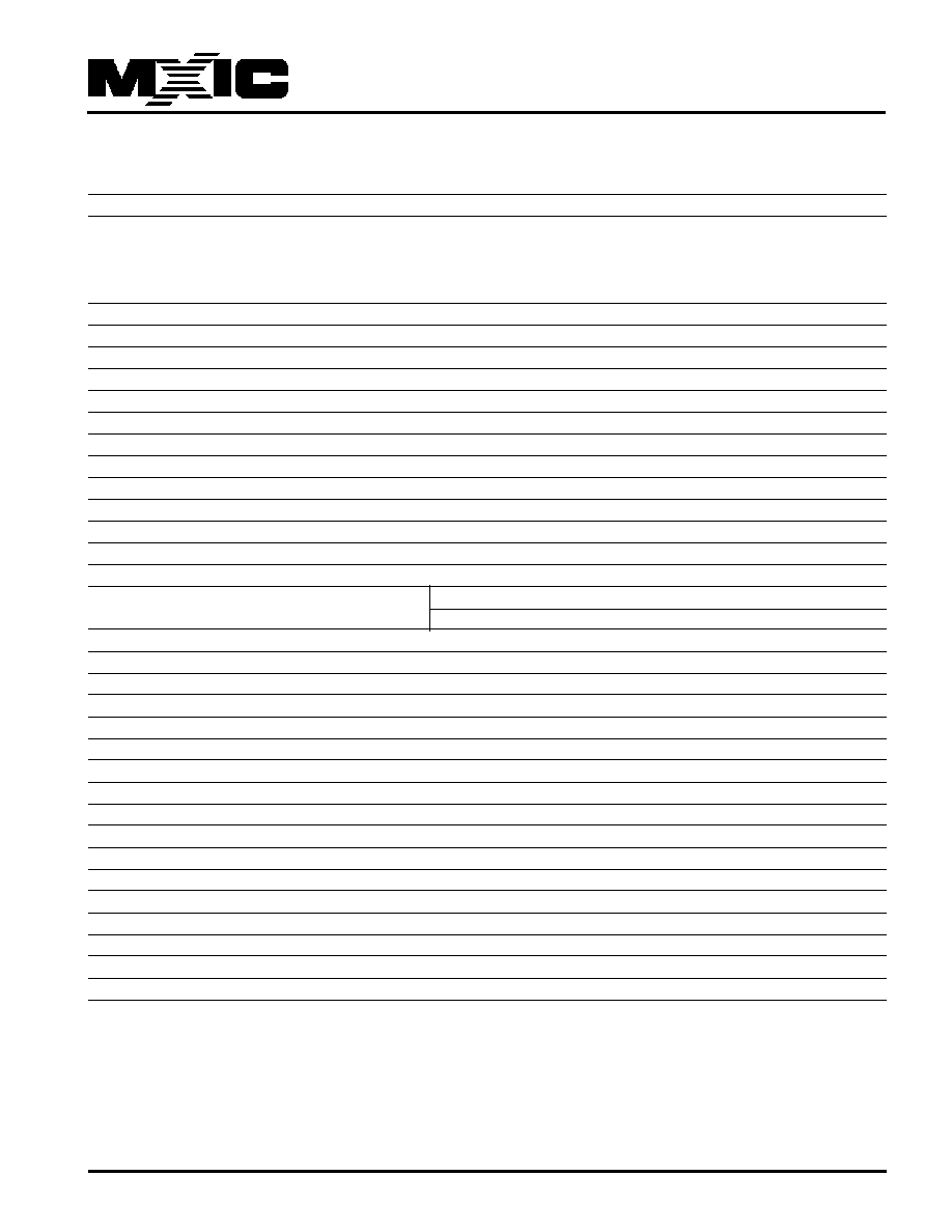
HOLD FEATURE
HOLD# pin signal goes low to hold any serial communications with the device. The HOLD feature will not stop the operation
of write status register, programming, or erasing in progress.
The operation of HOLD requires Chip Select(CS#) keeping low and starts on falling edge of HOLD# pin signal while Serial
Clock (SCLK) signal is being low (if Serial Clock signal is not being low, HOLD operation will not start until Serial Clock
signal being low). The HOLD condition ends on the rising edge of HOLD# pin signal while Serial Clock(SCLK) signal is
being low( if Serial Clock signal is not being low, HOLD operation will not end until Serial Clock being low), see Figure 1.
Figure 1. Hold Condition Operation
The Serial Data Output (SO) is high impedance, both Serial Data Input (SI) and Serial Clock (SCLK) are don't care during
the HOLD operation. If Chip Select (CS#) signal goes high during HOLD operation, it has the effect on resetting the internal
logic of the device. It is necessary to drive HOLD# signal to high, and then to drive CS# to low for restarting communication
with the device.
HOLD#
SCLK
Hold
Condition
(standard use)
Hold
Condition
(non-standard use)
7
P/N: PM1236
REV. 1.1, SEP. 30, 2005
MX25L4005
Table 2. COMMAND DEFINITION
COMMAND WREN
WRDI
RDID
RDSR
WRSR
READ
Fast Read
(byte)
(write
(write
(read ident-
(read status
(write status
(read data)
(fast read
Enable)
disable)
ification)
register)
register)
data)
1st
06 Hex
04 Hex
9F Hex
05 Hex
01 Hex
03 Hex
0B Hex
2nd
AD1
AD1
3rd
AD2
AD2
4th
AD3
AD3
5th
x
Action
sets the
reset the
output the
to read out
to write new
n bytes
(WEL)
(WEL)
manufacturer the status
values to the
read out
write
write
ID and 2-byte register
status register until
enable
enable
device ID
CS# goes
latch bit
latch bit
high
COMMAND SE
BE
CE
PP
DP
RDP
RES
REMS (Read
(byte)
(Sector
(Block
(Chip
(Page
(Deep
(Release
(Read
Electronic
Erase)
Erase)
Erase)
Program)
Power
from Deep
Electronic
Manufacturer
Down)
Power-down)
ID)
& Device ID)
1st
20 Hex
52 or
60 or
02 Hex
B9 Hex
AB Hex
AB Hex
90 Hex
D8 Hex
C7 Hex
2nd
AD1
AD1
AD1
x
x
3rd
AD2
AD2
AD2
x
x
4th
AD3
AD3
AD3
x
ADD(1)
5th
Action
Output the
manufacturer
ID and device
ID
(1) ADD=00H will output the manufacturer's ID first and ADD=01H will output device ID first

8
P/N: PM1236
REV. 1.1, SEP. 30, 2005
MX25L4005
Table 3. Memory Organization
Block
Sector
127
07F000h
07FFFFh
......
..
......
.
......
..
112
070000h
070FFFh
111
06F000h
06FFFFh
......
..
......
.
......
..
96
060000h
060FFFh
95
05F000h
05FFFFh
......
..
......
.
......
..
80
050000h
050FFFh
79
04F000h
04FFFFh
......
..
......
.
......
..
64
040000h
040FFFh
63
03F000h
03FFFFh
......
..
......
.
......
..
48
030000h
030FFFh
47
02F000h
02FFFFh
......
..
......
.
......
..
32
020000h
020FFFh
31
01F000h
01FFFFh
......
..
......
.
......
..
16
010000h
010FFFh
15
00F000h
00FFFFh
......
..
......
.
......
..
3
003000h
003FFFh
2
002000h
002FFFh
001000h
001FFFh
000000h
000FFFh
1
0
Address Range
7
6
5
4
3
2
1
0

9
P/N: PM1236
REV. 1.1, SEP. 30, 2005
MX25L4005
DEVICE OPERATION
1. Before a command is issued, status register should be checked to ensure device is ready for the intended operation.
2. When incorrect command is inputted to this LSI, this LSI becomes standby mode and keeps the standby mode until
next CS# falling edge. In standby mode, SO pin of this LSI should be High-Z.
3. When correct command is inputted to this LSI, this LSI becomes active mode and keeps the active mode until next
CS# rising edge.
4. Input data is latched on the rising edge of Serial Clock(SCLK) and data shifts out on the falling edge of SCLK. The
difference of SPI mode 0 and mode 3 is shown as Figure 2.
Figure 2.
SPI Modes Supported
5. For the following instructions: RDID, RDSR, READ, FAST_READ, RES and REMS the shifted-in instruction sequence
is followed by a data-out sequence. After any bit of data being shifted out, the CS# can be high. For the following
instructions: WREN, WRDI, WRSR, SE, BE, CE, PP, RDP and DP the CS# must go high exactly at the byte boundary;
otherwise, the instruction will be rejected and not executed.
6. During the progress of Write Status Register, Program, Erase operation, to access the memory array is neglected and
not affect the current operation of Write Status Register, Program, Erase.
SCLK
MSB
CPHA
SI
0
1
CPOL
0
(SPI mode 0)
(SPI mode 3)
1
SO
SCLK
MSB

10
P/N: PM1236
REV. 1.1, SEP. 30, 2005
MX25L4005
COMMAND DESCRIPTION
(1) Write Enable (WREN)
The Write Enable (WREN) instruction is for setting Write Enable Latch (WEL) bit. For those instructions like PP, SE, BE,
CE, and WRSR, which are intended to change the device content, should be set every time after the WREN instruction
setting the WEL bit.
The sequence of issuing WREN instruction is: CS# goes low-> sending WREN instruction code-> CS# goes high. (see
Figure 11)
(2) Write Disable (WRDI)
The Write Disable (WRDI) instruction is for resetting Write Enable Latch (WEL) bit.
The sequence of issuing WRDI instruction is: CS# goes low-> sending WRDI instruction code-> CS# goes high. (see Figure
12)
The WEL bit is reset by following situations:
- Power-up
- Write Disable (WRDI) instruction completion
- Write Status Register (WRSR) instruction completion
- Page Program (PP) instruction completion
- Sector Erase (SE) instruction completion
- Block Erase (BE) instruction completion
- Chip Erase (CE) instruction completion
(3) Read Identification (RDID)
The RDID instruction is for reading the manufacturer ID of 1-byte and followed by Device ID of 2-byte. The MXIC
Manufacturer ID is C2(hex), the memory type ID is 20(hex) as the first-byte device ID, and the individual device ID of
second-byte ID is as followings: 13(hex) for MX25L4005.
The sequence of issuing RDID instruction is: CS# goes low-> sending RDID instruction code -> 24-bits ID data out on SO
-> to end RDID operation can use CS# to high at any time during data out. (see Figure. 13)
While Program/Erase operation is in progress, it will not decode the RDID instruction, so there's no effect on the cycle of
program/erase operation which is currently in progress. When CS# goes high, the device is at standby stage.
11
P/N: PM1236
REV. 1.1, SEP. 30, 2005
MX25L4005
(4) Read Status Register (RDSR)
The RDSR instruction is for reading Status Register Bits. The Read Status Register can be read at any time (even in
program/erase/write status register condition) and continuously. It is recommended to check the Write in Progress (WIP)
bit before sending a new instruction when a program, erase, or write status register operation is in progress.
The sequence of issuing RDSR instruction is: CS# goes low-> sending RDSR instruction code-> Status Register data out
on SO (see Figure. 14)
The definition of the status register bits is as below:
WIP bit. The Write in Progress (WIP) bit, a volatile bit, indicates whether the device is busy in program/erase/write status
register progress. When WIP bit sets to 1, which means the device is busy in program/erase/write status register progress.
When WIP bit sets to 0, which means the device is not in progress of program/erase/write status register cycle.
WEL bit. The Write Enable Latch (WEL) bit, a volatile bit, indicates whether the device is set to internal write enable latch.
When WEL bit sets to 1, which means the internal write enable latch is set, the device can accept program/erase/write
status register instruction. When WEL bit sets to 0, which means no internal write enable latch; the device will not accept
program/erase/write status register instruction.
BP2, BP1, BP0 bits. The Block Protect (BP2, BP1, BP0) bits, non-volatile bits, indicate the protected area(as defined
in table 1) of the device to against the program/erase instruction without hardware protection mode being set. To write the
Block Protect (BP2, BP1, BP0) bits requires the Write Status Register (WRSR) instruction to be executed. Those bits
define the protected area of the memory to against Page Program (PP), Sector Erase (SE), Block Erase (BE) and Chip
Erase(CE) instructions (only if all Block Protect bits set to 0, the CE instruction can be executed)
SRWD bit. The Status Register Write Disable (SRWD) bit, non-volatile bit, is operated together with Write Protection (WP#)
pin for providing hardware protection mode. The hardware protection mode requires SRWD sets to 1 and WP# pin signal
is low stage. In the hardware protection mode, the Write Status Register (WRSR) instruction is no longer accepted for
execution and the SRWD bit and Block Protect bits (BP2, BP1, BP0) are read only.
bit 7
bit 6
bit 5
bit 4
bit 3
bit 2
bit 1
bit 0
SRWD
BP2
BP1
BP0
WEL
WIP
Status
0
0
the level of the level of the level of
(write enable
(write in progress
Register Write
protected
protected
protected
latch)
bit)
Protect
block
block
block
1= status
(note 1)
(note 1)
(note 1)
1=write enable 1=write operation
register write
0=not write
0=not in write
disable
enable
operation
Note: 1. see the table "Protected Area Sizes"

12
P/N: PM1236
REV. 1.1, SEP. 30, 2005
MX25L4005
(5) Write Status Register (WRSR)
The WRSR instruction is for changing the values of Status Register Bits. Before sending WRSR instruction, the Write
Enable (WREN) instruction must be decoded and executed to set the Write Enable Latch (WEL) bit in advance. The WRSR
instruction can change the value of Block Protect (BP2, BP1, BP0) bits to define the protected area of memory (as shown
in table 1). The WRSR also can set or reset the Status Register Write Disable (SRWD) bit in accordance with Write
Protection (WP#) pin signal. The WRSR instruction cannot be executed once the Hardware Protected Mode (HPM) is
entered.
The sequence of issuing WRSR instruction is: CS# goes low-> sending WRSR instruction code-> Status Register data
on SI-> CS# goes high. (see Figure 15)
The WRSR instruction has no effect on b6, b5, b1, b0 of the status register.
The CS# must go high exactly at the byte boundary; otherwise, the instruction will be rejected and not executed. The self-
timed Write Status Register cycle time (tW) is initiated as soon as Chip Select (CS#) goes high. The Write in Progress
(WIP) bit still can be check out during the Write Status Register cycle is in progress. The WIP sets 1 during the tW timing,
and sets 0 when Write Status Register Cycle is completed, and the Write Enable Latch (WEL) bit is reset.
Table 4. Protection Modes
Note:
1. As defined by the values in the Block Protect (BP2, BP1, BP0) bits of the Status Register, as shown in Table 1.
As the above table showing, the summary of the Software Protected Mode (SPM) and Hardware Protected Mode (HPM).
Software Protected Mode (SPM):
-
When SRWD bit=0, no matter WP# is low or high, the WREN instruction may set the WEL bit and can change the values
of SRWD, BP2, BP1, BP0. The protected area, which is defined by BP2, BP1, BP0, is at software protected mode
(SPM).
-
When SRWD bit=1 and WP# is high, the WREN instruction may set the WEL bit can change the values of SRWD, BP2,
BP1, BP0. The protected area, which is defined by BP2, BP1, BP0, is at software protected mode (SPM)
WP#
Signal
SRWD
Bit
Mode
Write Protection of the
Status Register
Memory Content
Protected Area
1
Unprotected Area
1
1
0
Software
Protected
(SPM)
Status Register is
Writable (if the WREN
instruction has set the
WEL bit)
The values in the SRWD,
BP2, BP1 and BP0
bits can be changed
Protected against Page
Program, Sector Erase
and Chip Erase
Ready to accept Page
Program and Sector
Erase instructions
0
0
1
1
0
1
Hardware
Protected
(HPM)
Status Register is
Hardware write protected
The values in the SRWD,
BP2, BP1 and BP0
bits cannot be changed
Protected against Page
Program, Sector Erase
and Chip Erase
Ready to accept Page
Program and Sector
Erase instructions

13
P/N: PM1236
REV. 1.1, SEP. 30, 2005
MX25L4005
Note: If SRWD bit=1 but WP# is low, it is impossible to write the Status Register even if the WEL bit has previously been
set. It is rejected to write the Status Register and not be executed.
Hardware Protected Mode (HPM):
-
When SRWD bit=1, and then WP# is low (or WP# is low before SRWD bit=1), it enters the hardware protected mode
(HPM). The data of the protected area is protected by software protected mode by BP2, BP1, BP0 and hardware
protected mode by the WP# to against data modification.
Note: to exit the hardware protected mode requires WP# driving high once the hardware protected mode is entered. If the
WP# pin is permanently connected to high, the hardware protected mode can never be entered; only can use software
protected mode via BP2, BP1, BP0.
(6) Read Data Bytes (READ)
The read instruction is for reading data out. The address is latched on rising edge of SCLK, and data shifts out on the falling
edge of SCLK at a maximum frequency fR. The first address byte can be at any location. The address is automatically
increased to the next higher address after each byte data is shifted out, so the whole memory can be read out at a single
READ instruction. The address counter rolls over to 0 when the highest address has been reached.
The sequence of issuing READ instruction is: CS# goes low-> sending READ instruction code-> 3-byte address on SI
-> data out on SO-> to end READ operation can use CS# to high at any time during data out. (see Figure. 16)
(7) Read Data Bytes at Higher Speed (FAST_READ)
The FAST_READ instruction is for quickly reading data out. The address is latched on rising edge of SCLK, and data of
each bit shifts out on the falling edge of SCLK at a maximum frequency fC. The first address byte can be at any location.
The address is automatically increased to the next higher address after each byte data is shifted out, so the whole memory
can be read out at a single FAST_READ instruction. The address counter rolls over to 0 when the highest address has
been reached.
The sequence of issuing FAST_READ instruction is: CS# goes low-> sending FAST_READ instruction code-> 3-byte
address on SI-> 1-dummy byte address on SI->data out on SO-> to end FAST_READ operation can use CS# to high at
any time during data out. (see Figure. 17)
While Program/Erase/Write Status Register cycle is in progress, FAST_READ instruction is rejected without any impact
on the Program/Erase/Write Status Register current cycle.
(8) Sector Erase (SE)
The Sector Erase (SE) instruction is for erasing the data of the chosen sector to be "1". A Write Enable (WREN) instruction
must execute to set the Write Enable Latch (WEL) bit before sending the Sector Erase (SE). Any address of the sector
(see table 3) is a valid address for Sector Erase (SE) instruction. The CS# must go high exactly at the byte boundary (the
latest eighth of address byte been latched-in); otherwise, the instruction will be rejected and not executed.
Address bits [Am-A12] (Am is the most significant address) select the sector address.
The sequence of issuing SE instruction is: CS# goes low -> sending SE instruction code-> 3-byte address on SI -> CS#
goes high. (see Figure 19)

14
P/N: PM1236
REV. 1.1, SEP. 30, 2005
MX25L4005
The self-timed Sector Erase Cycle time (tSE) is initiated as soon as Chip Select (CS#) goes high. The Write in Progress
(WIP) bit still can be check out during the Sector Erase cycle is in progress. The WIP sets 1 during the tSE timing, and
sets 0 when Sector Erase Cycle is completed, and the Write Enable Latch (WEL) bit is reset. If the page is protected by
BP2, BP1, BP0 bits, the Sector Erase (SE) instruction will not be executed on the page.
(9) Block Erase (BE)
The Block Erase (BE) instruction is for erasing the data of the chosen block to be "1". A Write Enable (WREN) instruction
must execute to set the Write Enable Latch (WEL) bit before sending the Block Erase (BE). Any address of the block
(see table 3) is a valid address for Block Erase (BE) instruction. The CS# must go high exactly at the byte boundary (the
latest eighth of address byte been latched-in); otherwise, the instruction will be rejected and not executed.
The sequence of issuing BE instruction is: CS# goes low -> sending BE instruction code-> 3-byte address on SI -> CS#
goes high. (see Figure 20)
The self-timed Block Erase Cycle time (tBE) is initiated as soon as Chip Select (CS#) goes high. The Write in Progress
(WIP) bit still can be check out during the Sector Erase cycle is in progress. The WIP sets 1 during the tBE timing, and
sets 0 when Sector Erase Cycle is completed, and the Write Enable Latch (WEL) bit is reset. If the page is protected by
BP2, BP1, BP0 bits, the Block Erase (BE) instruction will not be executed on the page.
(10) Chip Erase (CE)
The Chip Erase (CE) instruction is for erasing the data of the whole chip to be "1". A Write Enable (WREN) instruction must
execute to set the Write Enable Latch (WEL) bit before sending the Chip Erase (CE). Any address of the sector (see table
3) is a valid address for Chip Erase (CE) instruction. The CS# must go high exactly at the byte boundary( the latest eighth
of address byte been latched-in); otherwise, the instruction will be rejected and not executed.
The sequence of issuing CE instruction is: CS# goes low-> sending CE instruction code-> CS# goes high. (see Figure
20)
The self-timed Chip Erase Cycle time (tCE) is initiated as soon as Chip Select (CS#) goes high. The Write in Progress
(WIP) bit still can be check out during the Chip Erase cycle is in progress. The WIP sets 1 during the tCE timing, and
sets 0 when Chip Erase Cycle is completed, and the Write Enable Latch (WEL) bit is reset. If the chip is protected by BP2,
BP1, BP0 bits, the Chip Erase (CE) instruction will not be executed. It will be only executed when BP2, BP1, BP0 all set
to "0".
(11) Page Program (PP)
The Page Program (PP) instruction is for programming the memory to be "0". A Write Enable (WREN) instruction must
execute to set the Write Enable Latch (WEL) bit before sending the Page Program (PP). If the eight least significant
address bits (A7-A0) are not all 0, all transmitted data which goes beyond the end of the current page are programmed
from the start address if the same page (from the address whose 8 least significant address bits (A7-A0) are all 0). The
CS# must keep during the whole Page Program cycle. The CS# must go high exactly at the byte boundary( the latest
eighth of address byte been latched-in); otherwise, the instruction will be rejected and not executed. If more than 256 bytes
are sent to the device, the data of the last 256-byte is programmed at the request page and previous data will be
disregarded. If less than 256 bytes are sent to the device, the data is programmed at the request address of the page
without effect on other address of the same page.
The sequence of issuing PP instruction is: CS# goes low-> sending PP instruction code-> 3-byte address on SI-> at least
1-byte on data on SI-> CS# goes high. (see Figure 18)

15
P/N: PM1236
REV. 1.1, SEP. 30, 2005
MX25L4005
(12) Deep Power-down (DP)
The Deep Power-down (DP) instruction is for setting the device on the minimizing the power consumption (to entering the
Deep Power-down mode), the standby current is reduced from ISB1 to ISB2). The Deep Power-down mode requires the
Deep Power-down (DP) instruction to enter, during the Deep Power-down mode, the device is not active and all Write/
Program/Erase instruction are ignored. When CS# goes high, it's only in standby mode not deep power-down mode. It's
different from Standby mode.
The sequence of issuing DP instruction is: CS# goes low-> sending DP instruction code-> CS# goes high. (see Figure 22)
Once the DP instruction is set, all instruction will be ignored except the Release from Deep Power-down mode (RDP) and
Read Electronic Signature (RES) instruction. (RES instruction to allow the ID been read out). When Power-down, the deep
power-down mode automatically stops, and when power-up, the device automatically is in standby mode. For RDP
instruction the CS# must go high exactly at the byte boundary (the latest eighth bit of instruction code been latched-in);
otherwise, the instruction will not executed. As soon as Chip Select (CS#) goes high, a delay of tDP is required before
entering the Deep Power-down mode and reducing the current to ISB2.
(13) Release from Deep Power-down (RDP), Read Electronic Signature (RES)
The Release from Deep Power-down (RDP) instruction is terminated by driving Chip Select (CS#) High. When Chip Select
(CS#) is driven High, the device is put in the Stand-by Power mode. If the device was not previously in the Deep Power-
down mode, the transition to the Stand-by Power mode is immediate. If the device was previously in the Deep Power-down
mode, though, the transition to the Stand-by Power mode is delayed by tRES2, and Chip Select (CS#) must remain High
for at least tRES2(max), as specified in Table 6. Once in the Stand-by Power mode, the device waits to be selected, so
that it can receive, decode and execute instructions.
RES instruction is for reading out the old style of 8-bit Electronic Signature, whose values are shown as table of ID
Definitions. This is not the same as RDID instruction. It is not recommended to use for new design. For new deisng, please
use RDID instruction. Even in Deep power-down mode, the RDP and RES are also allowed to be executed, only except
the device is in progress of program/erase/write cycle; there's no effect on the current program/erase/write cycle in
progress.
The sequence is shown as Figure 23,24.
The RES instruction is ended by CS# goes high after the ID been read out at least once. The ID outputs repeatedly if
continuously send the additional clock cycles on SCLK while CS# is at low. If the device was not previously in Deep Power-
down mode, the device transition to standby mode is immediate. If the device was previously in Deep Power-down mode,
there's a delay of tRES2 to transit to standby mode, and CS# must remain to high at least tRES2(max). Once in the standby
mode, the device waits to be selected, so it can be receive, decode, and execute instruction.
The RDP instruction is for releasing from Deep Power Down Mode.
The self-timed Page Program Cycle time (tPP) is initiated as soon as Chip Select (CS#) goes high. The Write in Progress
(WIP) bit still can be check out during the Page Program cycle is in progress. The WIP sets 1 during the tPP timing, and
sets 0 when Page Program Cycle is completed, and the Write Enable Latch (WEL) bit is reset. If the page is protected by
BP2, BP1, BP0 bits, the Page Program (PP) instruction will not be executed.

16
P/N: PM1236
REV. 1.1, SEP. 30, 2005
MX25L4005
(14) Read Electronic Manufacturer ID & Device ID (REMS)
The REMS instruction is an alternative to the Release from Power-down/Device ID instruction that provides both the JEDEC
assigned manufacturer ID and the specific device ID.
The REMS instruction is very similar to the Release from Power-down/Device ID instruction. The instruction is initiated
by driving the CS# pin low and shift the instruction code "90h" followed by two dummy bytes and one bytes address (A7~A0).
After which, the Manufacturer ID for MXIC (C2h) and the Device ID are shifted out on the falling edge of SCLK with most
significant bit (MSB) first as shown in figure 25. The Device ID values are listed in Table of ID Definitions on page 16. If
the one-byte address is initially set to 01h, then the device ID will be read first
and then followed by the Manufacturer ID.
The Manufacturer and Device IDs can be read continuously, alternating from one to the other. The instruction is completed
by driving CS# high.
Table of ID Definitions:
RDID Command
manufacturer ID
memory type
memory density
C2
20
13
RES Command
electronic ID
12
REMS Command
manufacturer ID
device ID
C2
12

17
P/N: PM1236
REV. 1.1, SEP. 30, 2005
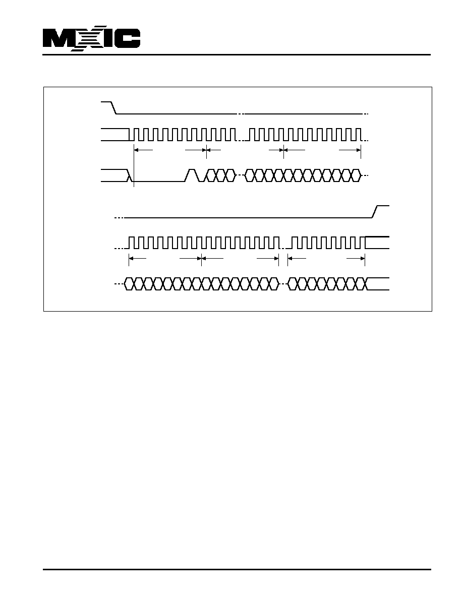
MX25L4005
POWER-ON STATE
At Power-up and Power-down, the device must not be selected (that is Chip Select (CS#) must follow the voltage applied
on V
CC
) until V
CC
reaches the correct value:
- V
CC
(min) at Power-up, and then for a further delay of t
VSL
- V
SS
at Power-down
Usually a simple pull-up resistor on Chip Select (CS#) can be used to insure safe and proper Power-up and Power-down.
To avoid data corruption and inadvertent write operations during power up, a Power On Reset (POR) circuit is included. The
logic inside the device is held reset while V
CC
is less than the POR threshold value, V
WI
--all operations are disabled, and
the device does not respond to any instruction.
Moreover, the device ignores all Write Enable (WREN), Page Program (PP), Sector Erase (SE), Block Erase (BE), Chip
Erase (CE) and Write Status Register (WRSR) instructions until a time delay of t
PUW
has elapsed after the moment that
V
CC
rises above the V
WI
threshold. However, the correct operation of the device is not guaranteed if, by this time, V
CC
is
still below V
CC
(min). No Write Status Register, Program or Erase instructions should be sent until the later of:
- t
PUW
after V
CC
passed the V
WI
threshold
- t
VSL
after V
CC
passed the V
CC
(min) level
These values are specified in Table 7.
If the delay, t
VSL
, has elapsed, after V
CC
has risen above V
CC
(min), the device can be selected for READ instructions even
if the t
PUW
delay is not yet fully elapsed.
At Power-up, the device is in the following state:
- The device is in the Standby mode (not the Deep Power-down mode).
- The Write Enable Latch (WEL) bit is reset.
Normal precautions must be taken for supply rail decoupling, to stabilize the V
CC
feed. Each device in a system should
have the V
CC
rail decoupled by a suitable capacitor close to the package pins. (Generally, this capacitor is of the order of
0.1uF).
At Power-down, when V
CC
drops from the operating voltage, to below the POR threshold value, V
WI
, all operations are
disabled and the device does not respond to any instruction. (The designer needs to be aware that if a Power-down occurs
while a Write, Program or Erase cycle is in progress, some data corruption can result.)

18
P/N: PM1236
REV. 1.1, SEP. 30, 2005
MX25L4005
NOTICE:
1. Stresses greater than those listed under ABSOLUTE
MAXIMUM RATINGS may cause permanent damage
to the device. This is stress rating only and functional
operational sections of this specification is not implied.
Exposure to absolute maximum rating conditions for
extended period may affect reliability.
2. Specifications contained within the following tables are
subject to change.
3. During voltage transitions, all pins may overshoot to
4.6V or -0.5V for period up to 20ns.
4. All input and output pins may overshoot to VCC+0.5V
while VCC+0.5V is smaller than or equal to 4.6V.
RATING
VALUE
Ambient Operating Temperature -40
∞
C to 85
∞
C for
Industrial grade
0
∞
C to 70
∞
C for
Commercial grade
Storage Temperature
-55
∞
C to 125
∞
C
Applied Input Voltage
-0.5V to 4.6V
Applied Output Voltage
-0.5V to 4.6V
VCC to Ground Potential
-0.5V to 4.6V
ABSOLUTE MAXIMUM RATINGS
ELECTRICAL SPECIFICATIONS
CAPACITANCE TA = 25
∞∞
∞∞
∞
C, f = 1.0 MHz
SYMBOL
PARAMETER
MIN.
TYP
MAX.
UNIT
CONDITIONS
CIN
Input Capacitance
6
pF
VIN = 0V
COUT
Output Capacitance
8
pF
VOUT = 0V
Figure 3.Maximum Negative Overshoot Waveform
0V
-0.5V
20ns
Figure 4. Maximum Positive Overshoot Waveform
4.6V
3.6V
20ns

19
P/N: PM1236
REV. 1.1, SEP. 30, 2005
MX25L4005
Figure 5. INPUT TEST WAVEFORMS AND MEASUREMENT LEVEL
Figure 6. OUTPUT LOADING
AC
Measurement
Level
Input timing referance level
Output timing referance level
0.8VCC
0.7VCC
0.3VCC
0.5VCC
0.2VCC
Note: Input pulse rise and fall time are <5ns
DEVICE UNDER
TEST
DIODES=IN3064
OR EQUIVALENT
CL
6.2K ohm
2.7K ohm
+3.3V
CL=30pF Including jig capacitance
(CL=15pF Including jig capacitance for 70MHz)
20
P/N: PM1236
REV. 1.1, SEP. 30, 2005
MX25L4005
SYMBOL PARAMETER
NOTES
MIN.
TYP
MAX.
UNITS
TEST CONDITIONS
ILI
Input Load
1
±
2
uA
VCC = VCC Max
Current
VIN = VCC or GND
ILO
Output Leakage
1
±
2
uA
VCC = VCC Max
Current
VIN = VCC or GND
ISB1
VCC Standby
1
10
uA
VIN = VCC or GND
Current
CS# = VCC
ISB2
Deep Power-down
10
uA
VIN = VCC or GND
Current
CS# = VCC
ICC1
VCC Read
1
12
mA
f=70MHz
SCLK=0.1VCC/0.9VCC, SO=Open
8
mA
f=66MHz
SCLK=0.1VCC/0.9VCC, SO=Open
4
mA
f=33MHz
SCLK=0.1VCC/0.9VCC, SO=Open
ICC2
VCC Program
1
15
mA
Program in Progress
Current (PP)
CS# = VCC
ICC3
VCC Write Status
15
mA
Program status register in progress
Register (WRSR)
CS#=VCC
Current
ICC4
VCC Sector Erase
1
15
mA
Erase in Progress
Current (SE)
CS#=VCC
ICC5
VCC Chip Erase
1
15
mA
Erase in Progress
Current (CE)
CS#=VCC
VIL
Input Low Voltage
-0.5
0.3VCC
V
VIH
Input High Voltage
0.7VCC
VCC+0.4
V
VOL
Output Low Voltage
0.4
V
IOL = 1.6mA
VOH
Output High Voltage
VCC-0.2
V
IOH = -100uA
Table 5. DC CHARACTERISTICS (Temperature = -40
∞∞
∞∞
∞
C to 85
∞∞
∞∞
∞
C for Industrial grade, Temperature =
0
∞∞
∞∞
∞
C to 70
∞∞
∞∞
∞
C for Commercial grade, VCC = 2.7V ~ 3.6V)
Notes :
1. Typical values at VCC = 3.3V, T = 25
∞
C. These currents are valid for all product versions (package and speeds).
2. Typical value is calculated by simulation.
21
P/N: PM1236
REV. 1.1, SEP. 30, 2005
MX25L4005
Table 6. AC CHARACTERISTICS (Temperature = -40
∞∞
∞∞
∞
C to 85
∞∞
∞∞
∞
C for Industrial grade, Temperature =
0
∞∞
∞∞
∞
C to 70
∞∞
∞∞
∞
C for Commercial grade, VCC = 2.7V ~ 3.6V)
Symbol
Alt.
Parameter
Min.
Typ.
Max.
Unit
fSCLK
fC
Clock Frequency for the following instructions:
D.C.
70
MHz
FAST_READ, PP, SE, BE, CE, DP, RES,RDP
(Condition:15pF)
WREN, WRDI, RDID, RDSR, WRSR
66
MHz
(Condition:30pF)
fRSCLK
fR
Clock Frequency for READ instructions
D.C.
33
MHz
tCH(1)
tCLH Clock High Time
7
ns
tCL(1)
tCLL
Clock Low Time
7
ns
tCLCH(2)
Clock Rise Time (3) (peak to peak)
0.1
V/ns
tCHCL(2)
Clock Fall Time (3) (peak to peak)
0.1
V/ns
tSLCH
tCSS
CS# Active Setup Time (relative to SCLK)
5
ns
tCHSL
CS# Not Active Hold Time (relative to SCLK)
5
ns
tDVCH
tDSU
Data In Setup Time
2
ns
tCHDX
tDH
Data In Hold Time
5
ns
tCHSH
CS# Active Hold Time (relative to SCLK)
5
ns
tSHCH
CS# Not Active Setup Time (relative to SCLK)
5
ns
tSHSL
tCSH
CS# Deselect Time
100
ns
tSHQZ(2)
tDIS
Output Disable Time
6
ns
tCLQV
tV
Clock Low to Output Valid @33MHz 30pF
8
ns
@70MHz 15pF or @66MHz 30pF
6
ns
tCLQX
tHO
Output Hold Time
0
ns
tHLCH
HOLD# Setup Time (relative to SCLK)
5
ns
tCHHH
HOLD# Hold Time (relative to SCLK)
5
ns
tHHCH
HOLD Setup Time (relative to SCLK)
5
ns
tCHHL
HOLD Hold Time (relative to SCLK)
5
ns
tHHQX(2)
tLZ
HOLD to Output Low-Z
6
ns
tHLQZ(2)
tHZ
HOLD# to Output High-Z
6
ns
tWHSL(4)
Write Protect Setup Time
20
ns
tSHWL(4)
Write Protect Hold Time
100
ns
tDP(2)
CS# High to Deep Power-down Mode
3
us
tRES1(2)
CS# High to Standby Mode without Electronic Signature Read
3
us
tRES2(2)
CS# High to Standby Mode with Electronic Signature Read
1.8
us
tW
Write Status Register Cycle Time
5
15
ms
tPP
Page Program Cycle Time
1.4
5
ms
tSE
Sector Erase Cycle Time
60
120
ms
tBE
Block Erase Cycle Time
1
2
s
tCE
Chip Erase Cycle Time
3.5
7.5
s
Note:
1. tCH + tCL must be greater than or equal to 1/ fC
2. Value guaranteed by characterization, not 100% tested in production.
3. Expressed as a slew-rate.
4. Only applicable as a constraint for a WRSR instruction when SRWD is set at 1.
5. Test condition is shown as Figure 3.

22
P/N: PM1236
REV. 1.1, SEP. 30, 2005
MX25L4005
Symbol
Parameter
Min.
Max.
Unit
tVSL(1)
VCC(min) to CS# low
10
us
tPUW(1)
Time delay to Write instruction
1
10
ms
VWI(1)
Write Inhibit Voltage
1.5
2.5
V
INITIAL DELIVERY STATE
The device is delivered with the memory array erased: all bits are set to 1 (each byte contains FFh). The Status Register
contains 00h (all Status Register bits are 0).
Note: 1. These parameters are characterized only.
Table 7. Power-Up Timing and VWI Threshold

23
P/N: PM1236
REV. 1.1, SEP. 30, 2005
MX25L4005
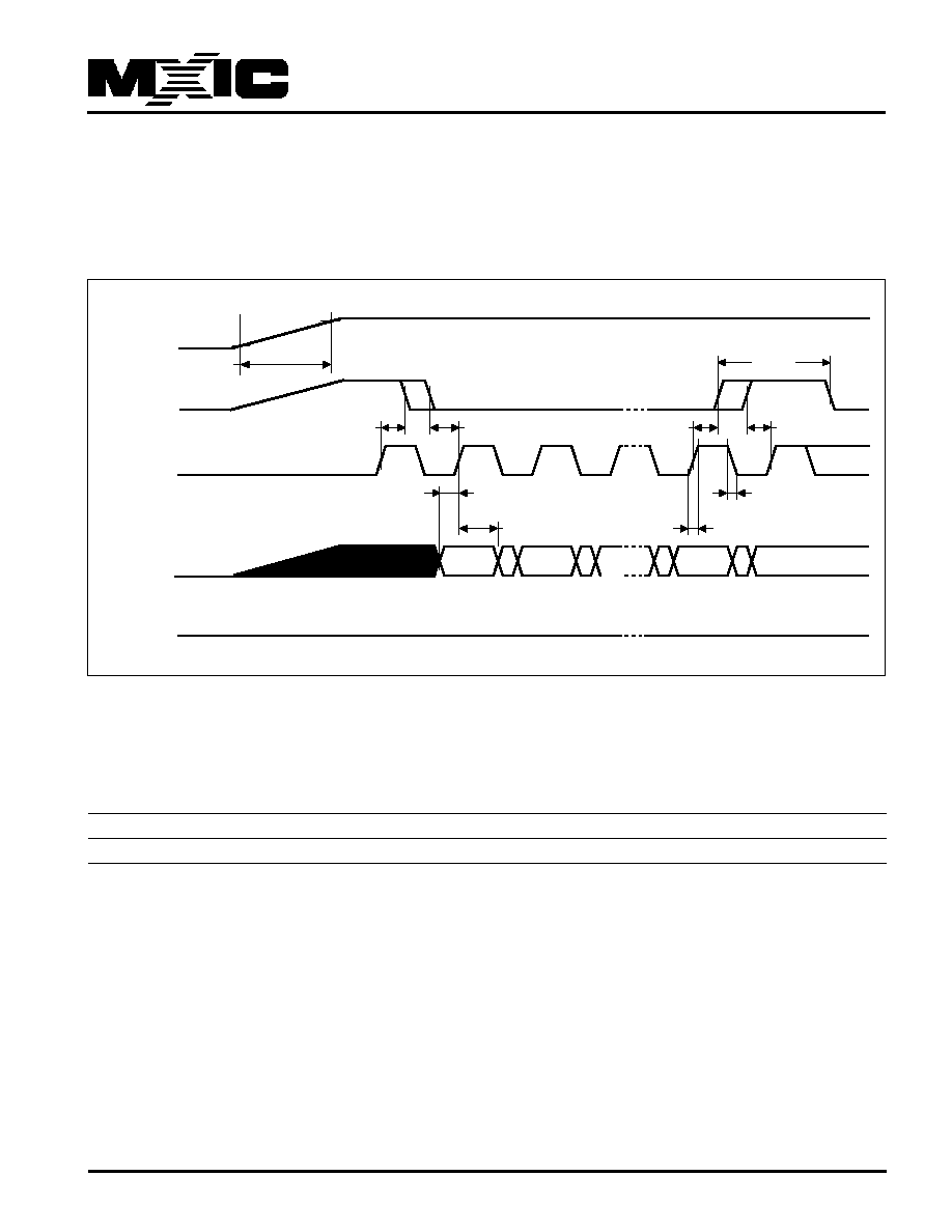
Figure 7. Serial Input Timing
Figure 8. Write Protect Setup and Hold Timing during WRSR when SRWD=1
SCLK
SI
CS#
MSB IN
SO
tDVCH
High Impedance
LSB IN
tSLCH
tCHDX
tCHCL
tCLCH
tSHCH
tSHSL
tCHSH
tCHSL
High Impedance
tWHSL
tSHWL
SCLK
SI
CS#
WP#
SO

24
P/N: PM1236
REV. 1.1, SEP. 30, 2005
MX25L4005
Figure 9. Hold Timing
Figure 10. Output Timing
tCHHL
tHLCH
tHHCH
tCHHH
tHHQX
tHLQZ
SCLK
SO
CS#
SI
HOLD#
LSB OUT
ADDR.LSB IN
tSHQZ
tCH
tCL
tQLQH
tQHQL
tCLQX
tCLQV
tCLQX
tCLQV
SCLK
SO
CS#
SI

25
P/N: PM1236
REV. 1.1, SEP. 30, 2005
MX25L4005
Figure 11. Write Enable (WREN) Instruction Sequence
2
1
3
4
5
6
7
High Impedance
0
Instruction
SCLK
SI
CS#
SO
Figure 12. Write Disable (WRDI) Instruction Sequence
2
1
3
4
5
6
7
High Impedance
0
Instruction
SCLK
SI
CS#
SO
Figure 13. Read Identification (RDID) Instruction Sequence and Data-Out Sequence
2
1
3
4
5
6
7
8
9 10 11 12 13 14 15
Instruction
0
Manufacturer Identification
High Impedance
MSB
15 14 13
3
2
1
0
Device Identification
MSB
7
6
5
3
2
1
0
16 17 18
28 29 30 31
SCLK
SI
CS#
SO

26
P/N: PM1236
REV. 1.1, SEP. 30, 2005
MX25L4005
Figure 14. Read Status Register (RDSR) Instruction Sequence and Data-Out Sequence
Figure 15. Write Status Register (WRSR) Instruction Sequence
2
1
3
4
5
6
7
8
9 10 11 12 13 14 15
High Impedance
Instruction
Status
Register In
0
7
6
5
4
3
2
0
1
MSB
SCLK
SI
CS#
SO
Figure 16. Read Data Bytes (READ) Instruction Sequence and Data-Out Sequence
SCLK
SI
CS#
SO
23
2
1
3
4
5
6
7
8
9 10
28 29 30 31 32 33 34 35
22 21
3
2
1
0
36 37 38
7
6
5
4
3
1
7
0
High Impedance
Data Out 1
Instruction
24-Bit Address
0
MSB
MSB
2
39
Data Out 2
2
1
3
4
5
6
7
8
9 10 11 12 13 14 15
Instruction
0
7
6
5
4
3
2
1
0
Status Register Out
High Impedance
MSB
7
6
5
4
3
2
1
0
Status Register Out
MSB
7
SCLK
SI
CS#
SO

27
P/N: PM1236
REV. 1.1, SEP. 30, 2005
MX25L4005
Figure 17. Read Data Bytes at Higher Speed (FAST_READ) Instruction Sequence and Data-Out
Sequence
23
2
1
3
4
5
6
7
8
9 10
28 29 30 31
22 21
3
2
1
0
High Impedance
Instruction
24 BIT ADDRESS
0
32 33 34
36 37 38 39 40 41 42 43 44 45 46
7
6
5
4
3
2
0
1
DATA OUT 1
Dummy Byte
MSB
7
6
5
4
3
2
1
0
DATA OUT 2
MSB
MSB
7
47
7
6
5
4
3
2
0
1
35
SCLK
SI
CS#
SO
SCLK
SI
CS#
SO
28
P/N: PM1236
REV. 1.1, SEP. 30, 2005
MX25L4005
42
41
43 44 45 46 47 48 49 50
52 53 54 55
40
23
2
1
3
4
5
6
7
8
9 10
28 29 30 31 32 33 34 35
22 21
3
2
1
0
36 37 38
Instruction
24-Bit Address
0
7
6
5
4
3
2
0
1
Data Byte 1
39
51
7
6
5
4
3
2
0
1
Data Byte 2
7
6
5
4
3
2
0
1
Data Byte 3
Data Byte 256
2079
2078
2077
2076
2075
2074
2073
7
6
5
4
3
2
0
1
2072
MSB
MSB
MSB
MSB
MSB
SCLK
CS#
SI
SCLK
CS#
SI
Figure 18. Page Program (PP) Instruction Sequence

29
P/N: PM1236
REV. 1.1, SEP. 30, 2005
MX25L4005
Figure 19. Sector Erase (SE) Instruction Sequence
Note: SE instruction is 20(hex).
Figure 20. Block Erase (BE) Instruction Sequence
24 Bit Address
2
1
3
4
5
6
7
8
9
29 30 31
Instruction
0
23 22
2
0
1
MSB
SCLK
CS#
SI
Note: BE instruction is 52 or D8(hex).
24 Bit Address
2
1
3
4
5
6
7
8
9
29 30 31
Instruction
0
7
6
2
1
0
MSB
7
6
2
1
0
SCLK
CS#
SI

30
P/N: PM1236
REV. 1.1, SEP. 30, 2005
MX25L4005
Figure 21. Chip Erase (CE) Instruction Sequence
2
1
3
4
5
6
7
0
Instruction
SCLK
CS#
SI
Figure 22. Deep Power-down (DP) Instruction Sequence
2
1
3
4
5
6
7
0
t
DP
Deep Power-down Mode
Stand-by Mode
Instruction
SCLK
CS#
SI
Figure 23. Release from Deep Power-down and Read Electronic Signature (RES) Instruction
Sequence and Data-Out Sequence
Note: CE instruction is 60(hex) or C7(hex).
23
2
1
3
4
5
6
7
8
9 10
28 29 30 31 32 33 34 35
22 21
3
2
1
0
36 37 38
7
6
5
4
3
2
0
1
High Impedance
Electronic Signature Out
Instruction
3 Dummy Bytes
0
MSB
Stand-by Mode
Deep Power-down Mode
MSB
t
RES2
SCLK
CS#
SI
SO

31
P/N: PM1236
REV. 1.1, SEP. 30, 2005
MX25L4005
Figure 24. Release from Deep Power-down (RDP) Instruction Sequence
2
1
3
4
5
6
7
0
t
RES1
Stand-by Mode
Deep Power-down Mode
High Impedance
Instruction
SCLK
CS#
SI
SO
Figure 25. Read Electronic Manufacturer & Device ID (REMS) Instruction Sequence and Data-Out
Sequence
15 14 13
3
2
1
0
2
1
3
4
5
6
7
8
9 10
High Impedance
Instruction
2 Dummy Bytes
0
32 33 34
36 37 38 39 40 41 42 43 44 45 46
7
6
5
4
3
2
0
1
Manufacturer ID
ADD (1)
MSB
7
6
5
4
3
2
1
0
Device ID
MSB
MSB
7
47
7
6
5
4
3
2
0
1
35
31
30
29
28
SCLK
SI
CS#
SO
SCLK
SI
CS#
SO
X
Notes:
(1) ADD=00H will output the manufacturer's ID first and ADD=01H will output device ID first
32
P/N: PM1236
REV. 1.1, SEP. 30, 2005
MX25L4005
Figure 26. Power-up Timing
VCC
VCC(min)
VWI
Reset State
of the
Device
Chip Selection Not Allowed
Program, Erase and Write Commands are Rejected by the Device
tVSL
tPUW
time
Read Access allowed
Device fully
accessible
VCC(max)
33
P/N: PM1236
REV. 1.1, SEP. 30, 2005
MX25L4005
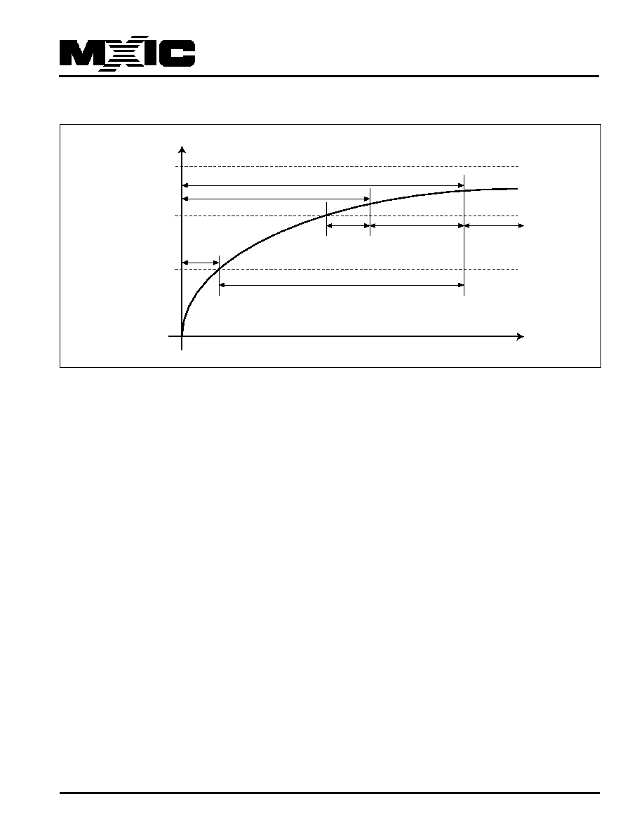
RECOMMENDED OPERATING CONDITIONS
At Device Power-Up
AC timing illustrated in Figure A is recommended for the supply voltages and the control signals at device power-up. If
the timing in the figure is ignored, the device may not operate correctly.
Figure A. AC Timing at Device Power-Up
Notes :
1. Sampled, not 100% tested.
2. For AC spec tCHSL, tSLCH, tDVCH, tCHDX, tSHSL, tCHSH, tSHCH, tCHCL, tCLCH in the figure, please refer to "AC
CHARACTERISTICS" table.
Symbol
Parameter
Notes
Min.
Max.
Unit
tVR
VCC Rise Time
1
0.5
500000
us/V
SCLK
SI
CS#
VCC
MSB IN
SO
tDVCH
High Impedance
LSB IN
tSLCH
tCHDX
tCHCL
tCLCH
tSHCH
tSHSL
tCHSH
tCHSL
tVR
VCC(min)
GND

34
P/N: PM1236
REV. 1.1, SEP. 30, 2005
MX25L4005
ERASE AND PROGRAMMING PERFORMANCE
PARAMETER
Min.
TYP. (1)
Max. (2)
UNIT
Write Status Register Cycle Time
5
15
ms
Sector erase Time
60
120
ms
Block erase Time
1
2
s
Chip Erase Time
3.5
7.5
s
Page Program Time
1.4
5
ms
Erase/Program Cycle
100,000
cycles
Note:
1. Typical program and erase time assumes the following conditions: 25
∞
C, 3.3V, and checker board pattern.
2. Under worst conditions of 70
∞
C and 3.0V.
3. System-level overhead is the time required to execute the first-bus-cycle sequence for the programming command.
4. The maximum chip programming time is evaluated under the worst conditions of 0C, VCC=3.0V, and 100K cycle with
90% confidence level.
MIN.
MAX.
Input Voltage with respect to GND on ACC
-1.0V
12.5V
Input Voltage with respect to GND on all power pins, SI, CS#
-1.0V
2 VCCmax
Input Voltage with respect to GND on SO
-1.0V
VCC + 1.0V
Current
-100mA
+100mA
Includes all pins except VCC. Test conditions: VCC = 3.0V, one pin at a time.
LATCH-UP CHARACTERISTICS

35
P/N: PM1236
REV. 1.1, SEP. 30, 2005
MX25L4005
ORDERING INFORMATION
PART NO.
CLOCK
OPERATING
STANDBY
Temperature PACKAGE
Remark
(MHz)
CURRENT(mA)
CURRENT(uA)
MX25L4005MC-15
70
12
10
0~70
∞
C
8-SOP
(150mil)
MX25L4005MC-15G
70
12
10
0~70
∞
C
8-SOP
Pb-free
(150mil)
MX25L4005M2C-15
70
12
10
0~70
∞
C
8-SOP
(200mil)
MX25L4005M2C-15G
70
12
10
0~70
∞
C
8-SOP
Pb-free
(200mil)
MX25L4005ZMC-15G
70
12
10
0~70
∞
C
8-land SON
Pb-free
(6x5mm)
MX25L4005MI-15
70
12
10
-40~85
∞
C
8-SOP
(150mil)
MX25L4005MI-15G
70
12
10
-40~85
∞
C
8-SOP
Pb-free
(150mil)
MX25L4005M2I-15
70
12
10
-40~85
∞
C
8-SOP
(200mil)
MX25L4005M2I-15G
70
12
10
-40~85
∞
C
8-SOP
Pb-free
(200mil)
MX25L4005ZMI-15G
70
12
10
-40~85
∞
C
8-land SON
Pb-free
(6x5mm)

36
P/N: PM1236
REV. 1.1, SEP. 30, 2005
MX25L4005
PART NAME DESCRIPTION
MX
25
L
15
ZM
C
G
OPTION:
G: Pb-free
blank: normal
SPEED:
15: 70MHz, for SPI
TEMPERATURE RANGE:
C: Commercial (0∞C to 70∞C)
I: Industrial (-40∞C to 85∞C)
PACKAGE:
ZM: SON
M: 150mil 8-SOP
M2: 200mil 8-SOP
DENSITY & MODE:
4005: 4Mb
TYPE:
L: 3V
DEVICE:
25: Serial Flash
4005
37
P/N: PM1236
REV. 1.1, SEP. 30, 2005
MX25L4005
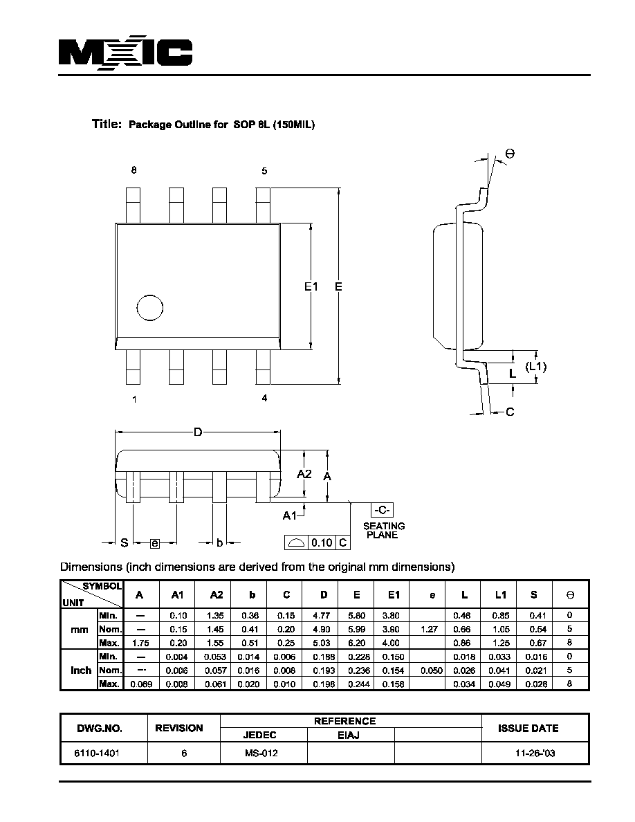
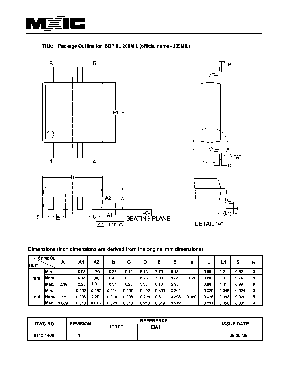
PACKAGE INFORMATION
38
P/N: PM1236
REV. 1.1, SEP. 30, 2005
MX25L4005
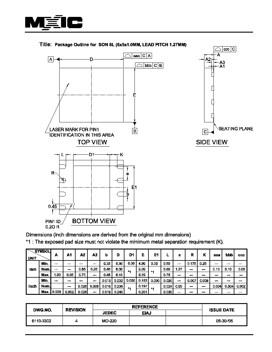
39
P/N: PM1236
REV. 1.1, SEP. 30, 2005
MX25L4005

40
P/N: PM1236
REV. 1.1, SEP. 30, 2005
MX25L4005
REVISION HISTORY
Revision No. Description
Page
Date
1.0
1. Removed "Preliminary"
P1
JUL/14/2005
2. Improved tVSL spec from 30us to 10us
P22
3. To be separated from MX25L4005, MX25L8005 to MX25L4005
All
1.1
1. Standby current is reduced from 50uA(max.) to 10uA(max.)
P1,2,20,35
SEP/30/2005
2. Added description about Pb-free device is RoHS compliant
P1
3. Improved erase speed:
P1,21,34
4KB sector: 90ms(typ.)/270ms(max.)-->60ms(typ.)/120ms(max.)
64KB sector:1s(typ.)/3s(max.)-->1s(typ.)/2s(max.)
chip sector:4.5s(typ.)/10s(max.)-->3.5s(typ.)/7.5s(max.)

MX25L4005
M
ACRONIX
I
NTERNATIONAL
C
O.,
L
TD.
Headquarters:
TEL:+886-3-578-6688
FAX:+886-3-563-2888
Europe Office :
TEL:+32-2-456-8020
FAX:+32-2-456-8021
Hong Kong Office :
TEL:+86-755-834-335-79
FAX:+86-755-834-380-78
Japan Office :
Kawasaki Office :
TEL:+81-44-246-9100
FAX:+81-44-246-9105
Osaka Office :
TEL:+81-6-4807-5460
FAX:+81-6-4807-5461
Singapore Office :
TEL:+65-6346-5505
FAX:+65-6348-8096
Taipei Office :
TEL:+886-2-2509-3300
FAX:+886-2-2509-2200
M
ACRONIX
A
MERICA,
I
NC.
TEL:+1-408-262-8887
FAX:+1-408-262-8810
http : //www.macronix.com
MACRONIX INTERNATIONAL CO., LTD. reserves the right to change product and specifications without notice.