
1
PIN DESCRIPTION
REV. 0.6, JAN. 14, 2002
P/N: PM0768
FEATURES
∑
512Kx 8 organization
∑
Single +5V power supply
∑
+12V programming voltage
∑
Fast access time:70/90/100/120/150 ns
∑
Totally static operation
∑
Completely TTL compatible
∑
Operating current:30mA
∑
Standby current: 100uA
∑
Chip erase time: 2s (typ.)
∑
Chip program time: 25s (typ.)
∑
100 minimum erase/program cycles
∑
Typical fast programming cycle duration 100us/byte
∑
Package type:
- 32 pin plastic DIP
- 32 pin PLCC
- 32 pin TSOP
- 32 pin SOP
PIN CONFIGURATIONS
32 PDIP/SOP
32 PLCC
SYMBOL
PIN NAME
A0~A18
Address Input
Q0~Q7
Data Input/Output
CE
Chip Enable Input
OE
Output Enable Input
VPP
Program Supply Voltage
NC
No Internal Connection
VCC
Power Supply Pin (+5V)
GND
Ground Pin
MX26C4000B
4M-BIT [512K x 8] CMOS
MULTIPLE-TIME-PROGRAMMABLE-EPROM
ADVANCE INFORMATION
MX26C4000B
1
2
3
4
5
6
7
8
9
10
11
12
13
14
15
16
VPP
A16
A15
A12
A7
A6
A5
A4
A3
A2
A1
A0
Q0
Q1
Q2
GND
32
31
30
29
28
27
26
25
24
23
22
21
20
19
18
17
VCC
A18
A17
A14
A13
A8
A9
A11
OE
A10
CE
Q7
Q6
Q5
Q4
Q3
1
4
5
9
13
14
17
20
21
25
29
32
30
A14
A13
A8
A9
A11
OE
A10
CE
Q7
A7
A6
A5
A4
A3
A2
A1
A0
Q0
Q1
Q2
GND
Q3
Q4
Q5
Q6
A12
A15
A16
VPP
VCC
A18
A17
MX26C4000B
32 TSOP
A11
A9
A8
A13
A14
A17
A18
VCC
VPP
A16
A15
A12
A7
A6
A5
A4
1
2
3
4
5
6
7
8
9
10
11
12
13
14
15
16
OE
A10
CE
Q7
Q6
Q5
Q4
Q3
GND
Q2
Q1
Q0
A0
A1
A2
A3
32
31
30
29
28
27
26
25
24
23
22
21
20
19
18
17
MX26C4000B
GENERAL DESCRIPTION
The MX26C4000B is a 5V only, 4M-bit, MTP EPROM
TM
(Multiple Time Programmable Read Only Memory). It is
organized as 512K words by 8 bits per word, operates
from a single + 5 volt supply, has a static standby mode,
and features fast single address location programming.
All programming signals are TTL levels, requiring a
single pulse. It is design to be programmed and erased
by an EPROM programmer or on-board. The
MX26C4000B supports a intelligent fast programming
algorithm which can result in programming time of less
than one minute.
This MTP EPROM
TM
is packaged in industry standard 32
pin dual-in-line packages, 32 lead PLCC, 32 lead SOP
and 32 lead TSOP packages.
2
REV. 0.6, JAN. 14, 2002
P/N: PM0768
MX26C4000B
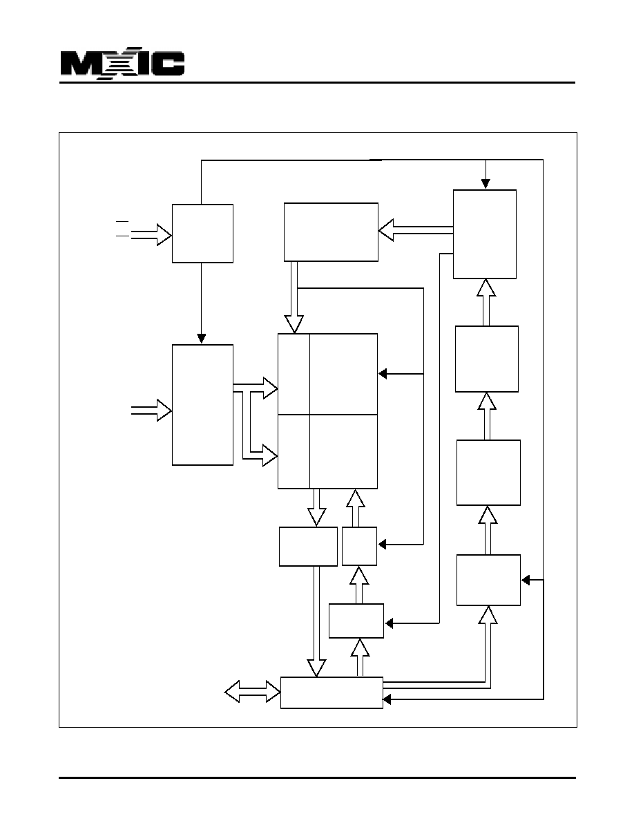
BLOCK DIAGRAM
CONTROL
INPUT
LOGIC
PROGRAM/ERASE
HIGH VOLTAGE
WRITE
STATE
MACHINE
(WSM)
STATE
REGISTER
MX26C4000B
FLASH
ARRAY
X-DECODER
ADDRESS
LATCH
AND
BUFFER
Y-PASS GATE
Y
-DECODER
ARRAY
SOURCE
HV
COMMAND
DATA
DECODER
COMMAND
DATA LATCH
I/O BUFFER
PGM
DATA
HV
PROGRAM
DATA LATCH
SENSE
AMPLIFIER
Q0-Q7
A0-A18
CE
OE

3
REV. 0.6, JAN. 14, 2002
P/N: PM0768
MX26C4000B
FUNCTIONAL DESCRIPTION
When the MX26C4000B is delivered, or it is erased, the
chip has all 4M bits in the "ONE", or HIGH state.
"ZEROs" are loaded into the MX26C4000B through the
procedure of programming.
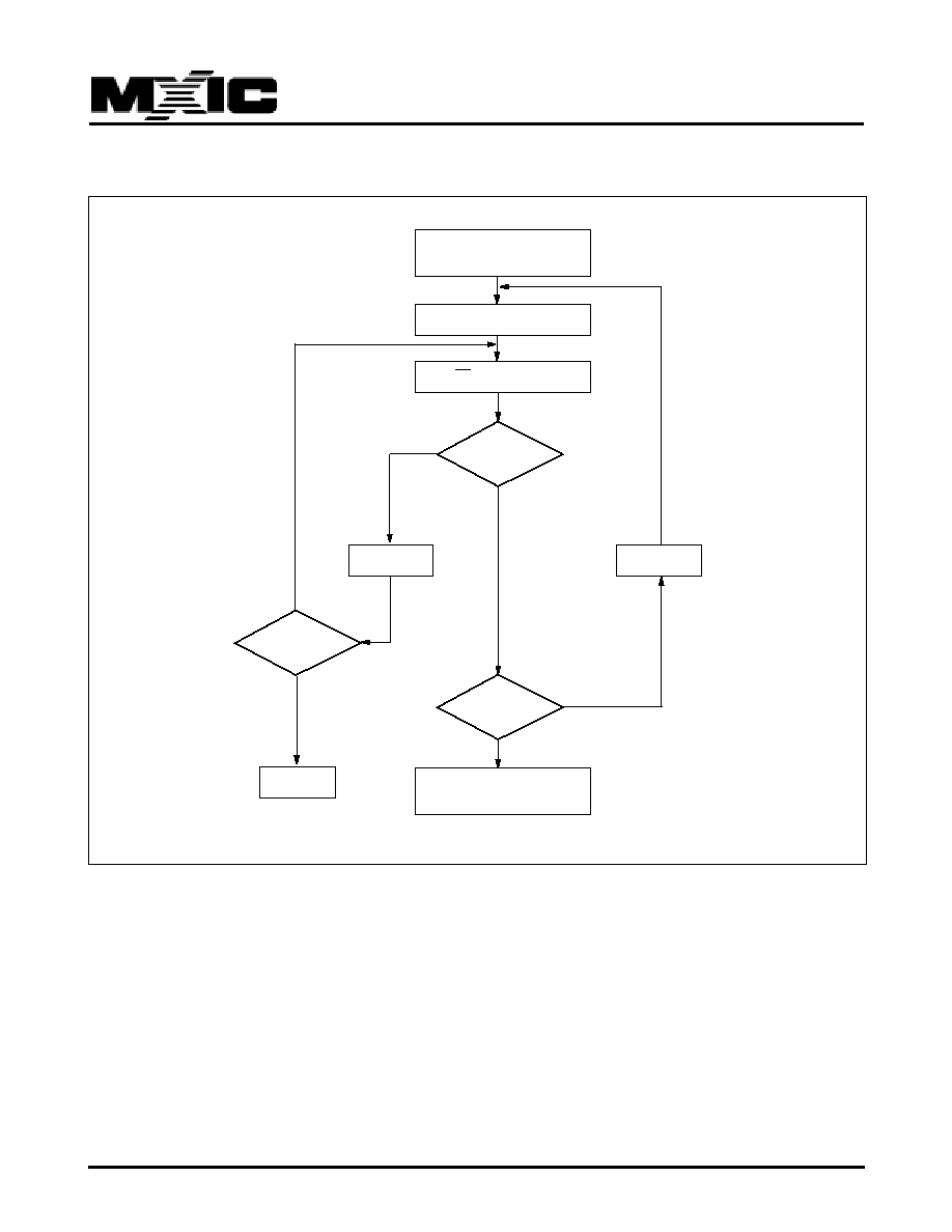
ERASE ALGORITHM
The MX26C4000B do not required preprogramming
before an erase operation. The erase algorithm is a close
loop flow to simultaneously erase all bits in the entire
array. Erase operation starts with the initial erase
operation. Erase verification begins at address 0000H
by reading data FFH from each byte. If any byte fails
to erase. the entire chip is reerased. to a maximum for
10 pulse counts of 500ms duration for each pulse. The
maximum cumulative erase time is 3s. However. the
device is usually erased in no more than 3 pulses. Erase
verification time can be reduced by storing the address
of the last byte that failed. Following the next erase
operation verification may start at the stored address
location. JEDEC standard erase algorithm can also be
used. But erase time will increase by performing the
unnecessary preprogramming.
PROGRAM ALGORITHM
The device is programmed byte by byte. A maximum
of 25 pulses. each of 100us duration is allowed for each
byte being programmed. The byte may be programmed
sequentially or by random. After each program pulse,
a program verify is done to determine if the byte has
been successfully programmed.
Programming then proceeds to the next desired byte
location. JEDEC standard program algorithms can be
used.
DATA WRITE PROTECTION
The design of the device protects against accidental
erasure or programming. The internal state machine is
automatically reset to the read mode on power-up. Using
control register architecture, alteration of memory can
only occur after completion of proper command
sequences. The command register is only active when V
PP
is at high voltage. when V
PP
= V
PPL
, the device defaults
to the Read Mode. Robust design features prevent
inadvertent write cycles resulting from V
CC
power-up and
power-down transitions or system noise. To avoid initiation
of write cycle during V
CC
power-up, a write cycle is locked
out for V
CC
less than 4V. The two- command program and
erase write sequence to the command register provide
additional software protection against spurious data
changes.
PROGRAM VERIFY MODE
Verification should be performed on the programmed bits
to determine that they were correctly programmed.
Verification should be performed with OE and CE, at
VIL, and VPP at its programming voltage.
ERASE VERIFY MODE
Verification should be performed on the erased chip to
determine that the whole chip(all bits) was correctly
erased. Verification should be performed with OE and
CE at VIL, and VCC = 5V, VPP = 12.5V
AUTO IDENTIFY MODE
The auto identify mode allows the reading out of a binary
code from MTP EPROM that will identify its
manufacturer and device type. This mode is intended
for use by programming equipment for the purpose of
automatically matching the device to be programmed
with its corresponding programming algorithm. This
mode is functional in the 25
∞
C
±
5
∞
C ambient temperature
range that is required when programming the
MX26C4000B.
To activate this mode, the programming equipment must
force 12.0
±
0.5 V on address line A9 of the device.
Two identifier bytes may then be sequenced from the
device outputs by toggling address line A0 from VIL
to VIH. All other address lines must be held at VIL
during auto identify mode.
Byte 0 ( A0 = VIL) represents the manufacturer code,
and byte 1 (A0 = VIH), the device identifier code. For
the MX26C4000B, these two identifier bytes are given
in the Mode Select Table. All identifiers for manufacturer
and device codes will possess odd parity, with the MSB
(DQ7) defined as the parity bit.

4
REV. 0.6, JAN. 14, 2002
P/N: PM0768
MX26C4000B
READ MODE
The MX26C4000B has two control functions, both of
which must be logically satisfied in order to obtain data
at the outputs. Chip Enable (CE) is the power control
and should be used for device selection. Output Enable
(OE) is the output control and should be used to gate
data to the output pins, independent of device selection.
Assuming that addresses are stable, address access
time (tACC) is equal to the delay from CE to output (tCE).
Data is available at the outputs tOE after the falling edge
of OE, assuming that CE has been LOW and addresses
have been stable for at least tACC - tOE.
STANDBY MODE
The MX26C4000B has a CMOS standby mode which
reduces the maximum VCC current to 100 uA. It is
placed in CMOS standby when CE is at VCC
±
0.3 V.
The MX26C4000B also has a TTL-standby mode which
reduces the maximum VCC current to 1.5 mA. It is
placed in TTL-standby when CE is at VIH. When in
standby mode, the outputs are in a high-impedance
state, independent of the OE input.
SYSTEM CONSIDERATIONS
During the switch between active and standby
conditions, transient current peaks are produced on the
rising and falling edges of Chip Enable. The magnitude
of these transient current peaks is dependent on the
output capacitance loading of the device. At a minimum,
a 0.1 uF ceramic capacitor (high frequency, low inherent
inductance) should be used on each device between
VCC and GND to minimize transient effects. In addition,
to overcome the voltage drop caused by the inductive
effects of the printed circuit board traces on EPROM
arrays, a 4.7 uF bulk electrolytic capacitor should be
used between VCC and GND for each of the eight
devices. The location of the capacitor should be close
to where the power supply is connected to the array.
OUTPUT DISABLE
Output is disabled when OE is at logre high. When in
output disabled all circuitry is enabled. Except the output
pins are in a high impedance state(Hi-Z).
5
REV. 0.6, JAN. 14, 2002
P/N: PM0768
MX26C4000B
Table 1: BUS OPERATIONS
Mode
VPP(1)
A0
A9
CE
OE
Q0~Q7
Read
VPPL
A0
A9
VIL
VIL
Data Out
Output Disable
VPPL
X
X
VIL
VIH
Hi-Z
Standby
VPPL
X
X
VIH
X
Hi-Z
Manufacturer Identification
VPPL
VIL
VID(2)
VIL
VIL
Data=C2H
Device Identification
VPPL
VIH
VID(2)
VIL
VIL
Data=C0H
Program
VPPH
A0
X
VIL
VIH
Data In
Verify
VPPH
A0
X
VIH
VIL
Data Out
Program Inhibit
VPPH
X
X
VIH
VIH
Hi-Z
Note:
1. Refer to DC Characteristics. When VPP=VPPL memory contents can be read but not written or erased.
2. VID is the intelligent identifier high voltage. Refer to DC Characteristics.
3. Read operations with VPP=VPPH may access array data or the intelligent identifier codes.
4. With VPP at high voltage the standby current equals ICC+IPP(standby).
5. Refer to Table 2 for vaild data-in during a write operation.
6. X can be VIL or VIH.
6
REV. 0.6, JAN. 14, 2002
P/N: PM0768
MX26C4000B
PROGRAMMING ALGORITHM FLOW CHART
VCC=6.25V
VPP=12.75V
Check All Bytes
1st:VCC=6V
2nd:VCC=4.2V
n=0
CE=100us Pulse
N=N+1
next
Address
Failed
YES
YES
YES
NO
NO
NO
Verify
Last
Address
n=25

7
REV. 0.6, JAN. 14, 2002
P/N: PM0768
MX26C4000B
ERASE ALGORITHM FLOW CHART
START
n=0
Chip Erase pulse
A9=12.5V
VCC=5V
VPP=12.5V
Erase:
A9=VIL or VIH
VCC=5V
VPP=12.5V
Verify:
N=N+1
Faild
Passed
Yes
No
No
Yes
Erase Verify
n=10
8
REV. 0.6, JAN. 14, 2002
P/N: PM0768
MX26C4000B
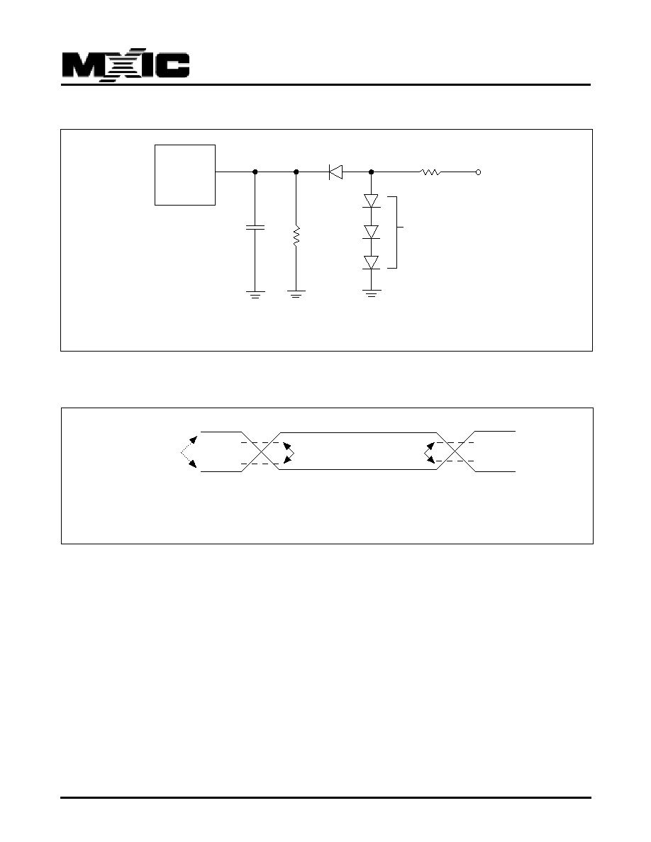
SWITCHING TEST CIRCUITS
SWITCHING TEST WAVEFORMS
DEVICE
UNDER
TEST
DIODES = IN3064
OR EQUIVALENT
CL = 100 pF including jig capacitance
6.2K ohm
1.8K ohm
+5V
CL
2.0V
0.8V
TEST POINTS
INPUT
2.0V
0.8V
OUTPUT
AC TESTING: AC driving levels are 2.4V/0.4V for commercial grade.
Input pulse rise and fall times are equal to or less than 10ns.
AC driving levels

9
REV. 0.6, JAN. 14, 2002
P/N: PM0768
MX26C4000B
NOTICE:
Stresses greater than those listed under ABSOLUTE
MAXIMUM RATINGS may cause permanent damage to
the device. This is a stress rating only and functional
operation of the device at these or any other conditions
above those indicated in the operational sections of this
specification is not implied. Exposure to absolute
maximum rating conditions for extended period may
affect reliability.
NOTICE:
Specifications contained within the following tables are
subject to change.
ABSOLUTE MAXIMUM RATINGS
RATING
VALUE
Ambient Operating Temperature -40
o
C to 85
o
C
Storage Temperature
-65
o
C to 125
o
C
Applied Input Voltage
-0.5V to 7.0V
Applied Output Voltage
-0.5V to VCC + 0.5V
VCC to Ground Potential
-0.5V to 7.0V
A9 & VPP
-0.5V to 13.5V
CAPACITANCE
TA = 25
o
C, f = 1.0 MHz (Sampled only)
SYMBOL
PARAMETER
TYP.
MAX.
UNIT
CONDITIONS
CIN
Input Capacitance
6
pF
VIN = 0V
COUT
Output Capacitance
12
pF
VOUT = 0V
CVPP
VPP Capacitance
18
25
pF
VPP = 0V
DC CHARACTERISTICS
TA = -45
∞
C ~ 85
∞
C, VCC=5V
±
10%
SYMBOL
PARAMETER
MIN.
MAX.
UNIT CONDITIONS
VIL
Input Low Voltage
-0.3
0.8
V
VIH
Input High Voltage
2.0
VCC + 1
V
VOL
Output Low Voltage
0.4
V
IOL = 2.1mA, VCC=VCC MIN
VOH
Output High Voltage (TTL)
2.4
V
IOH = -0.4mA
VOH
Output High Voltage (CMOS)
VCC-0.7V
V
IOH = -0.1mA
ICC1
VCC Active Current
30
mA
CE = VIL, OE=VIH, f=5MHz
ISB
VCC Standby Current (CMOS)
100
uA
CE=VCC+0.2V, VCC=VCC MAX
ISB
VCC Standby Current (TTL)
1
mA
CE=VIH, VCC=VCC MAX
IPP
VPP Supply Current (Program)
10
uA
CE=WE=VIL, OE=VIH
ILI
Input Leakage Current
-10
10
uA
VIN = 0 to 5.5V
ILO
Output Leakage Current
-10
10
uA
VOUT = 0 to 5.5V
VCC1
Fast Programming Supply Voltage
6.0
6.5
V
VPP1
Fast Programming Voltage
12.5
13.0
V
MX26C4000B
-90
-100
-120
-150
Operating Temperature Industrial
-40
∞
C to 85
∞
C
-40
∞
C to 85
∞
C
-40
∞
C to 85
∞
C
-40
∞
C to 85
∞
C
Vcc Power Supply
5V
±
10%
5V
±
10%
5V
±
10%
5V
±
10%
DC/AC OPERATING CONDITION FOR READ OPERATION
10
REV. 0.6, JAN. 14, 2002
P/N: PM0768
MX26C4000B
AC RAED CHARACTERISTICS OVER OPERATING RANGE WITH VPP=VCC
Symbol
Parameter
70
90
100
120
150
Unit
Jeded STD
MIN MAX MIN MAX MIN MAX MIN MAX MIN MAX
tAVAV TRC
Read Cycle Time
70
90
100
120
150
ns
tELQV TCE
CE Access Time
0
70
0
90
0
100
0
120
0
150
ns
tAVQV TACC Address Access Time
0
70
0
90
0
100
0
120
0
150
ns
tGLQV TOE
OE Access Time
0
35
0
40
0
45
0
50
0
65
ns
tELQX TLZ
CE to Output in Low Z(Note 1)
0
0
0
0
0
ns
tEHQZ TDF
Chip Disable to Output in
0
30
0
30
0
35
0
35
0
50
ns
High Z (Note 2)
tGLQX TOLZ OE to Output in Low Z (Note 1)
0
0
0
0
0
ns
tGHQZ TDF
Output Disable to Output in
0
30
0
30
0
35
0
35
0
50
ns
High Z (Note 1)
tAXQX TOH
Output Hold from Address,
0
0
0
0
0
ns
CE or OE, change
tVCS
TVCS VCC Setup Time to Valid Read
50
50
50
50
50
us
(Note 2)
Note:
1. Sampled: not 100% tested.
2. Guaranteed by design. not tested.

11
REV. 0.6, JAN. 14, 2002
P/N: PM0768
MX26C4000B
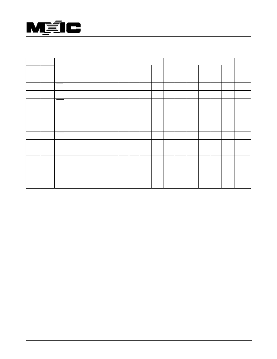
AC WAVEFORMS FOR READ OPERATIONS
Address
CE
OE
Data
VCC
tAXQX(tOH)
tGHQZ(tDF)
tEHQZ(tDF)
tAVAV(tRC)
tGLQV(tOE)
tELQX(tLZ)
tGLQX(tOLZ)
tELQV(tCE)
tVCS
tAVQV(tACC)
High Z
5.0V
0V
Power-Up Standby
Device and
Address Selection
Outputs
enabled
Data Valid
Standby Power-Up
High Z
Addresses Stable
Output Valid
12
REV. 0.6, JAN. 14, 2002
P/N: PM0768
MX26C4000B
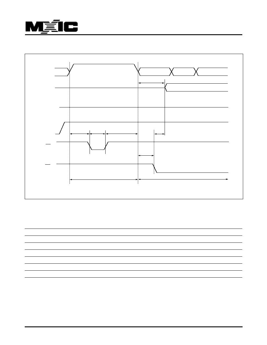
AC WAVEFORMS FOR ERASE OPERATIONS
Table 2. Erasing Mode AC Characteristics
(1)
(TA=25
∞
∞
∞
∞
∞
C; VCC=5V
±
±
±
±
±
0.25V; VPP=12.5V
±
±
±
±
±
0.25V)
Symbol
Parameter
Min
Max
Unit
tA9HEL
A9 High to Chip Enable Low
2
us
tAVGL
Address Valid to Output Enable Low
2
us
tAVQV
Address Valid to Data Valid
100
ns
tEHA9L
Chip Enable High to A9 Low
2
us
tER
First Erase Time
500
ms
tGLQV
Output Enable Low to Data Valid
30
ns
(1)
VCC must be applied simultaneously with or before VPP and removed simultaneously or after VPP.
A9
Q0~Q7
VCC
VPP
CE
OE
tAVQ
tGLQ
tEH
tE
tHE
Chip Erase
5V
12V
All Matrix Verif
tAVG
Valid
13
REV. 0.6, JAN. 14, 2002
P/N: PM0768
MX26C4000B
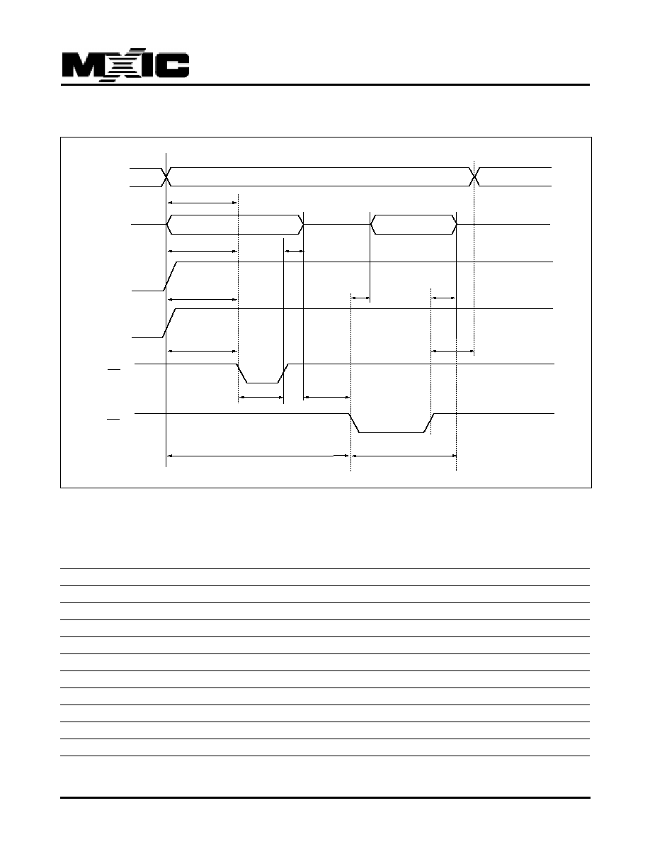
AC WAVEFORMS FOR PROGRAMMING OPERATIONS
Table 3. Programming Mode AC Characteristics
(1)
(TA=25
∞
∞
∞
∞
∞
C; VCC=6.25V
±
±
±
±
±
0.25V; VPP=12.5V
±
±
±
±
±
0.25V)
Symbol
Alt
Parameter
Min
Max
Unit
tAVPL
tAS
Address Valid to Chip Enable Low
2
us
TQVEL
tDS
Input Valid to Chip Enable Low
2
us
TVPHEL
tVPS
VPP High to Chip Enable Low
2
us
TVCHEL
tVCS
VCC High to Chip Enable Low
2
us
TELEH
tPW
Chip Enable Program Pulse Wodth
95
105
us
TEHQX
tDH
Chip Enable High to Input Transition
2
us
TQXGL
tOES
Input Transition to Output Enable Low
2
us
TGLQV
tOE
Output Enable Low to Output Valid
100
ns
TGHQZ
tDFP
Output Enable High to Output Hi-Z
0
130
ns
TGHAX
tAH
Output Enable High to Address Transition
0
ns
(1)
VCC must be applied simultaneously with or before VPP and removed simultaneously or after VPP.
(2)
Sampled only, not 100% tested.
A0-A18
Q0~Q7
VCC
VPP
CE
OE
tAVPL
tQVEL
tEHQX
tGLQV
tGHQZ
tVPHEL
tVCHEL
PROGRAM
VERIFY
tELEH
tQXGL
VALID
DATA OUT
DATA IN
tGHAX
14
REV. 0.6, JAN. 14, 2002
P/N: PM0768
MX26C4000B
ORDERING INFORMATION
PLASTIC PACKAGE
PART NO.
ACCESS TIME(ns)
OPERATING
STANDBY
OPERATING
PACKAGE
Current MAX.(mA)
Current MAX.(uA)
TEMPERATURE
MX26C4000BPC-90
90
30
100
0
∞
C to 70
∞
C
32 Pin DIP
MX26C4000BQC-90
90
30
100
0
∞
C to 70
∞
C
32 Pin PLCC
MX26C4000BMC-90
90
30
100
0
∞
C to 70
∞
C
32 Pin SOP
MX26C4000BTC-90
90
30
100
0
∞
C to 70
∞
C
32 Pin TSOP
MX26C4000BPC-10
100
30
100
0
∞
C to 70
∞
C
32 Pin DIP
MX26C4000BQC-10
100
30
100
0
∞
C to 70
∞
C
32 Pin PLCC
MX26C4000BMC-10
100
30
100
0
∞
C to 70
∞
C
32 Pin SOP
MX26C4000BTC-10
100
30
100
0
∞
C to 70
∞
C
32 Pin TSOP
MX26C4000BPC-12
120
30
100
0
∞
C to 70
∞
C
32 Pin DIP
MX26C4000BQC-12
120
30
100
0
∞
C to 70
∞
C
32 Pin PLCC
MX26C4000BMC-12
120
30
100
0
∞
C to 70
∞
C
32 Pin SOP
MX26C4000BTC-12
120
30
100
0
∞
C to 70
∞
C
32 Pin TSOP
MX26C4000BPC-15
150
30
100
0
∞
C to 70
∞
C
32 Pin DIP
MX26C4000BQC-15
150
30
100
0
∞
C to 70
∞
C
32 Pin PLCC
MX26C4000BMC-15
150
30
100
0
∞
C to 70
∞
C
32 Pin SOP
MX26C4000BTC-15
150
30
100
0
∞
C to 70
∞
C
32 Pin TSOP
MX26C4000BPI-90
90
30
100
-40
∞
C to 85
∞
C
32 Pin DIP
MX26C4000BQI-90
90
30
100
-40
∞
C to 85
∞
C
32 Pin PLCC
MX26C4000BMI-90
90
30
100
-40
∞
C to 85
∞
C
32 Pin SOP
MX26C4000BTI-90
90
30
100
-40
∞
C to 85
∞
C
32 Pin TSOP
MX26C4000BPI-10
100
30
100
-40
∞
C to 85
∞
C
32 Pin DIP
MX26C4000BQI-10
100
30
100
-40
∞
C to 85
∞
C
32 Pin PLCC
MX26C4000BMI-10
100
30
100
-40
∞
C to 85
∞
C
32 Pin SOP
MX26C4000BTI-10
100
30
100
-40
∞
C to 85
∞
C
32 Pin TSOP
MX26C4000BPI-12
120
30
100
-40
∞
C to 85
∞
C
32 Pin DIP
MX26C4000BQI-12
120
30
100
-40
∞
C to 85
∞
C
32 Pin PLCC
MX26C4000BMI-12
120
30
100
-40
∞
C to 85
∞
C
32 Pin SOP
MX26C4000BTI-12
120
30
100
-40
∞
C to 85
∞
C
32 Pin TSOP
MX26C4000BPI-15
150
30
100
-40
∞
C to 85
∞
C
32 Pin DIP
MX26C4000BQI-15
150
30
100
-40
∞
C to 85
∞
C
32 Pin PLCC
MX26C4000BMI-15
150
30
100
-40
∞
C to 85
∞
C
32 Pin SOP
MX26C4000BTI-15
150
30
100
-40
∞
C to 85
∞
C
32 Pin TSOP
15
REV. 0.6, JAN. 14, 2002
P/N: PM0768
MX26C4000B
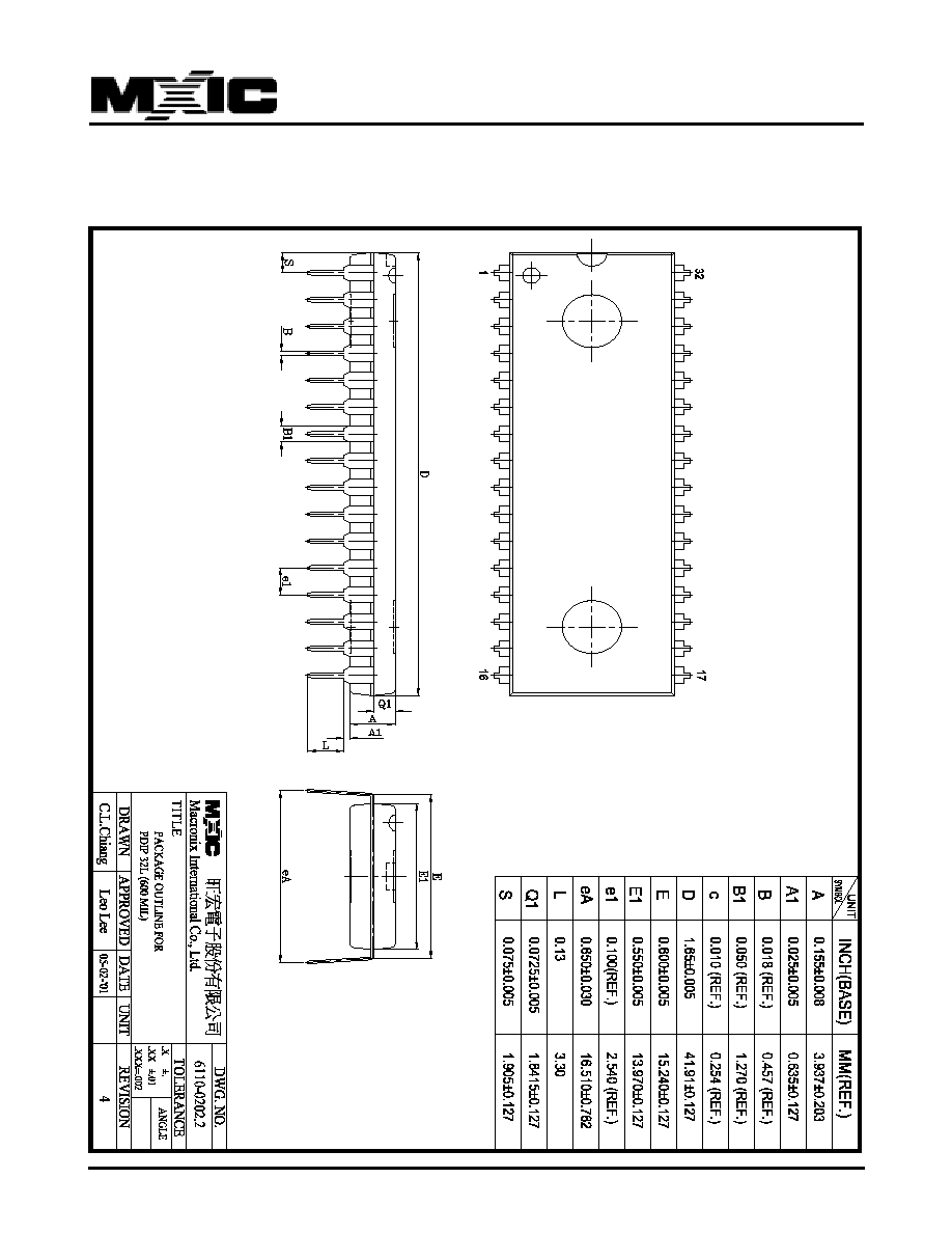
PACKAGE INFORMATION
32-PIN PLASTIC DIP(600 mil)
16
REV. 0.6, JAN. 14, 2002
P/N: PM0768
MX26C4000B
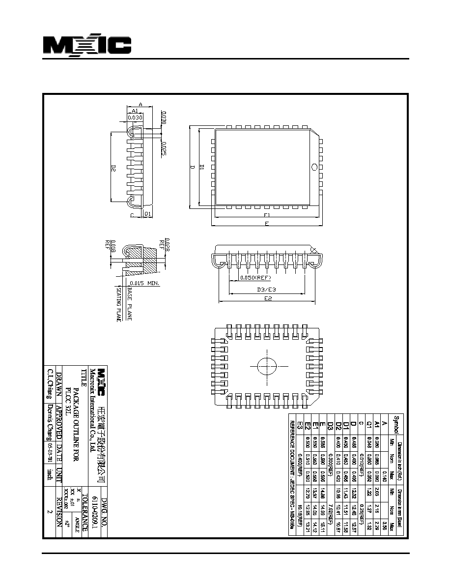
32-PIN PLASTIC LEADED CHIP CARRIER (PLCC)

17
REV. 0.6, JAN. 14, 2002
P/N: PM0768
MX26C4000B
32-PIN PLASTIC TSOP

18
REV. 0.6, JAN. 14, 2002
P/N: PM0768
MX26C4000B
32-PIN PLASTIC SOP (450 mil)

19
REV. 0.6, JAN. 14, 2002
P/N: PM0768
MX26C4000B
REVISION HISTORY
Revision No. Description
Page
Date
0.1
To add erase/program cycle
P1
DEC/18/2000
Change title from MX26C4000A to MX26C4000B
All
0.2
To added 32SOP/TSOP types package and access time 150ns
P1,10,11,16,18 MAR/27/2001
Modify device ID old 32H-->New C0H
P5
Modify read ID method
P4,5,6,12
Modify erase/program cycle from 100 to 50
P1
Modify VCC Standby Current(TTL) from 1mA to 1.5mA
P10
0.3
To added VCC1 & VPP1 to DC Characteristics Table
P10
APR/23/2001
Modify Package Information
P17~20
0.4
To added chip erase time / chip program time
P1
JUL/04/2001
Modify Package Information
P17~20
0.5
Modify the Programming Operations Timing Waveforms
P15
OCT/04/2001
0.6
1.Cancel the command mode
P12
JAN/14/2002
2.Modify the cycle time from 50-->100
P1
3.Modify the erase/program operation timing waveform and
P6,7,12,13
flowchart

MX26C4000B
M
ACRONIX
I
NTERNATIONAL
C
O.,
L
TD.
HEADQUARTERS:
TEL:+886-3-578-6688
FAX:+886-3-563-2888
EUROPE OFFICE:
TEL:+32-2-456-8020
FAX:+32-2-456-8021
JAPAN OFFICE:
TEL:+81-44-246-9100
FAX:+81-44-246-9105
SINGAPORE OFFICE:
TEL:+65-348-8385
FAX:+65-348-8096
TAIPEI OFFICE:
TEL:+886-2-2509-3300
FAX:+886-2-2509-2200
M
ACRONIX
A
MERICA,
I
NC.
TEL:+1-408-453-8088
FAX:+1-408-453-8488
CHICAGO OFFICE:
TEL:+1-847-963-1900
FAX:+1-847-963-1909
http : //www.macronix.com
MACRONIX INTERNATIONAL CO., LTD. reserves the right to change product and specifications without notice.