
1
P/N:PM0914
REV. 0.1, NOV. 20, 2002
MX26L6413
64M-BIT [4M x 16] CMOS
MULTIPLE-TIME-PROGRAMMABLE EPROM
ADVANCED INFORMATION
FEATURES
∑
4,194,304 x 16 byte structure
∑
Single Power Supply Operation
- 2.7 to 3.6 volt for read, erase andprogram
operation
∑
Low Vcc write inhibit is equal to or less than 2.5V
∑
Compatible with JEDEC standard
∑
High Performance
- Fast access time: 90/120ns (typ.)
- Fast program time: 140s/chip (typ.)
- Fast erase time: 150s/chip (typ.)
∑
Low Power Consumption
- Low active read current: 17mA (typ.) at 5MHz
- Low standby current: 30uA (typ.)
∑
Minimum 100 erase/program cycle
∑
Status Reply
- Data polling & Toggle bits provide detection of
program and erase operation completion
∑
12V ACC input pin provides accelerated program
capability
∑
Output voltages and input voltages on the device is
deterined by the voltage on the VI/O pin.
- VI/O voltage range:1.65V~3.6V
∑
10 years data retention
∑
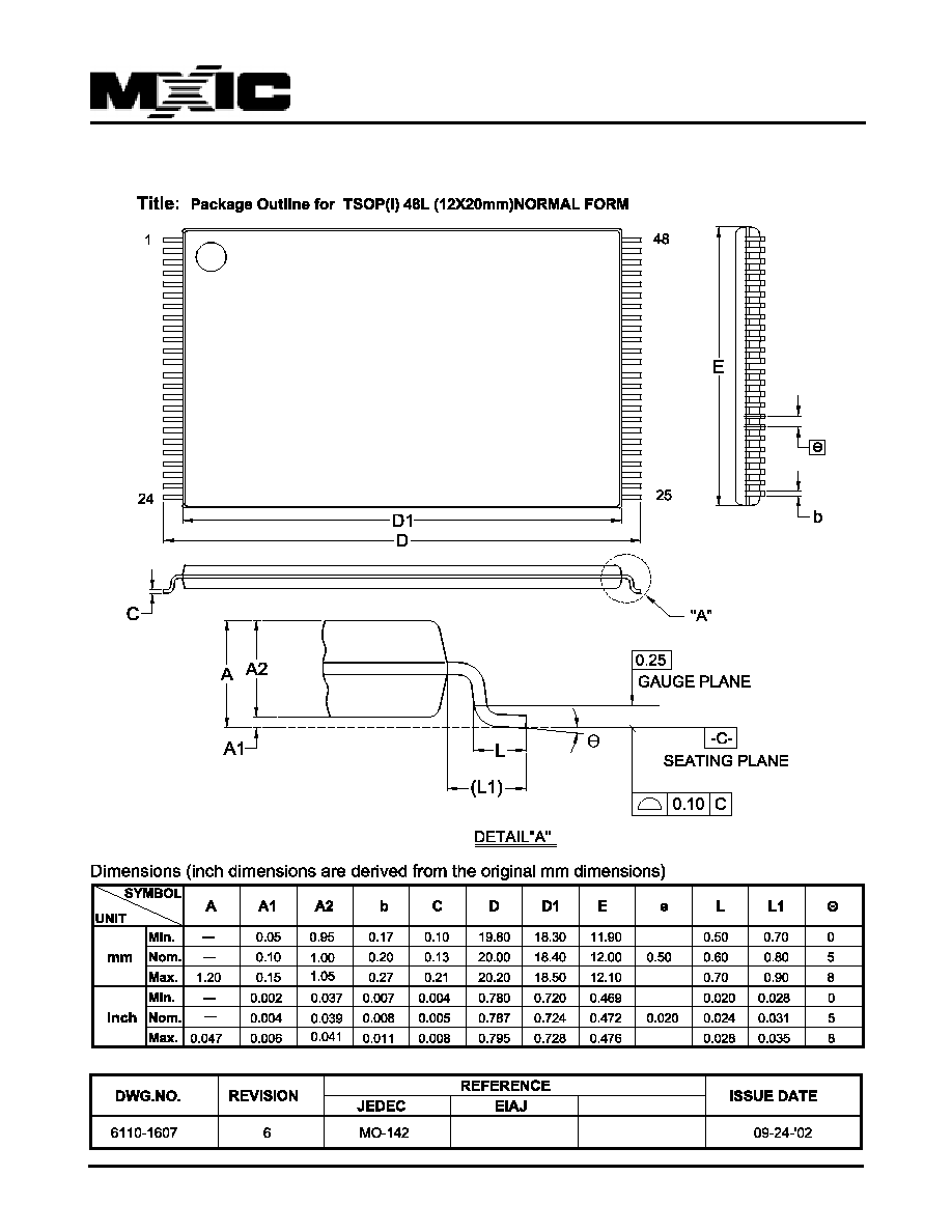
Package
- 48-Pin TSOP
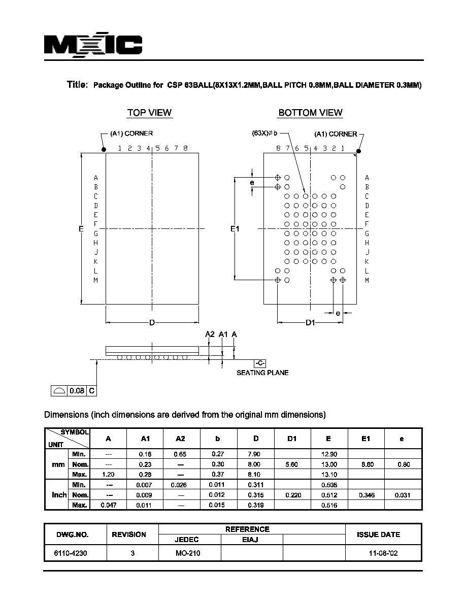
- 63-Ball CSP
GENERAL DESCRIPTION
The MX26L6413 is a 64M bit MTP EPROM
TM
organized
as 4M bytes of 16 bits. MXIC's MTP EPROM
TM
offer the
most cost-effective and reliable read/write non-volatile
random access memory. The MX26L6413 is packaged in
48-pin TSOP, 48-ball CSP amd 63-ball CSP. It is
designed to be reprogrammed and erased in system or in
standard EPROM programmers.
The standard MX26L6413 offers access time as fast as
90ns, allowing operation of high-speed microprocessors
without wait states. To eliminate bus contention, the
MX26L6413 has separate chip enable (CE) and output
enable OE controls. MXIC's MTP EPROM
TM
augment
EPROM functionality with in-circuit electrical erasure and
programming. The MX26L6413 uses a command register
to manage this functionality.
MXIC's MTP EPROM
TM
technology reliably stores
memory contents even after 100 erase and program
cycles. The MXIC cell is designed to optimize the erase
and program mechanisms. In addition, the combination of
advanced tunnel oxide processing and low internal
electric fields for erase and programming operations
produces reliable cycling.
The MX26L6413 uses a 2.7V to 3.6V VCC supply to
perform the High Reliability Erase and auto Program/
Erase algorithms.
The highest degree of latch-up protection is achieved with
MXIC's proprietary non-epiprocess. Latch-up protection
is proved for stresses up to 100 milliamps on address and
data pin from -1V to VCC +1V.

2
P/N:PM0914
REV. 0.1, NOV. 20, 2002
MX26L6413
PIN CONFIGURATION
63 CSP Ball pitch=0.8mm for MX26L6413XB (TOP view, Ball down)
A13
A9
WE
NC
A7
A3
A
* Ball are shorted together via the substrate but not connected to the die.
8
7
6
5
4
3
2
1
B
C
D
E
F
G
H
J
K
L
M
A12
NC
NC
A8
RESET
ACC
A17
A4
A14
A10
A21
A18
A6
A2
A15
A11
A19
A20
A5
A1
A16
Q7
Q5
Q2
Q0
A0
VIO
Q14
Q12
Q10
Q8
CE
Q15
Q13
VCC
Q11
Q9
OE
GND
Q6
Q4
Q3
Q1
GND
NC*
NC*
NC*
NC*
13.0 mm
8.0 mm
NC*
NC*
NC
NC
NC*
NC*
NC*
NC*
NC*
48 TSOP
A15
A14
A13
A12
A11
A10
A9
A8
A21
A20
WE
RESET
ACC
VCC
A19
A18
A17
A7
A6
A5
A4
A3
A2
A1
1
2
3
4
5
6
7
8
9
10
11
12
13
14
15
16
17
18
19
20
21
22
23
24
A16
V
I/O
GND
Q15
Q7
Q14
Q6
Q13
Q5
Q12
Q4
V
CC
Q11
Q3
Q10
Q2
Q9
Q1
Q8
Q0
OE
GND
CE
A0
48
47
46
45
44
43
42
41
40
39
38
37
36
35
34
33
32
31
30
29
28
27
26
25
MX26L6413

3
P/N:PM0914
REV. 0.1, NOV. 20, 2002
MX26L6413
SYMBOL
PIN NAME
A0~A21
Address Input
Q0~Q15
Data Inputs/Outputs
CE
Chip Enable Input
WE
Write Enable Input
OE
Output Enable Input
RESET
Hardware Reset Pin, Active Low
VCC
+3.0V single power supply
ACC
Hardware Acceleration Pin
V I/O
I/O power supply (For 48 TSOP and
63-CSP package only)
GND
Device Ground
NC
Pin Not Connected Internally
PIN DESCRIPTION
LOGIC SYMBOL
16
Q0-Q15
A0-A21
ACC
CE
OE
WE
RESET
21
4
P/N:PM0914
REV. 0.1, NOV. 20, 2002
MX26L6413
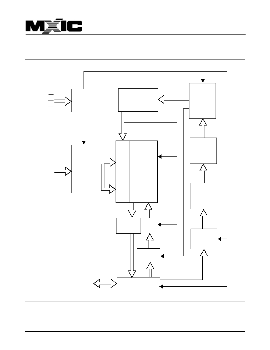
BLOCK DIAGRAM
CONTROL
INPUT
LOGIC
PROGRAM/ERASE
HIGH VOLTAGE
WRITE
STATE
MACHINE
(WSM)
STATE
REGISTER
MX26L6413
FLASH
ARRAY
X-DECODER
ADDRESS
LATCH
AND
BUFFER
Y-PASS GATE
Y
-DECODER
ARRAY
SOURCE
HV
COMMAND
DATA
DECODER
COMMAND
DATA LATCH
I/O BUFFER
PGM
DATA
HV
PROGRAM
DATA LATCH
SENSE
AMPLIFIER
Q0-Q15
A0-A21
CE
OE
WE

5
P/N:PM0914
REV. 0.1, NOV. 20, 2002
MX26L6413
AUTOMATIC PROGRAMMING
The MX26L6413 is word programmable using the Auto-
matic Programming algorithm. The Automatic Program-
ming algorithm makes the external system do not need
to have time out sequence nor to verify the data pro-
grammed. The typical chip programming time at room
temperature of the MX26L6413 is around 140 seconds.
AUTOMATIC PROGRAMMING ALGORITHM
MXIC's Automatic Programming algorithm require the user
to only write program set-up commands (including 2 un-
lock write cycle and A0H) and a program command (pro-
gram data and address). The device automatically times
the programming pulse width, provides the program veri-
fication, and counts the number of sequences. A status
bit similar to DATA polling and a status bit toggling be-
tween consecutive read cycles, provide feedback to the
user as to the status of the programming operation.
AUTOMATIC CHIP ERASE
The entire chip is bulk erased using 50 ms erase pulses
according to MXIC's Automatic Chip Erase algorithm.
Typical erasure at room temperature is around 150 sec-
onds. The Automatic Erase algorithm automatically pro-
grams the entire array prior to electrical erase. The tim-
ing and verification of electrical erase are controlled in-
ternally within the device.
AUTOMATIC ERASE ALGORITHM
MXIC's Automatic Erase algorithm requires the user to
write commands to the command register using stand-
ard microprocessor write timings. The device will auto-
matically pre-program and verify the entire array. Then
the device automatically times the erase pulse width,
provides the erase verification, and counts the number
of sequences. A status bit toggling between consecu-
tive read cycles provides feedback to the user as to the
status of the programming operation.
Register contents serve as inputs to an internal state-
machine which controls the erase and programming cir-
cuitry. During write cycles, the command register inter-
nally latches address and data needed for the program-
ming and erase operations. All address are latched on
the falling edge of WE or CE, whichever happens later.
All data are latched on rising edge of WE or CE, which-
ever happens first.
MXIC's Flash technology combines years of EPROM
experience to produce the highest levels of quality, relia-
bility, and cost effectiveness. The MX26L6413 electri-
cally erases all bits simultaneously using Fowler-Nord-
heim tunneling. The bytes are programmed by using the
EPROM programming mechanism of hot electron injec-
tion.
During a program cycle, the state-machine will control
the program sequences and command register will not
respond to any command set. After the state machine
has completed its task, it will allow the command regis-
ter to respond to its full command set.

6
P/N:PM0914
REV. 0.1, NOV. 20, 2002
MX26L6413
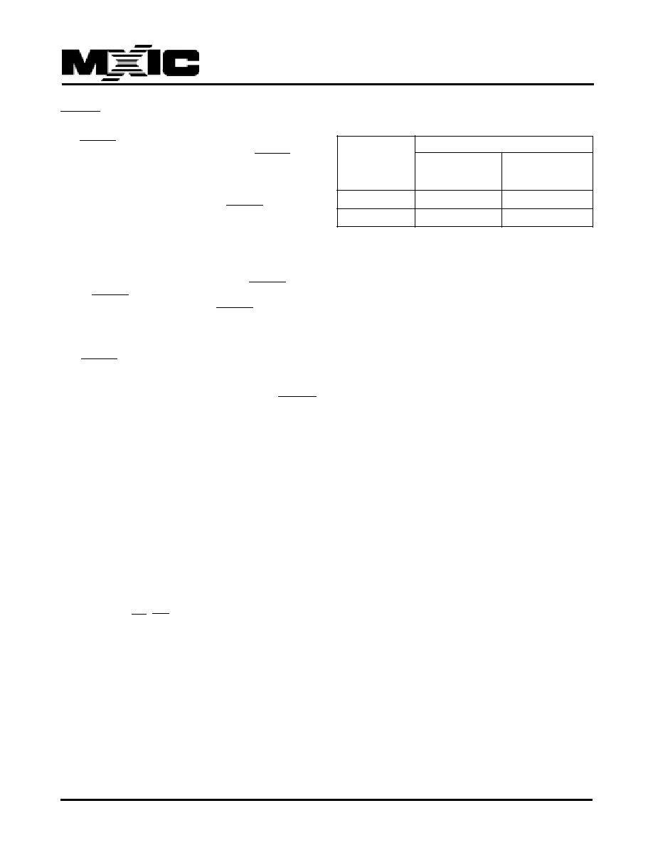
Operation
CE
OE
WE
RESET
Address
Q15~Q0
Read
L
L
H
H
A
IN
D
OUT
Write(Note 1)
L
H
L
H
A
IN
D
IN
Standby
VCC
±
0.3V
X
X
VCC
±
0.3V
X
High-Z
Output Disable
L
H
H
H
X
High-Z
Reset
X
X
X
L
X
High-Z
Legend:
L=Logic LOW=V
IL
,H=Logic High=V
IH
,V
ID
=12.0
±
0.5V,X=Don't Care, A
IN
=Address IN, D
IN
=Data IN, D
OUT
=Data OUT
Notes:
1. When the ACC pin is at V
HH
, the device enters the accelerated program mode. See "Accelerated Program Operations"
for more information.
Table 1
BUS OPERATION(1)
A5
A8
A14
Operation
CE
OE
WE
A0
A1
to
A6
to
A9
to
A15~A21
Q15~Q0
A2
A7
A10
Read Silicon ID
L
L
H
L
L
X
L
X
V
ID
X
X00
C2H
Manufactures Code
Read Silicon ID
L
L
H
H
L
X
L
X
V
ID
X
X
22FCH
Device Code
Secured Silscon
xx88h
Sector Indicator
L
L
H
H
H
X
L
X
V
ID
X
X
(factory locked)
Bit (Q7)
xx08h
(non-factory locked)
Table 2. AUTOSELECT CODES (High Voltage Method)

7
P/N:PM0914
REV. 0.1, NOV. 20, 2002
MX26L6413
REQUIREMENTS FOR READING ARRAY
DATA
To read array data from the outputs, the system must
drive the CE and OE pins to VIL. CE is the power control
and selects the device. OE is the output control and gates
array data to the output pins. WE should remain at VIH.
The internal state machine is set for reading array data
upon device power-up, or after a hardware reset. This
ensures that no spurious alteration of the memory content
occurs during the power transition. No command is
necessary in this mode to obtain array data. Standard
microprocessor read cycles that assert valid address on
the device address inputs produce valid data on the device
data outputs. The device remains enabled for read access
until the command register contents are altered.
WRITE COMMANDS/COMMAND
SEQUENCES
To program data to the device or erase memory , the
system must drive WE and CE to VIL, and OE to VIH.
An erase operation can erase the entire device. The
"Writing specific address and data commands or
sequences into the command register initiates device
operations. Table 1 defines the valid register command
sequences. Writing incorrect address and data values or
writing them in the improper sequence resets the device
to reading array data. Section has details on erasing the
entire chip.
After the system writes the autoselect command
sequence, the device enters the autoselect mode. The
system can then read autoselect codes from the internal
register (which is separate from the memory array) on
Q15-Q0. Standard read cycle timings apply in this mode.
Refer to the Autoselect Mode and Autoselect Command
Sequence section for more information.
ICC2 in the DC Characteristics table represents the active
current specification for the write mode. The "AC
Characteristics" section contains timing specification
table and timing diagrams for write operations.
STANDBY MODE
MX26L6413 can be set into Standby mode with two dif-
ferent approaches. One is using both CE and RESET
pins and the other one is using RESET pin only.
When using both pins of CE and RESET, a CMOS
Standby mode is achieved with both pins held at Vcc ±
0.3V. Under this condition, the current consumed is less
than 50uA (typ.). If both of the CE and RESET are held
at VIH, but not within the range of VCC ±
0.3V, the device
will still be in the standby mode, but the standby current
will be larger. During Auto Algorithm operation, Vcc ac-
tive current (Icc2) is required even CE = "H" until the
operation is completed. The device can be read with stan-
dard access time (tCE) from either of these standby
modes.
When using only RESET, a CMOS standby mode is
achieved with RESET input held at Vss
±
0.3V, Under
this condition the current is consumed less than 50uA
(typ.). Once the RESET pin is taken high. The device is
back to active without recovery delay.
In the standby mode the outputs are in the high imped-
ance state, independent of the OE input.
MX26L6413 is capable to provide the Automatic Standby
Mode to restrain power consumption during read-out of
data. This mode can be used effectively with an applica-
tion requested low power consumption such as handy
terminals.
To active this mode, MX26L6413 automatically switch
themselves to low power mode when MX26L6413 ad-
dresses remain stable during access time of tACC+30ns.
It is not necessary to control CE, WE, and OE on the
mode. Under the mode, the current consumed is typi-
cally 50uA (CMOS level).
OUTPUT DISABLE
With the OE input at a logic high level (VIH), output from
the devices are disabled. This will cause the output pins
to be in a high impedance state.
8
P/N:PM0914
REV. 0.1, NOV. 20, 2002
MX26L6413
RESET OPERATION
The RESET pin provides a hardware method of resetting
the device to reading array data. When the RESET pin is
driven low for at least a period of tRP, the device
immediately terminates any operation in progress, tri-
states all output pins, and ignores all read/write
commands for the duration of the RESET pulse. The
device also resets the internal state machine to reading
array data. The operation that was interrupted should be
reinitiated once the device is ready to accept another
command sequence, to ensure data integrity
Current is reduced for the duration of the RESET pulse.
When RESET is held at VSS
±
0.3V, the device draws
CMOS standby current (ICC4). If RESET is held at VIL
but not within VSS
±
0.3V, the standby current will be
greater.
The RESET pin may be tied to system reset circuitry. A
system reset would that also reset the MTP EPROM.
Refer to the AC Characteristics tables for RESET
parameters and to Figure 14 for the timing diagram.
SILICON ID READ OPERATION
MTP EPROM are intended for use in applications where
the local CPU alters memory contents. As such, manu-
facturer and device codes must be accessible while the
device resides in the target system. EPROM program-
mers typically access signature codes by raising A9 to
a high voltage. However, multiplexing high voltage onto
address lines is not generally desired system design prac-
tice.
MX26L6413 provides hardware method to access the
silicon ID read operation. Which method requires VID on
A9 pin, VIL on CE, OE, A6, and A1 pins. Which apply
VIL on A0 pin, the device will output MXIC's manufac-
ture code of C2H. Which apply VIH on A0 pin, the device
will output MX26L6413 device code of 22FCH.
VI/O PIN OPERATION
MX26L6413 is capable to provide the I/O power supply
(VI/O) pin to control Input/Output voltage levels of the
device. The data outputs and voltage tolerated at its data
input is determined by the voltage on the VI/O pin. This
device is allows to operate in 1.8V or 3V system as re-
quired.
DATA PROTECTION
The MX26L6413 is designed to offer protection against
accidental erasure or programming caused by spurious
system level signals that may exist during power transi-
tion. During power up the device automatically resets
the state machine in the Read mode. In addition, with
its control register architecture, alteration of the memory
contents only occurs after successful completion of spe-
cific command sequences. The device also incorporates
several features to prevent inadvertent write cycles re-
sulting from VCC power-up and power-down transition or
system noise.
SECURED SILICON SECTOR
The MX26L6413 features a Flash memory region where
the system may access through a command sequence
to create a permanent part identification as so called
Electronic Serial Number (ESN) in the device. Once this
region is programmed, any further modification on the
region is impossible. The secured silicon sector is a 512
words in length, and uses a Secured Silicon Sector Indi-
cator Bit (Q7) to indicate whether or not the Secured
Silicon Sector is locked when shipped from the factory.
This bit is permanently set at the factory and cannot be
changed, which prevent duplication of a factory locked
part. This ensures the security of the ESN once the prod-
uct is shipped to the field.
The MX26L6413 offers the device with Secured Silicon
Sector either factory locked or customer lockable. The
factory-locked version is always protected when shipped
from the factory , and has the Secured Silicon Sector
Indicator Bit permanently set to a "1". The customer-
lockable version is shipped with the Secured Silicon
Sector unprotected, allowing customer to utilize that sec-
tor in any form they prefer. The customer-lockable ver-
VCC / VI/O Voltage Range
Part No.
VCC=2.7V to 3.6VVCC=2.7V to 3.6V
VI/O=2.7V to 3.6VVI/O=1.65V to 2.6V
MX26L6413-90
90ns
100ns
MX26L6413-12
120ns
130ns
Table 3
Notes: Typical values measured at VCC=2.7V to 3.6V,
VI/O=2.7V to 3.6V

9
P/N:PM0914
REV. 0.1, NOV. 20, 2002
MX26L6413
sion has the secured sector Indicator Bit permanently
set to a "0". Therefore, the Secured Silicon Sector Indi-
cator Bit permanently set to a "0". Therefore, the Second
Silicon Sector Indicator Bit prevents customer, lockable
device from being used to replace devices that are fac-
tory locked.
The system access the Secured Silicon Sector through
a command sequence (refer to "Enter Secured Silicon/
Exit Secured Silicon Sector command Sequence). After
the system has written the Enter Secured Silicon Sector
command sequence, it may read the Secured Silicon
Sector by using the address normally occupied by the
address 000000h-0001FFh. This mode of operation con-
tinues until the system issues the Exit Secured Silicon
Sector command sequence, or until power is removed
from the device. On power-up, or following a hardware
reset, the device reverts to sending command to ad-
dress 000000h-0001FFFh.
LOW VCC WRITE INHIBIT
When VCC is less than VLKO the device does not ac-
cept any write cycles. This protects data during VCC
power-up and power-down. The command register and
all internal program/erase circuits are disabled, and the
device resets. Subsequent writes are ignored until VCC
is greater than VLKO. The system must provide the proper
signals to the control pins to prevent unintentional write
when VCC is greater than VLKO.
WRITE PULSE "GLITCH" PROTECTION
Noise pulses of less than 5ns(typical) on CE or WE will
not initiate a write cycle.
LOGICAL INHIBIT
Writing is inhibited by holding any one of OE = VIL, CE =
VIH or WE = VIH. To initiate a write cycle CE and WE
must be a logical zero while OE is a logical one.
POWER-UP SEQUENCE
The MX26L6413 powers up in the Read only mode. In
addition, the memory contents may only be altered after
successful completion of the predefined command se-
quences.
FACTORY LOCKED:Secured Silicon Sector
Programmed and Protected At the Factory
In device with an ESN, the Secured Silicon Sector is
protected when the device is shipped from the factory.
The Secured Silicon Sector cannot be modified in any
way. A factory locked device has an 8-word random ESN
at address 000000h-000007h.
CUSTOMER LOCKABLE:Secured Silicon
Sector NOT Programmed or Protected At the
Factory
As an alternative to the factory-locked version, the device
may be ordered such that the customer may program
and protect the 512-word Secured Silicon Sector.
Programming and protecting the Secured Silicon Sector
must be used with caution since, once protected, there
is no procedure available for unprotecting the Secured
Silicon Sector area and none of the bits in the Secured
Silicon Sector memory space can be modified in any
way.
The Secured Silicon Sector area can be protected using
the following procedures:
Write the three-cycle Enter Secured Silicon Sector Region
command sequence. This allows in-system protection
of the Secured Silicon Sector without raising any device
pin to a high voltage. Note that method is only applicable
to the Secured Silicon Sector.
Once the Secured Silicon Sector is programmed, locked
and verified, the system must write the Exit Secured
Silicon Sector Region command sequence to return to
reading and writing the remainder of the array.
10
P/N:PM0914
REV. 0.1, NOV. 20, 2002
MX26L6413
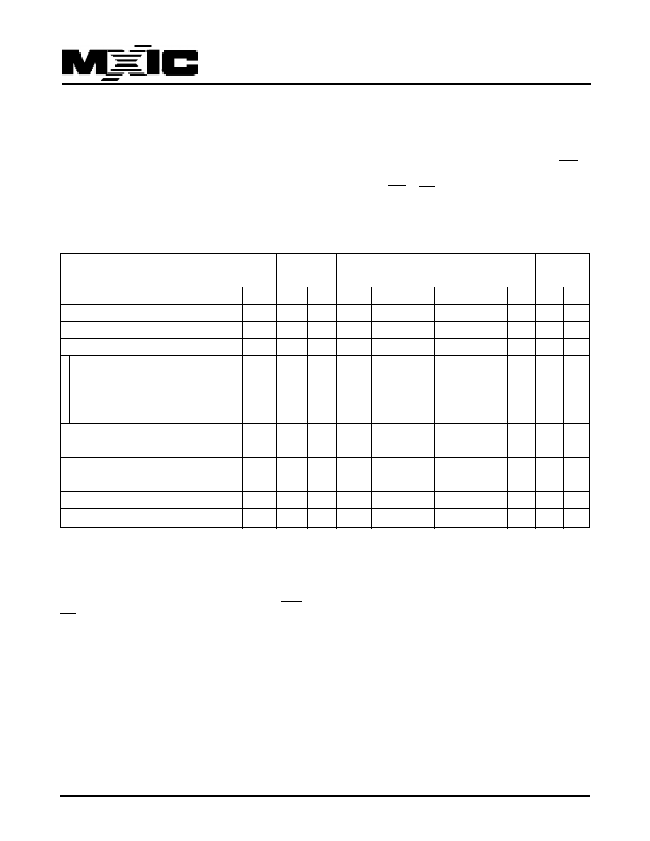
SOFTWARE COMMAND DEFINITIONS
Device operations are selected by writing specific ad-
dress and data sequences into the command register.
Writing incorrect address and data values or writing them
in the improper sequence will reset the device to the
read mode. Table 4 defines the valid register command
sequences. Either of the two reset command sequences
Legend:
X=Don't care
RA=Address of the memory location to be read.
RD=Data read from location RA during read operation.
PA=Address of the memory location to be programmed.
Addresses are latched on the falling edge of the WE or
CE pulse.
PD=Data to be programmed at location PA. Data is
latched on the rising edge of WE or CE pulse.
will reset the device (when applicable).
All addresses are latched on the falling edge of WE or
CE, whichever happens later. All data are latched on ris-
ing edge of WE or CE, whichever happens first.
First Bus
Second Bus Third Bus
Fourth Bus
Fifth Bus
Sixth Bus
Command
Bus
Cycle
Cycle
Cycle
Cycle
Cycle
Cycle
Cycle
Addr
Data
Addr
Data Addr
Data Addr
Data
Addr
Data Addr Data
Read(Note 5)
1
RA
RD
Reset(Note 6)
1
XXX
F0
Autoselect(Note 7)
Manufacturer ID
4
555
AA
2AA
55
555
90
X00
C2
Device ID
4
555
AA
2AA
55
555
90
X01
22FC
Secured Sector
4
555
AA
2AA
55
555
90
x03
see
Factory Protect
Note9
Enter Secured Silicon
3
555
AA
2AA
55
555
88
Sector
Exit Secured Silicon
4
555
AA
2AA
55
555
90
xxx
00
Sector
Porgram
4
555
AA
2AA
55
555
A0
PA
PD
Chip Erase
6
555
AA
2AA
55
555
80
555
AA
2AA
55
555
10
TABLE4. MX26L6413
COMMAND DEFINITIONS
Notes:
1. See Table 1 for descriptions of bus operations.
2. All values are in hexadecimal.
3. Except when reading array or autoselect data, all bus cycles are write operation.
4. Address bits are don't care for unlock and command cycles, except when PA is required.
5. No unlock or command cycles required when device is in read mode.
6. The Reset command is required to return to the read mode when the device is in the autoselect mode or if Q5 goes
high.
7. The fourth cycle of the autoselect command sequence is a read cycle.
8. In the third and fourth cycles of the command sequence, set A21=0.
9. Command is valid when device is ready to read array data or when device is in autoselect mode.
10. The data is 88h for factory locked and 08h for non-factory locked.

11
P/N:PM0914
REV. 0.1, NOV. 20, 2002
MX26L6413
READING ARRAY DATA
The device is automatically set to reading array data
after device power-up. No commands are required to
retrieve data. The device is also ready to read array data
after completing an Automatic Program or Automatic
Erase algorithm.
The system
must
issue the reset command to re-en-
able the device for reading array data if Q5 goes high, or
while in the autoselect mode. See the "Reset Command"
section, next.
RESET COMMAND
Writing the reset command to the device resets the
device to reading array data. Address bits are don't care
for this command.
The reset command may be written between the se-
quence cycles in an erase command sequence before
erasing begins. This resets the device to reading array
data. Once erasure begins, however, the device ignores
reset commands until the operation is complete.
The reset command may be written between the se-
quence cycles in a program command sequence before
programming begins. This resets the device to reading
array data. Once programming begins, however, the
device ignores reset commands until the operation is
complete.
The reset command may be written between the se-
quence cycles in an SILICON ID READ command
sequence. Once in the SILICON ID READ mode, the
reset command
must
be written to return to reading array
data.
If Q5 goes high during a program or erase operation,
writing the reset command returns the device to reading
array data.
SILICON ID READ COMMAND SEQUENCE
The SILICON ID READ command sequence allows the
host system to access the manufacturer and devices
codes, and determine whether or not. Table 4 shows the
address and data requirements. This method is an
alternative to that shown in Table 1, which is intended for
EPROM programmers and requires V
ID
on address bit
A9.
The SILICON ID READ command sequence is initiated
by writing two unlock cycles, followed by the SILICON
ID READ command. The device then enters the SILICON
ID READ mode, and the system may read at any address
any number of times, without initiating another command
sequence. A read cycle at address XX00h retrieves the
manufacturer code. A read cycle at address XX01h re-
turns the device code.
The system must write the reset command to exit the
autoselect mode and return to reading array data.
WORD PROGRAM COMMAND SEQUENCE
The command sequence requires four bus cycles, and
is initiated by writing two unlock write cycles, followed
by the program set-up command. The program address
and data are written next, which in turn initiate the
Embedded Program algorithm. The system is
not
required
to provide fur ther controls or timings. The device
automatically generates the program pulses and verifies
the programmed cell margin. Table 4 shows the address
and data requirements for the byte program command
sequence.
When the Embedded Program algorithm is complete, the
device then returns to reading array data and addresses
are no longer latched. The system can determine the
status of the program operation by using Q7, Q6. See
"Write Operation Status" for information on these status
bits.
Any commands written to the device during the Em-
bedded Program Algorithm are ignored. Note that a
hardware reset immediately terminates the programming
operation. The Word Program command sequence should
be reinitiated once the device has reset to reading array
data, to ensure data integrity.
Programming is allowed in any sequence. A bit cannot
be programmed from a "0" back to a "1". Cause the Data
Polling algorithm to indicate the operation was successful.
However, a succeeding read will show that the data is
still "0". Only erase operations can convert a "0" to a
"1".

12
P/N:PM0914
REV. 0.1, NOV. 20, 2002
MX26L6413
ACCELERATED PROGRAM OPERATIONS
The device offers accelerated program operations through
the ACC pin. When the system asserts V
HH
on the ACC
pin, the device automatically bypass the two "Unlock"
write cycle. The device uses the higher voltage on the
ACC pin to accelerate the operation. Removing V
HH
from
the ACC pin returns the device to normal operation. Under
normal operation ACC can be VCC or GND. Note that the
ACC pin must not be at V
HH
any operation other than
accelerated programming, or device damage may result.
SETUP AUTOMATIC CHIP ERASE
Chip erase is a six-bus cycle operation. There are two
"unlock" write cycles. These are followed by writing the
"set-up" command 80H. Two more "unlock" write cycles
are then followed by the chip erase command 10H.
The MX26L6413 contains a Silicon-ID-Read operation to
supplement traditional PROM programming methodology.
The operation is initiated by writing the read silicon ID
command sequence into the command register. Follow-
ing the command write, a read cycle with A6=VIL,
A1=VIL, A0=VIL retrieves the manufacturer code of C2H.
A read cycle with A6=VIL, A1=VIL, A0=VIH returns the
device code of 22FCH for MX26L6413.
AUTOMATIC CHIP ERASE COMMAND
The device does not require the system to preprogram
prior to erase. The Automatic Erase algorithm automati-
cally preprogram and verifies the entire memory for an
all zero data pattern prior to electrical erase. The system
is not required to provide any controls or timings during
these operations. Table 4 shows the address and data
requirements for the chip erase command sequence.
Any commands written to the chip during the Automatic
Erase algorithm are ignored. Note that a hardware reset
during the chip erase operation immediately terminates
the operation. The Chip Erase command sequence should
be reinitiated once the device has returned to reading
array data, to ensure data integrity.
The system can determine the status of the erase op-
eration by using Q7, Q6. See "Write Operation Status"
for information on these status bits. When the Automatic
Erase algorithm is complete, the device returns to read-
ing array data and addresses are no longer latched.
Figure 5 illustrates the algorithm for the erase opera-tion.
See the Erase/Program Operations tables in "AC Char-
acteristics" for parameters, and to Figure 4 for timing
diagrams.
TABLE 5. SILICON ID CODE
Pins
A0
A1
A6
Q15
Q7
Q6
Q5
Q4
Q3
Q2
Q1
Q0
Code(Hex)
|
Q8
Manufacture code
VIL
VIL
VIL
00H
1
1
0
0
0
0
1
0
00C2H
Device code for MX26L6413 VIH VIL
VIL
22H
1
1
1
1
1
1
1
0
22FCH

13
P/N:PM0914
REV. 0.1, NOV. 20, 2002
MX26L6413
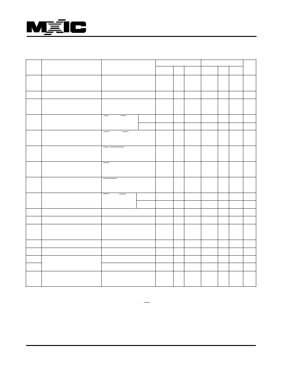
WRITE OPERATION STATUS
The device provides several bits to determine the status
of a write operation: Q5, Q6, Q7. Table 10 and the follow-
ing subsections describe the functions of these bits. Q7,
and Q6 each offer a method for determining whether a
program or erase operation is complete or in progress.
These three bits are discussed first.
Table 6. Write Operation Status
Notes:
1. Performing successive read operations from any address will cause Q6 to toggle.
Status
Q7
Q6
Q5
Note1
In Progress Word Program in Auto Program Algorithm
Q7
Toggle
0
Auto Erase Algorithm
0
Toggle
0
Exceeded
Word Program in Auto Program Algorithm
Q7
Toggle
1
Time Limits Auto Erase Algorithm
0
Toggle
1

14
P/N:PM0914
REV. 0.1, NOV. 20, 2002
MX26L6413
Q7: Data Polling
The Data Polling bit, Q7, indicates to the host system
whether an Automatic Algorithm is in progress or com-
pleted. Data Polling is valid after the rising edge of the
final WE pulse in the program or erase command se-
quence.
During the Automatic Program algorithm, the device out-
puts on Q7 the complement of the datum programmed
to Q7. This Q7 status also applies to programming dur-
ing Erase Suspend. When the Automatic Program algo-
rithm is complete, the device outputs the datum pro-
grammed to Q7. The system must provide the program
address to read valid status information on Q7.
During the Automatic Erase algorithm, Data Polling pro-
duces a "0" on Q7. When the Automatic Erase algo-
rithm is complete. Data Polling produces a "1" on Q7.
This is analogous to the complement/true datum output
described for the Automatic Program algorithm: the erase
function changes all the bits to "1" prior to this, the de-
vice outputs the "complement," or "0".
After an erase command sequence is written, if all sec-
tors selected for erasing are protected, Data Polling on
Q7 is active for approximately 100 us, then the device
returns to reading array data.
When the system detects Q7 has changed from the
complement to true data, it can read valid data at Q7-Q0
on the following read cycles. This is because Q7 may
change asynchronously with Q0-Q6 while Output Enable
(OE) is asserted low.
Q6:Toggle BIT I
Toggle Bit I on Q6 indicates whether an Automatic Pro-
gram or Erase algorithm is in progress or complete. Toggle
Bit I may be read at any address, and is valid after the
rising edge of the final WE or CE, whichever happens
first pulse in the command sequence (prior to the pro-
gram or erase operation).
During an Automatic Program or Erase algorithm opera-
tion, successive read cycles to any address cause Q6
to toggle. The system may use either OE or CE to con-
trol the read cycles. When the operation is complete, Q6
stops toggling.
Table 6 shows the outputs for Toggle Bit I on Q6.
Q5:Program/Erase Timing
Q5 will indicate if the program or erase time has exceeded
the specified limits (internal pulse count). Under these
conditions Q5 will produce a "1". This time-out condition
indicates that the program or erase cycle was not suc-
cessfully completed. Data Polling and Toggle Bit are the
only operating functions of the device under this condi-
tion.
If this time-out condition occurs during chip erase opera-
tion, it specifies that device is bad and it may not be
reused. Write the Reset command sequence to the de-
vice, and then execute program or erase command se-
quence. This allows the system to continue to use the
other active sectors in the device.
If this time-out condition occurs during the chip erase
operation, it specifies that the entire chip is bad.
If this time-out condition occurs during the word program-
ming operation, the word is bad and may not be reused,
(other word are still functional and can be reused).

15
P/N:PM0914
REV. 0.1, NOV. 20, 2002
MX26L6413
ABSOLUTE MAXIMUM RATINGS
Storage Temperature
Plastic Packages . . . . . . . . . . . . . ..... -65
o
C to +150
o
C
Ambient Temperature
with Power Applied. . . . . . . . . . . . . .... -65
o
C to +125
o
C
Voltage with Respect to Ground
VCC (Note 1) . . . . . . . . . . . . . . . . . -0.5 V to +4.0 V
A9, OE, and
RESET (Note 2) . . . . . . . . . . . ....-0.5 V to +12.5 V
All other pins (Note 1) . . . . . . . -0.5 V to VCC +0.5 V
Output Short Circuit Current (Note 3) . . . . . . 200 mA
Notes:
1. Minimum DC voltage on input or I/O pins is -0.5 V.
During voltage transitions, input or I/O pins may over-
shoot VSS to -2.0 V for periods of up to 20 ns. See
Figure 6. Maximum DC voltage on input or I/O pins is
VCC +0.5 V. During voltage transitions, input or I/O
pins may overshoot to VCC +2.0 V for periods up to
20 ns. See Figure 7.
2. Minimum DC input voltage on pins A9, OE, and
RESET is -0.5 V. During voltage transitions, A9, OE,
and RESET may overshoot VSS to -2.0 V for periods
of up to 20 ns. See Figure 6. Maximum DC input volt-
age on pin A9 is +12.5 V which may overshoot to 14.0
V for periods up to 20 ns.
3. No more than one output may be shorted to ground at
a time. Duration of the short circuit should not be
greater than one second.
Stresses above those listed under "Absolute Maximum
Ratings" may cause permanent damage to the device.
This is a stress rating only; functional operation of the
device at these or any other conditions above those in-
dicated in the operational sections of this data sheet is
not implied. Exposure of the device to absolute maxi-
mum rating conditions for extended periods may affect
device reliability.
OPERATING RATINGS
Commercial (C) Devices
Ambient Temperature (T
A
). . . . . . . . . . . . 0
∞
C to +70
∞
C
Industrial (I) Devices
Ambient Temperature (T
A
). . . . . . . . . . -40
∞
C to +85
∞
C
V
CC
Supply Voltages
V
CC
for full voltage range . . . . . . . . . . . . +2.7 V to 3.6 V
Operating ranges define those limits between which the
functionality of the device is guaranteed.
16
P/N:PM0914
REV. 0.1, NOV. 20, 2002
MX26L6413
Para-
VI/O=2.7V~3.6V
VI/O=1.65V~2.6V
meter Description
Test Conditions
Min
Typ
Max
Min
Typ
Max
Unit
I LI
Input Load Current (Note 1)
VIN = VSS to VCC ,
±
1.0
±
1.0
uA
VCC = VCC max
I LIT
A9 Input Load Current
VCC=VCC max; A9 = 12.5V
35
35
uA
I LO
Output Leakage Current
VOUT = VSS to VCC ,
±
1.0
±
1.0
uA
VCC= VCC max
ICC1
VCC Active Read Current
CE= VIL, OE = VIH 5 MHz
17
25
17
25
mA
(Notes1, 2)
1 MHz
4
7
4
7
mA
ICC2
VCC Active Write Current
CE= V IL , OE = V IH
26
30
26
30
mA
(Notes 1, 3, 4)
ICC3
VCC Standby Current (CMOS) CE,RESET,
30
100
30
100
uA
(Note 1)
ACC=VCC
±
0.3V
ICC4
VCC Standby Current (TTL)
CE=VIH
0.5
1
0.5
1
mA
(Note 1)
ICC5
VCC Reset Current (Note 1)
RESET = V SS
±
0.3 V,
0.2
5
0.2
5
uA
ACC = VCC
±
0.3 V
IACC
ACC Accelerated Program
CE=VIL, OE=VIH
Acc pin
5
10
5
10
mA
Current, Word
Vcc pin
15
30
15
30
mA
VIL
Input Low Voltage
-0.5
0.8
0.4
V
VIH
Input High Voltage
0.7xVcc
Vcc+0.3 VI/O-0.4
V
VHH
Voltage for ACC
VCC = 3.0 V
±
10%
11.5
12.5
11.5
12.5
V
Program Acceleration
VID
Voltage for Autoselect
VCC = 3.0 V
±
10%
11.5
12.5
11.5
12.5
V
VOL
Output Low Voltage
IOL= 4.0mA,VCC=VCC min
0.45
0.45
V
VOH1 Output High Voltage
IOH=-2.0mA,VCC=VCC min 0.85VI/O
0.85VI/O
V
VOH2
IOH=-100uA,VCC=VCC min VI/O-0.4
VI/O-0.4
V
VLKO Low V CC Lock-Out Voltage
2.3
2.5
2.3
2.5
V
(Note 4)
Notes:
1. Maximum ICC specifications are tested with VCC = VCC max.
2. The ICC current listed is typically is less than 2 mA/MHz, with OE at V IH . Typical specifications are for VCC = 3.0 V.
3. ICC active while Embedded Erase or Embedded Program is in progress.
4. Not 100% tested.
DC CHARACTERISTICS TA=0
∞
∞
∞
∞
∞
C to 70
∞
∞
∞
∞
∞
C, VCC=2.7V~3.6V
17
P/N:PM0914
REV. 0.1, NOV. 20, 2002
MX26L6413
SWITCHING TEST CIRCUITS
WAVEFORM
INPUTS
OUTPUTS
Steady
Changing from H to L
Changing from L to H
Don't Care, Any Change Permitted
Changing, State Unknown
Does Not Apply
Center Line is High Impedance State (High Z)
KEY TO SWITCHING WAVEFORMS
SWITCHING TEST WAVEFORMS
TEST SPECIFICATIONS
Test Condition
90ns 120ns
Unit
Output Load
1 TTL gate
Output Load Capacitance,
30 100
pF
CL (including jig capacitance)
Input Rise and Fall Times
5
ns
Input Pulse Levels
0.0-3.0
V
Input timing measurement
1.5
V
reference levels
Output timing measurement
1.5
V
reference levels
DEVICE UNDER
TEST
DIODES=IN3064
OR EQUIVALENT
CL
6.2K ohm
2.7K ohm
3.3V
1.5V
VIO/2
Measurement Level
3.0V
0.0V
OUTPUT
INPUT
18
P/N:PM0914
REV. 0.1, NOV. 20, 2002
MX26L6413
Symbol
DESCRIPTION
CONDITION
90ns
120ns
Unit
tACC
Address to output delay
CE=VIL MAX
90
120
ns
OE=VIL
tCE
Chip enable to output delay
OE=VIL MAX
90
120
ns
tOE
Output enable to output delay
MAX
34
44
ns
tDF
OE High to output float(Note1)
MAX
25
35
ns
tOH
Output hold time of from the rising edge of
MIN
0
0
ns
Address, CE, or OE, whichever happens first
tRC
Read cycle time (Note 1)
MIN
90
120
ns
tWC
Write cycle time (Note 1)
MIN
90
120
ns
tCWC
Command write cycle time(Note 1)
MIN
90
120
ns
tAS
Address setup time
MIN
0
0
ns
tAH
Address hold time
MIN
45
50
ns
tDS
Data setup time
MIN
45
50
ns
tDH
Data hold time
MIN
0
0
ns
tVCS
Vcc setup time(Note 1)
MIN
50
50
us
tCS
Chip enable setup time
MIN
0
0
ns
tCH
Chip enable hold time
MIN
0
0
ns
tOES
Output enable setup time (Note 1)
MIN
0
0
ns
tOEH
Output enable hold time (Note 1)
Read
MIN
0
0
ns
Toggle &
MIN
10
10
ns
Data Polling
tWES
WE setup time
MIN
0
0
ns
tWEH
WE hold time
MIN
0
0
ns
tCEP
CE pulse width
MIN
45
50
ns
tCEPH
CE pulse width high
MIN
30
30
ns
tWP
WE pulse width
MIN
35
50
ns
tWPH
WE pulse width high
MIN
30
30
ns
tOLZ
Output enable to output low Z
MAX
30
40
ns
tWHGL
WE high to OE going low
MIN
30
30
ns
tWHWH1 Word Programming Operation (Note 3)
TYP
11
11
us
tWHWH1 Accelerated Word Programming Operation(Note3)
TYP
7
7
us
tWHWH2 Chip Erase Operation (Note3)
TYP
150
150
sec
Note:
1.Not 100% Tested
2.t
r
= t
f
= 5ns
3. See the " Erase and Program Performance" section for more information.
AC CHARACTERISTICS TA=0
∞
∞
∞
∞
∞
C to 70
∞
∞
∞
∞
∞
C, VCC=2.7V~3.6V
19
P/N:PM0914
REV. 0.1, NOV. 20, 2002
MX26L6413
Fig 1. COMMAND WRITE OPERATION
READ/RESET OPERATION
Fig 2. READ TIMING WAVEFORMS
Addresses
CE
OE
tACC
WE
VIH
VIL
VIH
VIL
VIH
VIL
VIH
VIL
VOH
VOL
HIGH Z
HIGH Z
DATA Valid
tOE
tOLZ
tOEH
tDF
tCE
tRC
Outputs
tOH
ADD Valid
Addresses
CE
OE
WE
DIN
tDS
tAH
Data
tDH
tCS
tCH
tCWC
tCEPH1
tCEP
tOES
tAS
VCC
3V
VIH
VIL
VIH
VIL
VIH
VIL
VIH
VIL
VIH
VIL
ADD Valid
20
P/N:PM0914
REV. 0.1, NOV. 20, 2002
MX26L6413
Fig 3. RESET TIMING WAVEFORM
AC CHARACTERISTICS TA=0
∞
∞
∞
∞
∞
C to 70
∞
∞
∞
∞
∞
C, VCC=2.7V~3.6V
Parameter
Description
Test Setup
All Speed Options Unit
tREADY
RESET PIN Low (NOT During Automatic
MAX
500
ns
Algorithms) to Read or Write (See Note)
tRP1
RESET Pulse Width (During Automatic Algorithms)
MIN
10
us
tRP2
RESET Pulse Width (NOT During Automatic Algorithms)
MIN
500
ns
tRH
RESET High Time Before Read (See Note)
MIN
50
ns
Note:Not 100% tested
tRH
tRP2
tRP1
tReady
CE, OE
RESET
Reset Timing NOT during Automatic Algorithms
Reset Timing during Automatic Algorithms
RESET
21
P/N:PM0914
REV. 0.1, NOV. 20, 2002
MX26L6413
ERASE/PROGRAM OPERATION
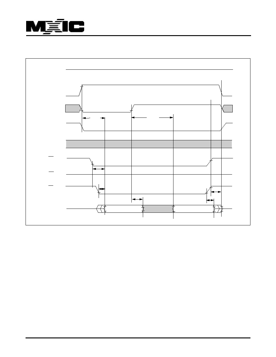
Fig 4. AUTOMATIC CHIP ERASE TIMING WAVEFORM
tWC
Address
OE
CE
55h
2AAh
555h
10h
In
Progress Complete
VA
VA
tAS
tAH
tGHWL
tCH
tWHGL
tWP
tDS tDH
tWHWH2
Read Status Data
Erase Command Sequence(last two cycle)
tCS
tWPH
tVCS
WE
Data
VCC

22
P/N:PM0914
REV. 0.1, NOV. 20, 2002
MX26L6413
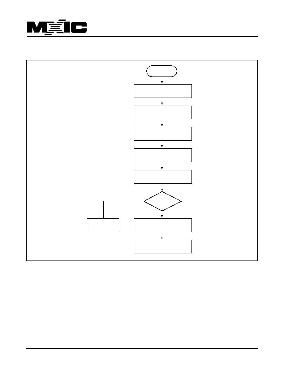
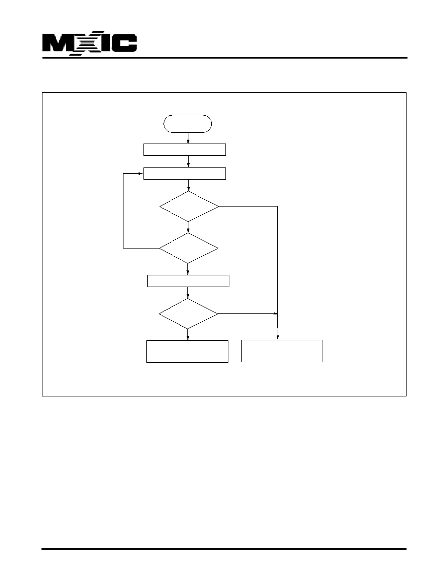
Fig 5. AUTOMATIC CHIP ERASE ALGORITHM FLOWCHART
START
Write Data AAH Address 555H
Write Data 55H Address 2AAH
Write Data AAH Address 555H
Write Data 80H Address 555H
YES
Write Data 10H Address 555H
Write Data 55H Address 2AAH
DATA = FFh ?
YES
Auto Erase Completed
Data Poll
from system
No
23
P/N:PM0914
REV. 0.1, NOV. 20, 2002
MX26L6413
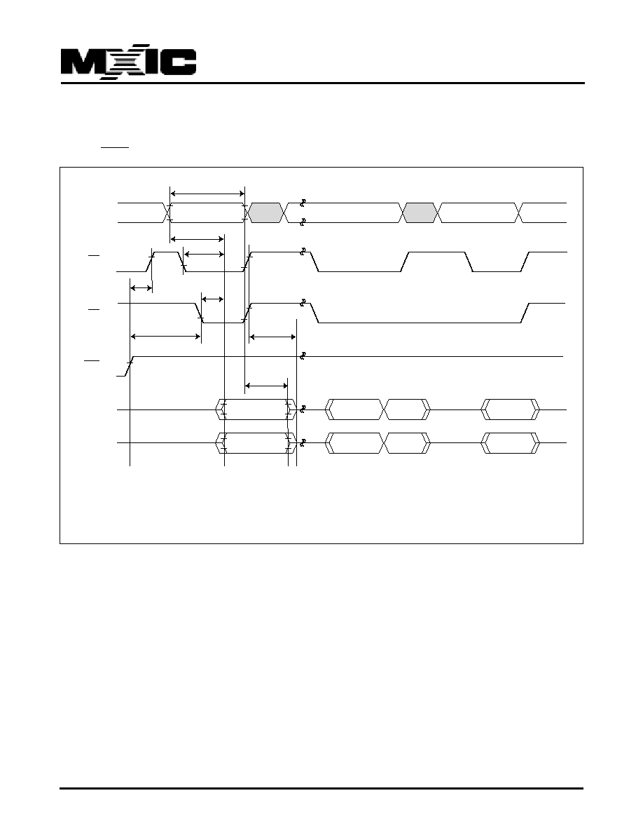
Fig 6. AUTOMATIC PROGRAM TIMING WAVEFORMS
Fig 7. Accelerated Program Timing Diagram
ACC
tVHH
VHH
(8.5V ~ 9.5V)
VIL or VIH
VIL or VIH
tVHH
tWC
Address
OE
CE
A0h
555h
PA
PD
Status
DOUT
PA
PA
NOTES:
1. PA=Program Address, PD=Program Data, DOUT is the true data the program address
tAS
tAH
tGHWL
tCH
tWP
tDS
tDH
tWHWH1
Read Status Data (last two cycle)
Program Command Sequence(last two cycle)
tWHGL
tCS
tWPH
tVCS
WE
Data
VCC
24
P/N:PM0914
REV. 0.1, NOV. 20, 2002
MX26L6413
Fig 8. CE CONTROLLED PROGRAM TIMING WAVEFORM
tWC
tWH
tGHEL
tWHWH1 or 2
tCP
Address
WE
OE
CE
Data
DQ7
PA
Data Polling
DOUT
RESET
NOTES:
1. PA=Program Address, PD=Program Data, DOUT=Data Out, DQ7=complement of data written to device.
2. Figure indicates the last two bus cycles of the command sequence.
tAH
tAS
PA for program
555 for chip erase
tWHGL
tRH
tDH
tDS
tWS
A0 for program
55 for erase
tCPH
tBUSY
PD for program
10 for chip erase
555 for program
2AA for erase
25
P/N:PM0914
REV. 0.1, NOV. 20, 2002
MX26L6413
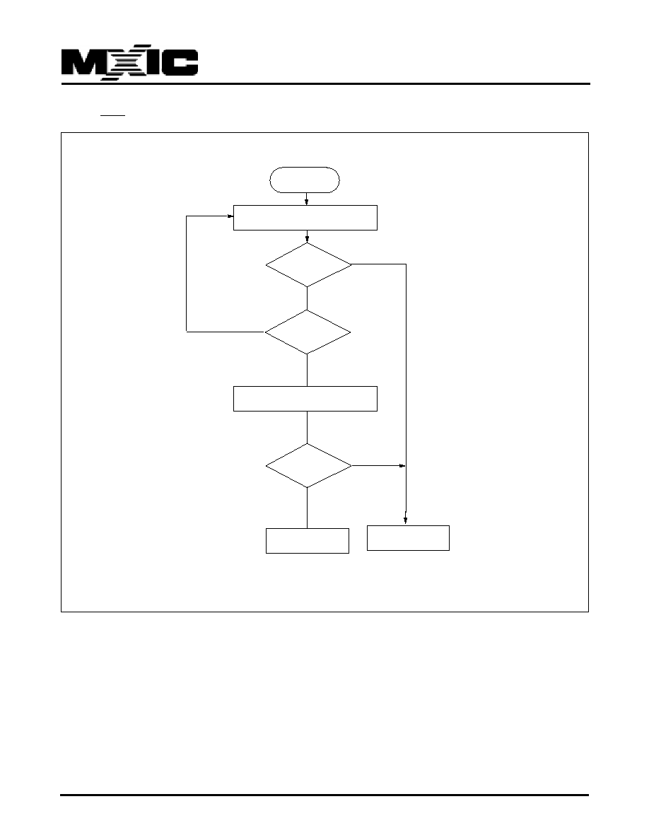
Fig 9. AUTOMATIC PROGRAMMING ALGORITHM FLOWCHART
START
Write Data AAH Address 555H
Write Data 55H Address 2AAH
Write Program Data/Address
Write Data A0H Address 555H
YES
Verify Word Ok ?
YES
Auto Program Completed
Data Poll
from system
Increment
Address
Last Address ?
No
No
26
P/N:PM0914
REV. 0.1, NOV. 20, 2002
MX26L6413
Fig 10. SECURED SILICON SECTOR PROTECTED ALGORITHMS FLOWCHART
START
Enter Secured Silicon Sector
Wait 1us
Second Wait Cycle Data=60h
A6=0, A1=1, A0=0
Frist Wait Cycle Data=60h
YES
NO
Data=01h?
Wait 300us
Write Reset Command
Device Failed
Secured Sector Protect Complete
27
P/N:PM0914
REV. 0.1, NOV. 20, 2002
MX26L6413
Fig 11. SILICON ID READ TIMING WAVEFORM
tACC
tCE
tACC
tOE
tOH
tOH
tDF
DATA OUT
00C2H
22FC
VID
VIH
VIL
ADD
A9
ADD
CE
A1
OE
WE
ADD
A0
DATA OUT
DATA
Q0-Q15
VCC
3V
VIH
VIL
VIH
VIL
VIH
VIL
VIH
VIL
VIH
VIL
VIH
VIL
VIH
VIL
28
P/N:PM0914
REV. 0.1, NOV. 20, 2002
MX26L6413
WRITE OPERATION STATUS
Fig 12. DATA POLLING TIMING WAVEFORMS (DURING AUTOMATIC ALGORITHMS)
NOTES:
VA=Valid address. Figure shows are first status cycle after command sequence, last status read cycle, and array data read cycle.
tDF
tCE
tACC
tRC
tCH
tOE
tOEH
tOH
Address
CE
OE
WE
Q7
Q0-Q6
Status Data
Status Data
Complement
Complement
Valid Data
True
VA
VA
VA
High Z
High Z
Valid Data
True
29
P/N:PM0914
REV. 0.1, NOV. 20, 2002
MX26L6413
Fig 13. Data Polling Algorithm
START
Read Q7~Q0
Add. = VA (1)
Yes
Yes
Yes
No
No
No
Q7 = Data ?
Q7 = Data ?
Q5 = 1 ?
Read Q7~Q0
Add. = VA
PASS
FAIL
(2)
Notes:
1.VA=valid address for programming.
2.Q7 should be rechecked even Q5="1"because Q7 may change simultaneously with Q5.

30
P/N:PM0914
REV. 0.1, NOV. 20, 2002
MX26L6413
Fig 14. TOGGLE BIT TIMING WAVEFORMS (DURING AUTOMATIC ALGORITHMS)
NOTES:
VA=Valid address; not required for Q6. Figure shows first two status cycle after command sequence, last status read cycle, and
array data read cycle.
tDF
tCE
tACC
tRC
tCH
tOE
tOEH
High Z
tOH
Address
CE
OE
WE
Q6
Valid Status
(first raed)
Valid Status
(second read)
(stops toggling)
Valid Data
VA
VA
VA
VA
Valid Data
31
P/N:PM0914
REV. 0.1, NOV. 20, 2002
MX26L6413
START
Read Q7~Q0
Read Q7~Q0
YES
NO
Toggle Bit Q6
=Toggle?
Q5=1?
YES
NO
(Note 1)
Read Q7~Q0 Twice
(Note 1,2)
Toggle Bit Q6=
Toggle?
Program/Erase Operation Not
Complete, Write Reset Command
YES
Program/Erase Operation Complete
Fig 15. Toggle Bit Algorithm
Note:
1.Read toggle bit twice to determine whether or not it is toggling.
2.Recheck toggle bit because it may stop toggling as Q5 changes to "1".
32
P/N:PM0914
REV. 0.1, NOV. 20, 2002
MX26L6413
MIN.
MAX.
Input Voltage with respect to GND on all pins except I/O pins
-1.0V
13.5V
Input Voltage with respect to GND on all I/O pins
-1.0V
Vcc + 1.0V
Current
-100mA
+100mA
Includes all pins except Vcc. Test conditions: Vcc = 5.0V, one pin at a time.
LIMITS
PARAMETER
MIN.
TYP.(2)
MAX.
UNITS
Chip Erase Time
150
300
sec
Word Programming Time
30
350
us
Chip Programming Time
140
250
sec
Accelerated Chip Erase Time
75
150
sec
Accelerated Word Program Time
7
210
us
Accelerated Chip Program Time
70
125
sec
Erase/Program Cycles
100
Cycles
LATCH-UP CHARACTERISTICS
ERASE AND PROGRAMMING PERFORMANCE(1)
Note:
1. Not 100% Tested, Excludes external system level over head.
2. Typical values measured at 25
∞
C,3.3V. Additionally programming typically assume checkerboard pattern.
Parameter Symbol
Parameter Description
Test Set
TYP
MAX
UNIT
CIN
Input Capacitance
VIN=0
6
7.5
pF
COUT
Output Capacitance
VOUT=0
8.5
12
pF
CIN2
Control Pin Capacitance
VIN=0
7.5
9
pF
CAPACITANCE TA=0
∞
∞
∞
∞
∞
C to 70
∞
∞
∞
∞
∞
C, VCC=2.7V~3.6V
Notes:
1. Sampled, not 100% tested.
2. Test conditions TA=25
∞
C, f=1.0MHz
Parameter
Test Conditions
Min
Unit
Minimum Pattern Data Retention Time
150
10
Years
125
20
Years
DATA RETENTION

33
P/N:PM0914
REV. 0.1, NOV. 20, 2002
MX26L6413
ORDERING INFORMATION
PLASTIC PACKAGE
PART NO.
ACCESS TIME
Temperature
Package type
Ball Pitch
(ns)
Range
MX26L6413TC-90
90
Commerical
48 pin TSOP
(Normal Type)
MX26L6413TC-12
120
Commerical
48 pin TSOP
(Normal Type)
MX26L6413XBC-90
90
Commerical
48 ball CSP
0.8 mm
MX26L6413XBC-12
120
Commerical
48 ball CSP
0.8 mm
MX26L6413TI-90
90
Industrial
48 pin TSOP
(Normal Type)
MX26L6413TI-12
120
Industrial
48 pin TSOP
(Normal Type)
MX26L6413XBI-90
90
Industrial
48 ball CSP
0.8 mm
MX26L6413XBI-12
120
Industrial
48 ball CSP
0.8 mm
34
P/N:PM0914
REV. 0.1, NOV. 20, 2002
MX26L6413
PACKAGE INFORMATION
35
P/N:PM0914
REV. 0.1, NOV. 20, 2002
MX26L6413

36
P/N:PM0914
REV. 0.1, NOV. 20, 2002
MX26L6413
REVISION HISTORY
Revision No. Description
Page
Date
0.1
1. To modify Package Information
P34,35
NOV/20/2002

MX26L6413
M
ACRONIX
I
NTERNATIONAL
C
O.,
L
TD.
HEADQUARTERS:
TEL:+886-3-578-6688
FAX:+886-3-563-2888
EUROPE OFFICE:
TEL:+32-2-456-8020
FAX:+32-2-456-8021
JAPAN OFFICE:
TEL:+81-44-246-9100
FAX:+81-44-246-9105
SINGAPORE OFFICE:
TEL:+65-348-8385
FAX:+65-348-8096
TAIPEI OFFICE:
TEL:+886-2-2509-3300
FAX:+886-2-2509-2200
M
ACRONIX
A
MERICA,
I
NC.
TEL:+1-408-453-8088
FAX:+1-408-453-8488
CHICAGO OFFICE:
TEL:+1-847-963-1900
FAX:+1-847-963-1909
http : //www.macronix.com
MACRONIX INTERNATIONAL CO., LTD. reserves the right to change product and specifications without notice.