
FEATURES
∑ 131,072 bytes by 8-bit organization
∑ Fast access time: 70ns(Vcc:5V
±
5%; CL:35pF)
90/120ns(Vcc:5V
±
10%; CL:100pF)
∑ Low power consumption
≠ 50mA maximum active current
≠ 100uA maximum standby current
∑ Programming and erasing voltage 12V
±
5%
∑ Command register architecture
≠ Byte Programming (15us typical)
≠ Auto chip erase 5 seconds typical
(including preprogramming time)
≠ Block Erase
∑ Optimized high density blocked architecture
≠ Four 4-KB blocks
1
P/N: PM0340
REV. 1.6,JAN. 19, 1999
GENERAL DESCRIPTION
The MX28F1000P is a 1-mega bit Flash memory or-
ganized as 128K bytes of 8 bits each. MXIC's Flash
memories offer the most cost-effective and reliable
read/write non-volatile random access memory. The
MX28F1000P is packaged in 32-pin PDIP, PLCC
and TSOP. It is designed to be reprogrammed and
erased in-system or in-standard EPROM program-
mers.
The standard MX28F1000P offers access times as
fast as 70 ns, allowing operation of high-speed
microprocessors without wait states. To eliminate
bus contention, the MX28F1000P has separate chip
enable (CE) and output enable (OE ) controls.
MXIC's Flash memories augment EPROM function-
a l i t y w i t h i n - c i r c u i t e l e c t r i c a l e r a s u r e a n d
programming. The MX28F1000P uses a command
r e g i s t e r t o m a n a g e t h i s f u n c t i o n a l i t y , w h i l e
m a i n t a i n i n g a s t a n d a r d 3 2 - p i n p i n o u t . T h e
command register allows for 100% TTL level control
inputs and fixed power supply levels during erase
and programming, while maintaining maximum
EPROM compatibility.
MXIC Flash technology reliably stores memory con-
tents even after 10,000 erase and program cycles.
The MXIC cell is designed to optimize the erase and
programming mechanisms. In addition, the combi-
nation of advanced tunnel oxide processing and low
internal electric fields for erase and programming
o p e r a t i o n s p r o d u c e s r e l i a b l e c y c l i n g . T h e
MX28F1000P uses a 12.0V
±
5% VPP supply to
perform the Auto Program/Erase algorithms.
The highest degree of latch-up protection is
achieved with MXIC's proprietary non-epi process.
Latch-up protection is proved for stresses up to 100
milliamps on address and data pin from -1V to VCC
+ 1V.
≠ Seven 16-KB blocks
∑ Auto Erase (chip & block) and Auto Program
≠ DATA polling
≠ Toggle bit
∑ 10,000 minimum erase/program cycles
∑ Latch-up protected to 100mA from -1 to VCC+1V
∑ Advanced CMOS Flash memory technology
∑ Compatible with JEDEC-standard byte-wide 32-pin
EPROM pinouts
∑ Package type:
≠ 32-pin plastic DIP
≠ 32-pin PLCC
≠ 32-pin TSOP (Type 1)
MX28F1000P
1M-BIT [128K x 8] CMOS FLASH MEMORY

2
P/N: PM0340
REV. 1.6, JAN. 19, 1999
MX28F1000P
MX28F1000P Block Address and Block Structure
4k
4k
4k
4k
1 F F F F
1 F 0 0 0
1 E F F F
1 E 0 0 0
1 D F F F
1 D 0 0 0
1 C F F F
1 C 0 0 0
1 B F F F
0 0 0 0 0
1
1
1
1
1
1
1
1
1
0
1
1
1
0
1
1
1
1
0
0
A16 A15
A14
A13
A12
A [ 1 6 : 0 ]
16k
1 8 0 0 0
1 7 F F F
1
1
0
X
X
16k
1 4 0 0 0
1 3 F F F
1
0
1
X
X
16k
1 0 0 0 0
0 F F F F
1
0
0
X
X
16k
0 C 0 0 0
0 B F F F
0
1
1
X
X
16k
0 8 0 0 0
0 7 F F F
0
1
0
X
X
16k
0 4 0 0 0
0 3 F F F
0
0
1
X
X
0
0
0
X
X
16k
3
P/N: PM0340
REV. 1.6, JAN. 19, 1999
MX28F1000P
SYMBOL
PIN NAME
A0~A16
Address Input
Q0~Q7
Data Input/Output
CE
Chip Enable Input
OE
Output Enable Input
WE
Write enable Pin
VPP
Program Supply Voltage
VCC
Power Supply Pin (+5V)
GND
Ground Pin
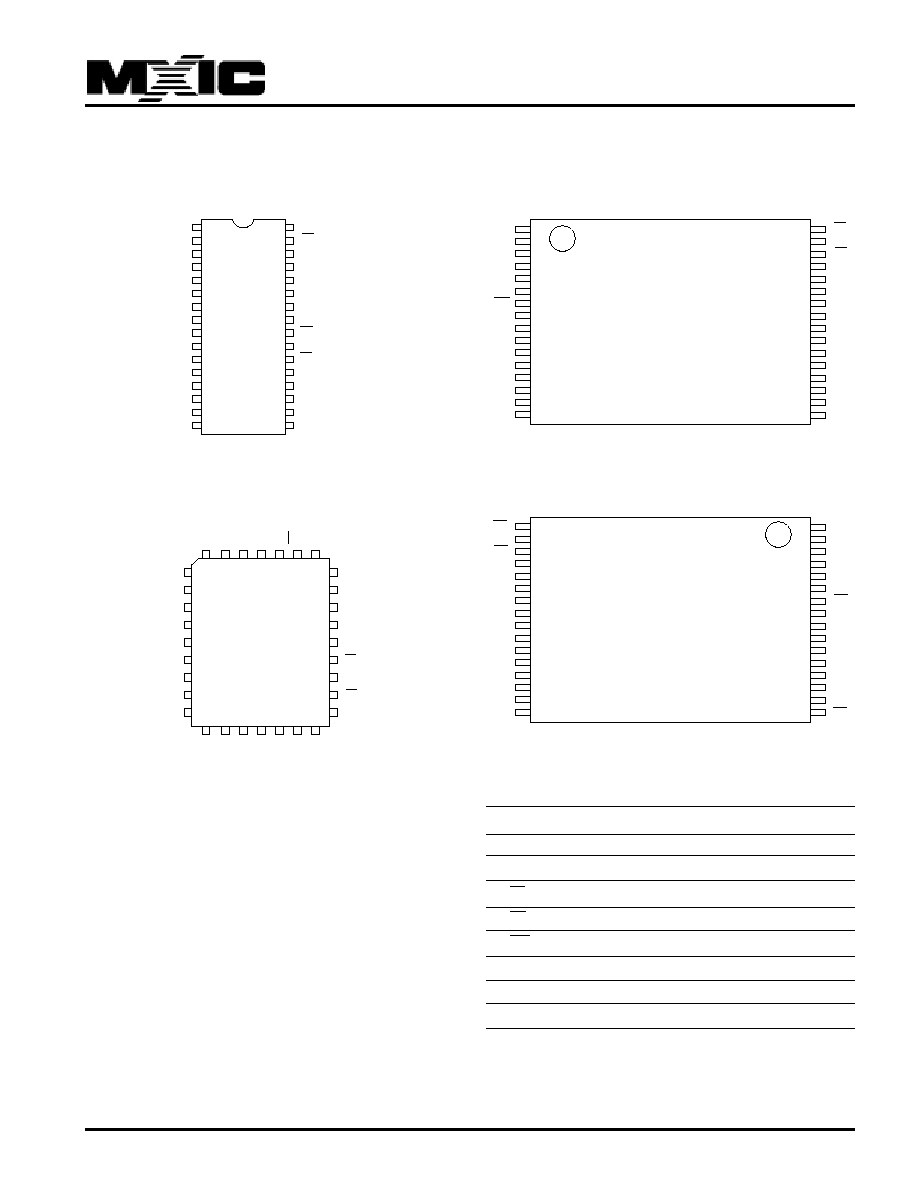
PIN CONFIGURATIONS
32 PDIP
TSOP (TYPE 1)
(REVERSE TYPE)
(NORMAL TYPE)
PIN DESCRIPTION:
32 PLCC
MX28F1000P
1
2
3
4
5
6
7
8
9
10
11
12
13
14
15
16
VPP
A16
A15
A12
A7
A6
A5
A4
A3
A2
A1
A0
Q0
Q1
Q2
GND
32
31
30
29
28
27
26
25
24
23
22
21
20
19
18
17
VCC
WE
NC
A14
A13
A8
A9
A11
OE
A10
CE
Q7
Q6
Q5
Q4
Q3
1
4
5
9
13
14
17
20
21
25
29
32
30
A14
A13
A8
A9
A11
OE
A10
CE
Q7
A7
A6
A5
A4
A3
A2
A1
A0
Q0
Q1
Q2
VSS
Q3
Q4
Q5
Q6
A12
A15
A16
VPP
VCC
WE
NC
MX28F1000P
A11
A9
A8
A13
A14
NC
WE
VCC
VPP
A16
A15
A12
A7
A6
A5
A4
1
2
3
4
5
6
7
8
9
10
11
12
13
14
15
16
OE
A10
CE
Q7
Q6
Q5
Q4
Q3
GND
Q2
Q1
Q0
A0
A1
A2
A3
32
31
30
29
28
27
26
25
24
23
22
21
20
19
18
17
MX28F1000P
OE
A10
CE
Q7
Q6
Q5
Q4
Q3
GND
Q2
Q1
Q0
A0
A1
A2
A3
32
31
30
29
28
27
26
25
24
23
22
21
20
19
18
17
A11
A9
A8
A13
A14
NC
WE
VCC
VPP
A16
A15
A12
A7
A6
A5
A4
1
2
3
4
5
6
7
8
9
10
11
12
13
14
15
16
MX28F1000P
4
P/N: PM0340
REV. 1.6, JAN. 19, 1999
MX28F1000P
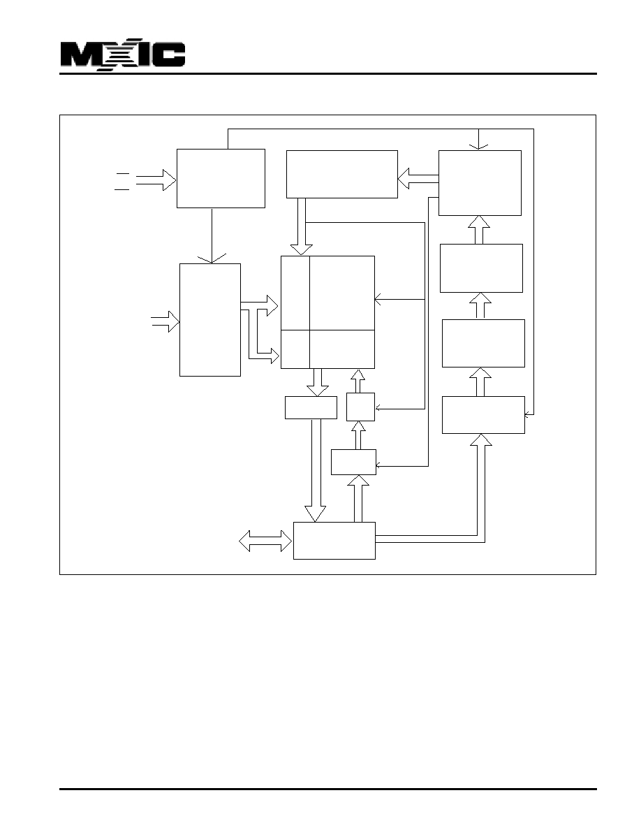
BLOCK DIAGRAM
CONTROL
INPUT
LOGIC
PROGRAM/ERASE
HIGH VOLTAGE
MODE
LOGIC
STATE
REGISTER
MX28F1000P
FLASH
ARRAY
X-DECODER
ADDRESS
LATCH
AND
BUFFER
Y-PASS GATE
Y
-DECODER
ARRAY
SOURCE
HV
COMMAND
DATA
DECODER
COMMAND
DATA LATCH
I/O BUFFER
PGM
DATA
HV
PROGRAM
DATA LATCH
SENSE
AMPLIFIER
Q0-Q7
A0-A16
CE
OE
WE

5
P/N: PM0340
REV. 1.6, JAN. 19, 1999
MX28F1000P
AUTOMATIC PROGRAMMING
The MX28F1000P is byte programmable using the
Automatic Programming algorithm. The Automatic
Programming algorithm does not require the system to
time out or verify the data programmed. The typical
room temperature chip programming time of the
MX28F1000P is less than 5 seconds.
AUTOMATIC CHIP ERASE
The device may be erased using the Automatic Erase
algorithm. The Automatic Erase algorithm automati-
cally programs the entire array prior to electrical erase.
The timing and verification of electrical erase are
controlled internal to the device.
AUTOMATIC BLOCK ERASE
The MX28F1000P is block(s) erasable using MXIC's
Auto Block Erase algorithm. Block erase modes allow
blocks of the array to be erased in one erase cycle.
The Automatic Block Erase algorithm automatically
programs the specified block(s) prior to electrical
erase. The timing and verification of electrical erase
are controlled internal to the device.
AUTOMATIC PROGRAMMING ALGORITHM
MXIC's Automatic Programming algorithm requires
the user to only write a program set-up command and
a program command (program data and address). The
device automatically times the programming pulse
width, provides the program verify, and counts the
number of sequences. A status bit similar to DATA
polling and a status bit toggling between consecutive
read cycles, provide feedback to the user as to the
status of the programming operation.
MXIC's Automatic Erase algorithm requires the user to
only write an erase set-up command and erase com-
mand. The device will automatically pre-program and
verify the entire array. Then the device automatically
times the erase pulse width, provides the erase verify,
and counts the number of sequences. A status bit
similar to DATA polling and a status bit toggling
between consecutive read cycles, provide feedback to
the user as to the status of the erase operation.
Commands are written to the command register using
standard microprocessor write timings. Register con-
tents serve as inputs to an internal state-machine
which controls the erase and programming circuitry.
During write cycles, the command register internally
latches address and data needed for the programming
and erase operations. For system design simplifica-
tion, the MX28F1000P is designed to support either
WE or CE controlled writes. During a system write
cycle, addresses are latched on the falling edge of WE
or CE whichever occurs last. Data is latched on the
rising edge of WE or CE whichever occur first. To
simplify the following discussion, the WE pin is used as
the write cycle control pin throughout the rest of this
text. All setup and hold times are with respect to the
WE signal.
MXIC's Flash technology combines years of EPROM
experience to produce the highest levels of quality, relia-
bility, and cost effectiveness. The MX28F1000P electri-
cally erases all bits simultaneously using Fowler-Nord-
heim tunneling. The bytes are programmed one byte at
a time using the EPROM programming mechanism of hot
electron injection.
AUTOMATIC ERASE ALGORITHM
6
P/N: PM0340
REV. 1.6, JAN. 19, 1999
MX28F1000P
TABLE 1. COMMAND DEFINITIONS
COMMAND
BUS
FIRST BUS CYCLE
SECOND BUS CYCLE
CYCLES
OPERATION
ADDRESS
DATA
OPERATION
ADDRESS
DATA
Read Memory
1
Write
X
00H
Read Identified codes
2
Write
X
90H
Read
IA
ID
Setup auto erase/
2
Write
X
30H
Write
X
30H
auto erase (chip)
Setup auto erase/
2
Write
X
20H
Write
EA
D0H
auto erase (block)
Setup auto program/
2
Write
X
40H
Write
PA
PD
program
Setup Erase/
2
Write
X
20H
Write
X
20H
Erase (chip)
Setup Erase/
2
Write
X
60H
Write
EA
60H
Erase (block)
Erase verify
2
Write
EVA
A0H
Read
X
EVD
Reset
2
Write
X
FFH
Write
X
FFH
Note:
IA
= Identifier address
EA
= Block of memory location to be erased
PA
= Address of memory location to be pro-
grammed
ID
= Data read from location IA during device iden-
tification
PD
= Data to be programmed at location PA
EVA = Address of memory location to be read during
erase verify.
EVD = Data read from location EVA during erase
verify.
Auto modes have the build-in enchanced features.
Please use the auto erase mode whenever it is.

7
P/N: PM0340
REV. 1.6, JAN. 19, 1999
MX28F1000P
COMMAND DEFINITIONS
When low voltage is applied to the VPP pin, the con-
tents of the command register default to 00H, enabling
read-only operation.
Placing high voltage on the VPP pin enables read/write
operations. Device operations are selected by writing
specific data patterns into the command register. Ta-
ble 1 defines these MX28F1000P register commands.
Table 2 defines the bus operations of MX28F1000P.
TABLE 2. MX28F1000P BUS OPERATIONS
OPERATION
VPP(1)
A0
A9
CE
OE
WE
DQ0-DQ7
READ-ONLY
Read
VPPL
A0
A9
VIL
VIL
VIH
Data Out
Output Disable
VPPL
X
X
VIL
VIH
VIH
Tri-State
Standby
VPPL
X
X
VIH
X
X
Tri-State
Read Silicon ID (Mfr)(2)
VPPL
VIL
VID(3)
VIL
VIL
VIH
Data = C2H
Read Silicon ID (Device)(2)
VPPL
VIH
VID(3)
VIL
VIL
VIH
Data = 1AH
READ/WRITE
Read
VPPH
A0
A9
VIL
VIL
VIH
Data Out(4)
Standby(5)
VPPH
X
X
VIH
X
X
Tri-State
Write
VPPH
A0
A9
VIL
VIH
VIL
Data In(6)
NOTES:
1. VPPL may be grounded, a no-connect with a resistor tied
to ground, or < VCC + 2.0V. VPPH is the programming
voltage specified for the device. When VPP = VPPL,
memory contents can be read but not written or erased.
2. Manufacturer and device codes may also be accessed
via a command register write sequence. Refer to Table
1. All other addresses are don't care.
3. VID is the Silicon-ID-Read high voltage.(11.5V to 13v)
4. Read operations with VPP = VPPH may access array
data or Silicon ID codes.
5. With VPP at high voltage, the standby current equals ICC
+ IPP (standby).
6. Refer to Table 1 for valid Data-In during a write operation.
7. X can be VIL or VIH.

8
P/N: PM0340
REV. 1.6, JAN. 19, 1999
MX28F1000P
device returns to the Read mode. The system is not
required to provide any control or timing during these
operations.
When using the Automatic Chip Erase algorithm, note
that the erase automatically terminates when
adequate erase margin has been achieved for the
memory array(no erase verify command is required).
The margin voltages are internally generated in the
same manner as when the standard erase verify
command is used.
The Automatic set-up erase command is a command-
only operation that stages the device for automatic
electrical erasure of all bytes in the array. Automatic
set-up erase is performed by writing 30H to the
command register.
To command automatic chip erase, the command 30H
must be written again to the command register. The
automatic chip erase begins on the rising edge of the
WE and terminates when the data on DQ7 is "1" and
the data on DQ6 stops toggling for two consecutive
read cycles, at which time the device returns to the
Read mode.
SET-UP AUTOMATIC BLOCK ERASE/ERASE
COMMANDS
The automatic block erase does not require the device
to be entirely pre-programmed prior to executing the
Automatic set-up block erase command and
Automatic block erase command. Upon executing the
Automatic block erase command, the device automati-
cally will program and verify the block(s) memory for an
all-zero data pattern. The system is not required to
provide any controls or timing during these operations.
When the block(s) is automatically verified to contain
an all-zero pattern, a self-timed block erase and verify
begin. The erase and verify operations are complete
when the data on DQ7 is "1" and the data on DQ6 stops
toggling for two consecutive read cycles, at which time
the device returns to the Read mode. The system is
not required to provide any control or timing during
these operations.
When using the Automatic Block Erase algorithm, note
that the erase automatically terminates when adequate
erase margin has been achieved for the memory array
(no erase verify command is required). The margin
READ COMMAND
While VPP is high, for erase and programming, mem-
ory contents can also be accessed via the read com-
mand. The read operation is initiated by writing 00H
into the command register. Microprocessor read
cycles retrieve array data. The device remains en-
abled for reads until the command register contents
are altered.
The default contents of the register upon VPP power-
up is 00H. This default value ensures that no spurious
alteration of memory contents occurs during the VPP
power transition. Where the VPP supply is hard-wired
to the MX28F1000P, the device powers up and
remains enabled for reads until the command register
contents are changed.
SILICON-ID-READ COMMAND
Flash-memories are intended for use in applications
where the local CPU alters memory contents. As such,
manufacturer- and device-codes must be accessible
while the device resides in the target system. PROM
programmers typically access signature codes by rais-
ing A9 to a high voltage. However, multiplexing high
voltage onto address lines is not a desired system-
design practice.
The MX28F1000P contains a Silicon-ID-Read
o p e r a t i o n t o s u p p l e m e n t t r a d i t i o n a l P R O M -
programming methodology. The operation is initiated
by writing 90H into the command register. Following
the command write, a read cycle from address 0000H
retrieves the manufacturer code of C2H. A read cycle
from address 0001H returns the device code of 1AH.
SET-UP AUTOMATIC CHIP ERASE/ERASE
COMMANDS
The automatic chip erase does not require the device
to be entirely pre-programmed prior to excuting the
Automatic set-up erase command and Automatic chip
erase command. Upon executing the Automatic chip
erase command, the device automatically will program
and verify the entire memory for an all-zero data
pattern. When the device is automatically verified to
contain an all-zero pattern, a self-timed chip erase and
verify begin. The erase and verify operations are
complete when the data on DQ7 is "1" at which time the

9
P/N: PM0340
REV. 1.6, JAN. 19, 1999
MX28F1000P
SET-UP CHIP ERASE/ERASE COMMANDS
Set-up Chip Erase is a command-only operation that
stages the device for electrical erasure of all bytes in
the array. The set-up erase operation is performed by
writing 20H to the command register.
To commence chip erasure, the erase command (20H)
must again be written to the register. The erase
operation begins with the rising edge of the WE pulse.
This two-step sequence of set-up followed by execu-
tion ensures that memory contents are not accidentally
erased. Also, chip-erasure can only occur when high
voltage is applied to the VPP pin. In the absence of this
high voltage, memory contents are protected against
erasure.
SET-UP BLOCK ERASE/ERASE COMMANDS
Set-up Block Erase is a command-only operation that
stages the device for electrical erasure of all selected
block(s) in the array. The set-up erase operation is
performed by writing 60H to the command register.
To enter block-erasure, the block erase command 60H
must be written again to the command register. The
block erase mode allows 1 to 8 blocks of the array to be
erased in one internal erase cycle. Internally, there are
8 registers (flags) addressed by A14 to A16. First block
address is loaded into internal registers on the 2-nd
falling of WE. Each successive block load cycles,
started by the falling edge of WE, must begin within
30
m
s from the rising edge of the preceding WE. Other-
wise, the loading period ends and internal block erase
cycle starts. When the data on DQ7 is "1" at which time
auto erase ends and the device returns to the Read
mode.
ERASE-VERIFY COMMAND
After each erase operation, all bytes must be verified.
The erase verify operation is initiated by writing A0H
into the command register. The address for the byte to
be verified must be supplied as it is latched on the
falling edge of the WE pulse.
voltages are internally generated in the same manner
as when the standard erase verify command is used.
The Automatic set-up block erase command is a com-
mand only operation that stages the device for auto-
matic electrical erasure of selected blocks in the array.
Automatic set-up block erase is performed by writing
20H to the command register.
To enter automatic block erase, the user must write
the command D0H to the command register. Block
addresses are loaded into internal register on the 2nd
falling edge of WE. Each successive block load cycles,
started by the falling edge of WE, must begin within
30
m
s from the rising edge of the preceding WE.
Otherwise, the loading period ends and internal auto
block erase cycle starts. When the data on DQ7 is "1"
and the data on DQ6 stops toggling for two
consecutive read cycles, at which time auto erase
ends and the device returns to the Read mode.
Refer to page 2 for detailed block address.
SET-UP AUTOMATIC PROGRAM/PROGRAM
COMMANDS
The Automatic Set-up Program is a command-only
operation that stages the device for automatic pro-
gramming. Automatic Set-up Program is performed by
writing 40H to the command register.
Once the Automatic Set-up Program operation is per-
formed, the next WE pulse causes a transition to an
active programming operation. Addresses are
internally latched on the falling edge of the WE pulse.
Data is internally latched on the rising edge of the WE
pulse. The rising edge of WE also begins the
programming operation. The system is not required to
provide further controls or timings. The device will
automatically provide an adequate internally
generated program pulse and verify margin. The
automatic programming operation is completed when
the data read on DQ6 stops toggling for two
consecutive read cycles and the data on DQ7 and
DQ6 are equivalent to data written to these two bits, at
which time the device returns to the Read mode (no
program verify command is required).

10
P/N: PM0340
REV. 1.6, JAN. 19, 1999
MX28F1000P
DATA POLLING-DQ7
The MX28F1000P also features Data Polling as a
method to indicate to the host system that the
Automatic Program or Erase algorithms are either in
progress or completed.
While the Automatic Programming algorithm is in op-
eration, an attempt to read the device will produce the
complement data of the data last written to DQ7. Upon
completion of the Automatic Program algorithm an
attempt to read the device will produce the true data
last written to DQ7. The Data Polling feature is valid
after the rising edge of the second WE pulse of the two
write pulse sequences.
While the Automatic Erase algorithm is in operation,
DQ7 will read "0" until the erase operation is com-
pleted. Upon completion of the erase operation, the
data on DQ7 will read "1". The Data Polling feature is
valid after the rising edge of the second WE pulse of
two write pulse sequences.
The Data Polling feature is active during Automatic
Program/Erase algorithms.
POWER-UP SEQUENCE
The MX28F1000P powers up in the Read only mode. In
addition, the memory contents may only be altered after
successful completion of a two-step command sequence.
Power up sequence is not required.
SYSTEM CONSIDERATIONS
During the switch between active and standby condi-
tions, transient current peaks are produced on the
rising and falling edges of Chip Enable. The magnitude
of these transient current peaks is dependent on the
output capacitance loading of the device. At a
minimum, a 0.1uF ceramic capacitor (high frequency,
low inherent inductance) should be used on each
device between VCC and GND, and between VPP and
GND to minimize transient effects. In addition, to
overcome the voltage drop caused by the inductive
effects of the printed circuit board traces on FLASH
memory arrays, a 4.7uF bulk electrolytic capacitor
should be used between VCC and GND for each eight
devices. The location of the capacitor should be close
to where the power supply is connected to the array.
The MX28F1000P applies an internally generated
margin voltage to the addressed byte. Reading FFH
from the addressed byte indicates that all bits in the
byte are erased.
The erase-verify command must be written to the
command register prior to each byte verification to
latch its address. The process continues for each byte
in the array until a byte does not return FFH data, or the
last address is accessed.
In the case where the data read is not FFH, another
erase operation is performed. (Refer to Set-up Erase/
Erase). Verification then resumes from the address of
the last-verified byte. Once all bytes in the array have
been verified, the erase step is complete. The device
can be programmed. At this point, the verify operation
is terminated by writing a valid command (e.g.
Program Set-up) to the command register. The High
Reliability Erase algorithm, illustrates how commands
and bus operations are combined to perform electrical
erasure of the MX28F1000P.
RESET COMMAND
A reset command is provided as a means to safely
abort the erase- or program-command sequences.
Following either set-up command (erase or program)
with two consecutive writes of FFH will safely abort the
operation. Memory contents will not be altered.
Should program-fail or erase-fail happen, two
consecutive writes of FFH will reset the device to abort
the operation. A valid command must then be written
to place the device in the desired state.
WRITE OPERATON STATUS
TOGGLE BIT-DQ6
The MX28F1000P features a "Toggle Bit" as a method
to indicate to the host sytem that the Auto Program/
Erase algorithms are either in progress or completed.
While the Automatic Program or Erase algorithm is in
progress, successive attempts to read data from the
device will result in DQ6 toggling between one and
zero. Once the Automatic Program or Erase algorithm
is completed, DQ6 will stop toggling and valid data will
be read. The toggle bit is valid after the rising edge of
the second WE pulse of the two write pulse
sequences.
11
P/N: PM0340
REV. 1.6, JAN. 19, 1999
MX28F1000P
ABSOLUTE MAXIMUM RATINGS
RATING
VALUE
Ambient Operating Temperature
-40
o
C to 85
o
C
Storage Temperature
-65
o
C to 125
o
C
Applied Input Voltage
-0.5V to 7.0V
Applied Output Voltage
-0.5V to 7.0V
VCC to Ground Potential
-0.5V to 7.0V
A9 & VPP
-0.5V to 13.5V
NOTICE:
Stresses greater than those listed under ABSOLUTE MAXI-
MUM RATINGS may cause permanent damage to the de-
vice. This is stress rating only and functional operational
sections of this specification is not implied. Exposure to ab-
solute maximum rating conditions for extended period may
affect reliability.
NOTICE:
Specifications contained within the following tables are sub-
ject to change.
CAPACITANCE TA = 25
o
C, f = 1.0 MHz
SYMBOL
PARAMETER
MIN.
TYP
MAX.
UNIT
CONDITIONS
CIN
Input Capacitance
14
pF
VIN = 0V
COUT
Output Capacitance
16
pF
VOUT = 0V
READ OPERATION
DC CHARACTERISTICS
SYMBOL
PARAMETER
MIN.
TYP
MAX.
UNIT
CONDITIONS
ILI
Input Leakage Current
10
uA
VIN = GND to VCC
ILO
Output Leakage Current
10
uA
VOUT = GND to VCC
IPP1
VPP Current
1
100
uA
VPP = 5.5V
ISB1
Standby VCC current
1
mA
CE = VIH
ISB2
1
100
uA
CE = VCC + 0.3V
ICC1
Operating VCC current
30(NOTE4) mA
IOUT = 0mA, f=1MHz
ICC2
50
mA
IOUT = 0mA, f=11MHz
VIL
Input Low Voltage
-0.3
(NOTE 1)
0.8
V
VIH
Input High Voltage
2.4
VCC + 0.3
V
VOL
Output Low Voltage
0.45
V
IOL = 2.1mA
VOH
Output High Voltage
2.4
V
IOH = -400uA
NOTES:
1. VIL min. = -1.0V for pulse width < 50 ns.
VIL min. = -2.0V for pulse width < 20 ns.
2. VIH max. = VCC + 1.5V for pulse width < 20 ns
If VIH is over the specified maximum value, read operation
cannot be guaranteed.
3. Test condition:
TA =-40
∞
C to 85
∞
C, Vcc = 5V
±
10%, Vpp = GND to Vcc, CL
= 100pF(for MX28F1000P-90/12)
TA = -40
∞
C to 85
∞
C, Vcc = 5V
±
10%, Vpp = GND to Vcc, CL
= 35pF(for MX28F1000P-70)
4.ICC1=35mA for TA=-40
∞
C to 85
∞
C
12
P/N: PM0340
REV. 1.6, JAN. 19, 1999
MX28F1000P
NOTE:
1. tDF is defined as the time at which the output achieves the
open circuit condition and data is no longer driven.
TEST CONDITIONS:
∑ Input pulse levels: 0.45V/2.4V
∑ Input rise and fall times:
<
10ns
∑ Reference levels for measuring timing: 0.8V, 2.0V
∑ 28F1000P-70:Vcc = 5V
±
5%, CL: 1TTL gate +
35pF(including scope and jig)
∑ 28F1000P-70:Vcc = 5V
±
5%, CL: 1TTL gate +
35pF(including scope and jig)
∑ Vpp = GND to Vcc
AC CHARACTERISTICS
28F1000P-70
28F1000P-90
28F1000P-12
SYMBOL
PARAMETER
MIN.
MAX.
MIN.
MAX.
MIN.
MAX.
UNIT
CONDITIONS
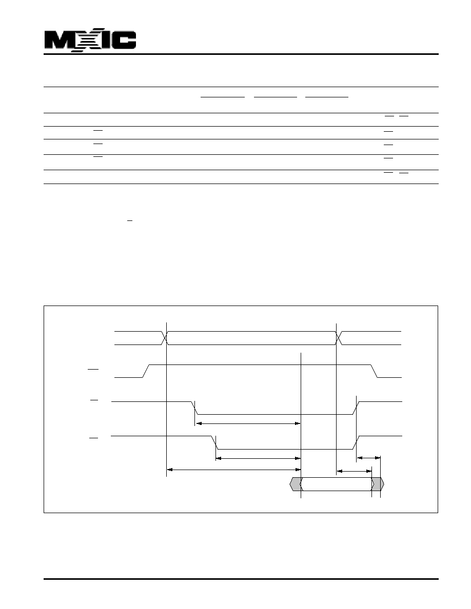
tACC
Address to Output Delay
70
90
120
ns
CE=OE=VIL
tCE
CE to Output Delay
70
90
120
ns
OE=VIL
tOE
OE to Output Delay
30
35
50
ns
CE=VIL
tDF
OE High to Output Float
(
Note1)
0
15
0
20
0
30
ns
CE=VIL
tOH
Address to Output hold
0
0
0
0
ns
CE=OE=VIL
READ TIMING WAVEFORMS
ADDRESS
WE
OE
CE
tOH
tDF
tACC
tOE
tCE
ACTIVE MODE
STANDBY MODE
STANDBY MODE
DATA OUT
DATA OUT VALID

13
P/N: PM0340
REV. 1.6, JAN. 19, 1999
MX28F1000P
COMMAND PROGRAMMING/DATA PROGRAMMING/ERASE OPERATION
DC CHARACTERISTICS
SYMBOL
PARAMETER
MIN.
TYP
MAX.
UNIT
CONDITIONS
ILI
Input Leakage Current
10
uA
VIN=GND to VCC
ILO
Output Leakage Current
10
uA
VOUT=GND to VCC
ISB1
Standby VCC current
1
mA
CE=VIH
ISB2
1
100
uA
CE=VCC
±
0.3V
ICC1 (Read)
Operating VCC Current
30
mA
IOUT=0mA, f=1MHz
ICC2
50
mA
IOUT=0mA, F=11MHz
ICC3 (Program)
50
mA
In Programming
ICC4 (Erase)
50
mA
In Erase
ICC5 (Program Verify)
50
mA
In Program Verify
ICC6 (Erase Verify)
50
mA
In Erase Verify
IPP1 (Read)
VPP Current
100
uA
VPP=12.6V
IPP2 (Program)
50
mA
In Programming
IPP3 (Erase)
50
mA
In Erase
IPP4 (Program Verify)
50
mA
In Program Verify
IPP5 (Erase Verify)
50
mA
In Erase Verify
VIL
Input Voltage
-0.3 (Note 5)
0.8
V
VIH
2.4
VCC+0.3V V
(Note 6)
VOL
Output Voltage
0.45
V
IOL=2.1mA
VOH
2.4
V
IOH=-400uA
NOTES:
1. VCC must be applied before VPP and removed after VPP.
2. VPP must not exceed 14V including overshoot.
3. An influence may be had upon device reliability if the device
is installed or removed while VPP=12V.
4. Do not alter VPP either VIL to 12V or 12V to VIL when
CE=VIL.
5. VIL min. = -0.6V for pulse width
<
20ns.
6. If VIH is over the specified maximum value, programming
operation cannot be guranteed.
7. All currents are in RMS unless otherwise noted.(Sampled, not
100% tested.)
8. For 28F1000P-70, Vcc = 5V
±
5%, CL = 35pF; for 28F1000P-
90/12, Vcc = 5V
±
10%, CL = 100pF.
14
P/N: PM0340
REV. 1.6, JAN. 19, 1999
MX28F1000P
AC CHARACTERISTICS
TA = -40
o
C to 85
o
C, VCC = 5V
±
10%, VPP =12V
±
5%
28F1000-70
28F1000P-90
28F1000P-12
SYMBOL PARAMETER
MIN.
MAX.
MIN.
MAX.
MIN.
MAX.
UNIT
CONTIONS
tVPS
VPP setup time
100
100
100
ns
tOES
OE setup time
100
100
100
ns
tCWC
Command programming cycle
70
90
120
ns
tCEP
WE programming pulse width
40
45
50
ns
tCEPH1
WE programming pluse width High
20
20
20
ns
tCEPH2
WE programming pluse width High
100
100
100
ns
tAS
Address setup time
0
0
0
ns
tAH
Address hold time
40
45
50
ns
tAH1
Address hold time for DATA POLLING
0
0
0
ns
tDS
Data setup time
40
45
50
ns
tDH
Data hold time
10
10
10
ns
tCESP
CE setup time before DATA polling/toggle bit 100
100
100
ns
tCES
CE setup time
0
0
0
ns
tCESC
CE setup time before command write
100
100
100
ns
tCESV
CE setup time before verify
6
6
6
us
tVPH
VPP hold time
100
100
100
ns
tDF
Output disable time (Note 3)
15
20
30
ns
tDPA
DATA polling/toggle bit access time
70
90
120
ns
tAETC
Total erase time in auto chip erase
5(TYP.)
5(TYP.)
5(TYP.)
s
tAETB
Total erase time in auto block erase
5TYP.)
5(TYP.)
5(TYP.)
s
tAVT
Total programming time in auto verify
15
300
15
300
15
300
us
tBALC
Block address load cycle
0.3
30
0.3
30
0.3
30
us
tBAL
Block address load time
200
200
200
us
tCH
CE Hold Time
0
0
0
ns
tCS
CE setup to WE going low
0
0
0
ns
NOTES:
1. CE and OE must be fixed high during VPP transition from 5V
to 12V or from 12V to 5V.
2. Refer to read operation when VPP=VCC about read opera-
tion while VPP 12V.
3. tDF defined as the time at which the output achieves the open
circuit condition and data is no longer driven.
15
P/N: PM0340
REV. 1.6, JAN. 19, 1999
MX28F1000P
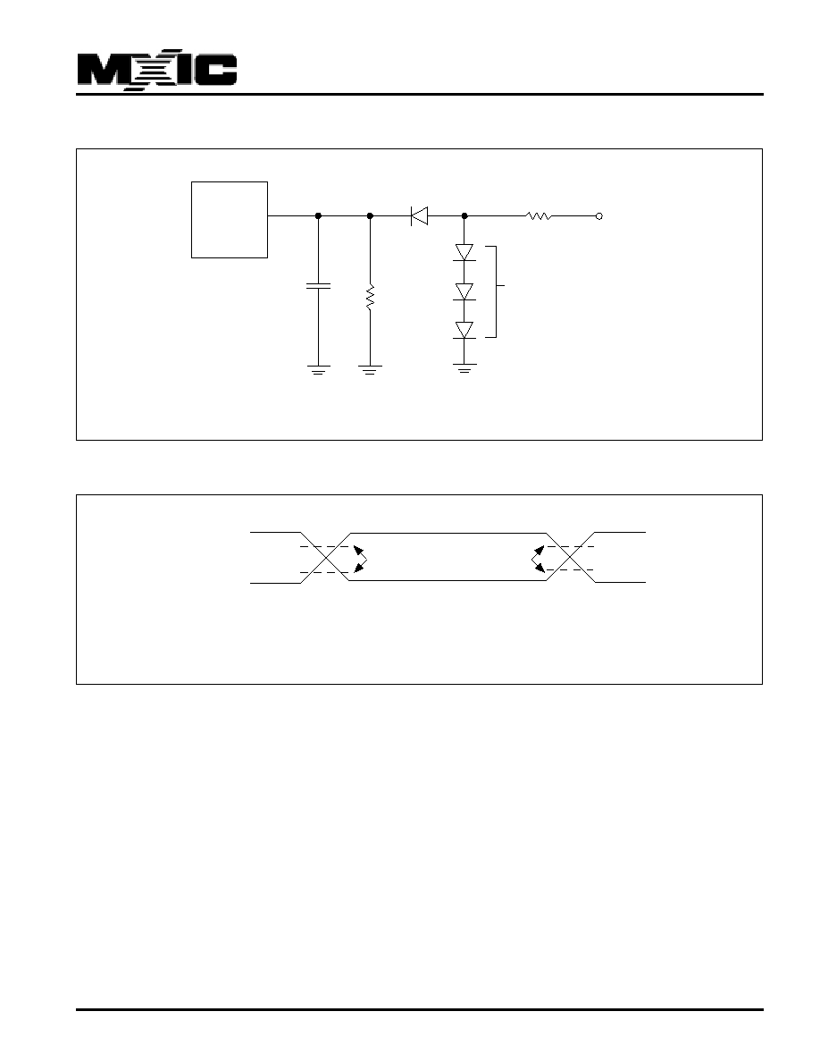
SWITCHING TEST CIRCUITS
SWITCHING TEST WAVEFORMS
2.0V
2.4 V
0.45 V
0.8V
TEST POINTS
INPUT
2.0V
0.8V
OUTPUT
AC TESTING: Inputs are driven at 2.4V for a logic "1" and 0.45V for a logic "0".
Input pulse rise and fall times are <20ns.
DEVICE
UNDER
TEST
DIODES = IN3064
OR EQUIVALENT
CL = 100 pF including jig capacitance(35pF for 70 ns parts)
6.2K ohm
1.8K ohm
+5V
CL

16
P/N: PM0340
REV. 1.6, JAN. 19, 1999
MX28F1000P
AUTOMATIC PROGRAMMING TIMING WAVEFORM
One byte data is programmed. Verify in fast algorithm
and additional programming by external control are not
required because these operations are excuted auto-
matically by internal control circuit. Programming
completion can be verified by DATA polling and toggle bit
checking after automatic verify starts. Device outputs
DATA during programming and DATA after programming
on Q7. Q0 to Q5 (Q6 is for toggle bit; see toggle bit, DATA
polling, timing waveform) are in high impedance.
tCWC
Address
valid
tAS
tCEP
tOES
tCEP
tCESP tCES
tCESC
tDS
tDH
tDH
tDS
tDF
Data in
Command in
Data in
Command in
Vcc 5V
CE
OE
tAVT
12V
Vpp
0V
Command #40H
tVPH
tVPS
Q7
Q0~Q5
DATA polling
Auto program & DATA polling
Setup auto program/
program command
DATA
DATA
WE
A0 ~ A16
tCEPH1
tAH1
DATA
tDPA
17
P/N: PM0340
REV. 1.6, JAN. 19, 1999
MX28F1000P
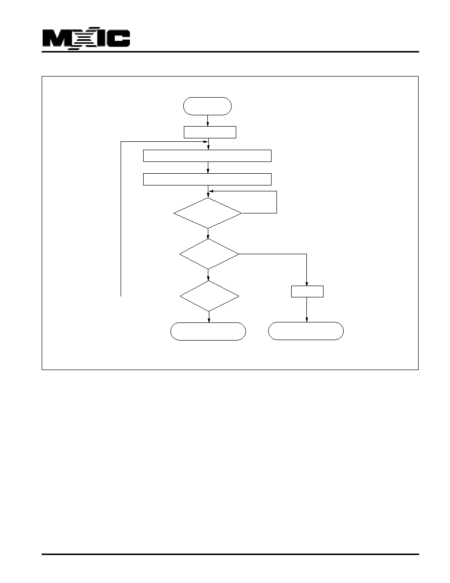
AUTOMATIC PROGRAMMING ALGORITHM FLOWCHART
START
Apply VppH
Write Set up auto program Command (40H)
NO
Toggle Bit Checking
DQ6 not Toggled
Write Auto program Command(A/D)
Last Byte
Auto Program Completed
YES
YES
NO
Verify Byte Ok
Auto Program Failed
NO
YES
Reset
18
P/N: PM0340
REV. 1.6, JAN. 19, 1999
MX28F1000P
erase starts. Device outputs 0 during erasure and 1 after
erasure on Q7. Q0 to Q5 (Q6 is for toggle bit; see toggle
bit, DATA polling, timing waveform) are in high imped-
ance.
AUTOMATIC CHIP ERASE TIMING WAVEFORM
All data in chip are erased. External erase verify is not
required because data is erased automatically by internal
control circuit. Erasure completion can be verified by
DATA polling and toggle bit checking after automatic
tCWC
tCEP
tOES
tCEP
tCESP tCES
tCESC
tDS
tDH
tDH
tDS
tDF
Command in
Command in
Vcc 5V
CE
OE
tAETC
Command in
Command in
12V
Vpp
0V
Command #30H Command #30H
tVPH
tVPS
Q7
Q0~Q5
Auto chip erase & DATA polling
DATA polling
A0 ~ A16
WE
tCEPH1
Setup auto chip erase/
erase command
tDPA
19
P/N: PM0340
REV. 1.6, JAN. 19, 1999
MX28F1000P
AUTOMATIC CHIP ERASE ALGORITHM FLOWCHART
START
Apply VppH
Write Set up auto chip Erase Command (30H)
Toggle Bit Checking
DQ6 not Toggled
Write Auto chip Erase Command(30H)
DATA Polling
DQ7 = 1
Auto Chip Erase Completed
YES
YES
Auto Chip Erase Failed
Reset
No
No

20
P/N: PM0340
REV. 1.6, JAN. 19, 1999
MX28F1000P
checking after automatic erase starts. Device outputs 0
during erasure and 1 after erasure on Q7. Q0 to Q5 (Q6
is for toggle bit; see toggle bit, DATA polling, timing
waveform) are in high impedance.
AUTOMATIC BLOCK ERASE TIMING WAVEFORM
Block data indicated by A12 to A16 are erased. External
erase verify is not required because data are erased
automatically by internal control circuit. Erasure comple-
tion can be verified by DATA polling and toggle bit
*Refer to page 2 for detailed block address.
Vcc 5V
tCEP
tOES
tDF
Command in
OE
Command in
Command in
Command in
tCESC
tDS
tDH
tDS
tDH
Block
address 0
Block
address 1
tCWC
tAS
tAH
tBALC
tCEP
12V
Vpp
0V
Block
address #
Command #20H Command #D0H
tVPH
tVPS
tBAL
tAETB
Q7
Q0~Q5
Auto block erase & DATA polling
DATA polling
A12 ~ A16
CE
WE
tCEPH2
tCEPH1
tCH
tCS
tAH1
Setup auto block erase/erase command
tDPA
A0 ~ A11

21
P/N: PM0340
REV. 1.6, JAN. 19, 1999
MX28F1000P
AUTOMATIC BLOCK ERASE ALGORITHM FLOWCHART
START
Apply VppH
Write Set up auto block Erase Command (20H)
NO
Write Auto block Erase Command(D0H)
to Load Block Address
Toggle Bit Checking
DQ6 not Toggled
Auto Block Erase Completed
YES
Last Block
to Erase
Wait 200us
YES
DATA Polling
DQ7 = 1
Reset
Auto Block Erase Failed
NO
NO
YES
Load Block Address

22
P/N: PM0340
REV. 1.6, JAN. 19, 1999
MX28F1000P
COMPATIBLE CHIP ERASE TIMING WAVEFORM
All data in chip are erased. Control verification and
additional erasure externally according tocompatible chip
erase flowchart.
Vcc 5V
tCEP
tOES
tDF
Command in
CE
OE
Command in
tCESC
tCEP
tDS
tDH
tDS
tDH
tCWC
tET
tCEP
tCES
tVA
Command in
Command in
tDS
12V
Vpp
0V
Command #20H Command #20H
Command #A0H
tVPH
tVPS
Q7
Q0~Q6
Erase Verify
Chip erase
tAS tAH
Verify
Address
tCESV
Command in
Command in
tDH
Data valid
Data valid
A0 ~ A16
WE
tCEPH1
Setup chip erase/
erase command
23
P/N: PM0340
REV. 1.6, JAN. 19, 1999
MX28F1000P
COMPATIBLE BLOCK ERASE
This device can be applied to the compatible block erase
algorithm shown in the following flowchart. This algorithm
allows to obtain faster erase time by the block (16K byte
x 8 block) without any voltage stress to the device nor
deterioration in reliability of data.
BLOCK ERASE FLOW
COMPATIBLE BLOCK ERASE FLOWCHART
START
Apply
WRITE SETUP BLOCK ERASE COMMAND
END
VPP = VPPH
WRITE BLOCK ERASE COMMAND
( 60H )
WAIT
10 ms
( LOAD FIRST SECTOR ADDRESS , 60H )
LOAD OTHER SECTORS' ADDRESS
IF NECESSARY
( LOAD OTHER SECTOR ADDRESS )
START
END
NO
YES
FAIL
ALL BITS VERIFIED
N = 0
BLOCK ERASE FLOW
ERSVFY FLOW
N = 1024?
BLOCK ERASE FAIL
APPLY
VPP = VCC
BLOCK ERASE
COMPLETE
N = N+1
For selected block(s),
All bits PGM"0"

24
P/N: PM0340
REV. 1.6, JAN. 19, 1999
MX28F1000P
ERASE VERIFY FLOW
START
WRITE ERASE VERIFY COMMAND
WAIT 6 us
LAST ADDRESS ?
INCREMENT ADDRESS
NO
YES
NO
YES
APPLY
VPP = VPPH
ADDRESS =
FIRST ADDRESS OF ERASED BLOCKS
OR LAST VERIFY FAILED ADDRESS
( A0H )
ERSVFY
FFH ?
ERASE VERIFY
COMPLETE
GO TO ERASE FLOW
AGAIN OR ABORT
25
P/N: PM0340
REV. 1.6, JAN. 19, 1999
MX28F1000P
COMPATIBLE BLOCK ERASE TIMING WAVEFORM
Indicated block data (16 Kbyte) are erased. Control
verification and additional erasure externally according to
compatible block erase flowchart.
Vcc 5V
tDS
tDF
Command in
Command in
tDS
tDH
tDS
tDH
tVA
Command in
Command in
Command in
Command in
tDH
tBAL
tET
tCEP
tAS tAH
tCESC
tOES tCEP
tCEP
tCWC
tBALC
Block
address 0
Block
address 1
tAS tAH
A0 ~ A13
CE
OE
12V
Vpp
0V
Command #60H Command #60H
Command #A0H
tVPH
tVPS
Q7
Q0~Q6
Erase Verify
Block erase
tCESV
tCES
Data valid
Data valid
Verify
address
Verify
address
A14 ~ A16
WE
Block
address #
tCEPH1
tCEPH2
Setup block erase/erase command
26
P/N: PM0340
REV. 1.6, JAN. 19, 1999
MX28F1000P
VPP LOW ID CODE READ TIMING WAVEFORM
VPP HIGH READ TIMING WAVEFORM
tACC
tCE
tACC
tOE
tOH
tOH
tDF
Manufacturer code
Device code
C2H
1AH
VID
VIH
VIL
A9
A0
A1 - A8
A10-A16
CE
OE
Q0 - Q7
WE
VIH
tVPS
Address valid
tACC
tVPH
tCESC
tCWC
tOES
tCEP
tCE
tOES
tDF
tOH
tDS
tDH
tOE
Command in
Data out valid
Vcc 5V
12V
Vpp
0V
A0 - A16
CE
OE
Q0-Q7
00H
tCEPH1
WE

27
P/N: PM0340
REV. 1.6, JAN. 19, 1999
MX28F1000P
VPP HIGH ID CODE READ TIMING WAVEFORM
RESET TIMING WAVEFORM
tCWC
tVPS
Address Valid 0 or 1
tACC
tVPH
tCESC
tOES
tCEP
tCE
tOES
tDF
tOH
tDS
tDH
tOE
Command in
Data out valid
Vcc 5V
12V
Vpp
0V
A0
CE
OE
Q0-Q7
90H
C2H or 1AH
A1 - A16
tCEPH2
WE
tVPS
tCWC
tOES
tCEP
Command in
Vcc 5V
12V
Vpp
0V
CE
OE
Q0-Q7
FFH
FFH
A0 - A16
tCEP
tDS
tDH
tDS
tDH
Command in
tCEPH1
WE
28
P/N: PM0340
REV. 1.6, JAN. 19, 1999
MX28F1000P
Toggle bit appears in Q6, when program/erase is
opperating. DATA polling appears in Q7 during pro-
gramming or erase.
TOGGLE BIT, DATA POLLING TIMING WAVEFORM
HIGH-Z
HIGH-Z
HIGH-Z
HIGH-Z
DATA
DATA
DATA
DATA
DATA
DATA
Vpp 12V
CE
OE
Q6
DURING P/E
Q7
DURING P
Q7
DURING E
Q0~Q5
DATA POLLING
DATA POLLING
PROGRAM/ERASE COMPLETE
TOGGLE BIT
HIGH
WE
LIMITS
PARAMETER
MIN.
TYP.
MAX.
UNITS
Chip/Sector Erase Time
1.5
20
sec
Chip Programming Time
2
13.8
sec
Erase/Program Cycles
10,000
cycles
Byte Program Time
15
642
us
ERASE AND PROGRAMMING PERFORMANCE

29
P/N: PM0340
REV. 1.6, JAN. 19, 1999
MX28F1000P
ORDERING INFORMATION
PLASTIC PACKAGE
PART NO.
ACCESS TIME
OPERATING
STANDBY
PACKAGE
ERASE/PROGRAM
CURRENT
CURRENT
CYCLE
(ns)
MAX.(mA)
MAX.(uA)
MIN.(time)
MX28F1000PPC-70C4
70
50
100
32 Pin DIP
10,000
MX28F1000PPC-90C4
90
50
100
32 Pin DIP
10,000
MX28F1000PPC-12C4
120
50
100
32 Pin DIP
10,000
MX28F1000PQC-70C4
70
50
100
32 Pin PLCC
10,000
MX28F1000PQC-90C4
90
50
100
32 Pin PLCC
10,000
MX28F1000PQC-12C4
120
50
100
32 Pin PLCC
10,000
MX28F1000PTC-70C4
70
50
100
32 Pin TSOP
10,000
(Normal Type)
MX28F1000PTC-90C4
90
50
100
32 Pin TSOP
10,000
(Normal Type)
MX28F1000PTC-12C4
120
50
100
32 Pin TSOP
10,000
(Normal Type)
MX28F1000PRC-70C4
70
50
100
32 Pin TSOP
10,000
(Reverse Type)
MX28F1000PRC-90C4
90
50
100
32 Pin TSOP
10,000
(Reverse Type)
MX28F1000PRC-12C4
120
50
100
32 Pin TSOP
10,000
(Reverse Type)
MX28F1000PPI-70
70
50
100
32 Pin DIP
10,000
MX28F1000PPI-90
90
50
100
32 Pin DIP
10,000
MX28F1000PPI-12
120
50
100
32 Pin DIP
10,000
MX28F1000PQI-70
70
50
100
32 Pin PLCC
10,000
MX28F1000PQI-90
90
50
100
32 Pin PLCC
10,000
MX28F1000PQI-12
120
50
100
32 Pin PLCC
10,000
MX28F1000PTI-70
70
50
100
32 Pin TSOP
10,000
(Normal Type)
MX28F1000PTI-90
90
50
100
32 Pin TSOP
10,000
(Normal Type)
MX28F1000PTI-12
120
50
100
32 Pin TSOP
10,000
(Normal Type)
MX28F1000PRI-70
70
50
100
32 Pin TSOP
10,000
(Reverse Type)
MX28F1000PRI-90
90
50
100
32 Pin TSOP
10,000
(Reverse Type)
MX28F1000PRI-12
120
50
100
32 Pin TSOP
10,000
(Reverse Type)

30
P/N: PM0340
REV. 1.6, JAN. 19, 1999
MX28F1000P
PACKAGE INFORMATION
32-PIN PLASTIC DIP
ITEM
MILLIMETERS
INCHES
A
42.13 max.
1.660 max.
B
1.90 [REF]
.075 [REF]
C
2.54 [TP]
.100 [TP]
D
.46 [Typ.]
.050 [Typ.]
E
38.07
1.500
F
1.27 [Typ.]
.050 [Typ.]
G
3.30
±
.25
.130
±
.010
H
.51 [REF]
.020 [REF]
I
3.94
±
.25
1.55
±
.010
J
5.33 max.
.210 max.
K
15.22
±
.25
.600
±
.101
L
13.97
±
.25
.550
±
.010
M
.25 [Typ.]
.010 [Typ.]
NOTE: Each lead certerline is located within
.25mm[.01 inch] of its true position [TP] at a
maximum at maximum material condition.
32-PIN PLASTIC LEADED CHIP CARRIER (PLCC)
ITEM
MILLIMETERS
INCHES
A
12.44
±
.13
.490
±
.005
B
11.50
±
.13
.453
±
.005
C
14.04
±
.13
.553
±
.005
D
14.98
±
.13
.590
±
.005
E
1.93
.076
F
3.30
±
.25
.130
±
.010
G
2.03
±
.13
.080
±
.005
H
.51
±
.13
.020
±
.005
I
1.27 [Typ.]
.050 [Typ.]
J
.71 [REF]
.028 [REF]
K
.46 [REF]
.018 [REF]
L
10.40/12.94
.410/.510
(W) (L)
(W) (L)
M
.89R
.035R
N
.25[Typ.]
.010[Typ.]
NOTE: Each lead certerline is located within
.25mm[.01 inch] of its true position [TP] at a
maximum at maximum material condition.
1
B
A
4
5
9
13
14
17
20
21
25
29
32
C
D
E
F
G
H
I
K
J
L
M
N
30
A
17
32
16
1
F
D
E
C
B
H
I
J
G
M
0~15°
K
L
31
P/N: PM0340
REV. 1.6, JAN. 19, 1999
MX28F1000P
32-PIN PLASTIC TSOP
ITEM
MILLIMETERS
INCHES
A
20.0
±
.20
.078
±
.006
B
18.40
±
.10
.724
±
.004
C
8.20 max.
.323 max.
D
0.15 [Typ.]
.006 [Typ.]
E
.80 [Typ.]
.031 [Typ.]
F
.20
±
.10
.008
±
.004
G
.30
±
.10
.012
±
.004
H
.50 [Typ.]
.020 [Typ.]
I
.45 max.
.018 max.
J
0 ~ .20
0 ~ .008
K
1.00
±
.10
.039
±
.004
L
1.27 max.
.050 max.
M
.50
.020
N
0 ~5∞
.500
NOTE: Each lead certerline is located within
.25mm[.01 inch] of its true position [TP] at a
maximum at maximum material condition.
A
B
C
D
E
F
G
H
I
J
K
L
M
N
O

32
P/N: PM0340
REV. 1.6, JAN. 19, 1999
MX28F1000P
Note. Revision History
Revision #
Description
Page
Date
1.4
Fast access time 150ns and 1,000 times erase cycles removed.
Tsop pin configuration diagram rotated 180
∞
.
The flow chart of block erase corrected.
1.5
Fast access time 70ns added.
Dec/26/1996
1.6
1)Absolute max. ratings:TA=-40
∞
C to 85
∞
C
P11
JAN/19/1999
2)DC Characteristics:ICC1=35mA for TA=-40
∞
C to 85
∞
C
3)AC Characteristics:TA=-40
∞
C to 85
∞
C
P14
4)Order Informance:Add Industrial Grade
P29
5)Erase & Programming Performance:New in Creased table

33
MX28F1000P
M
ACRONIX
I
NTERNATIONAL
C
O.,
L
TD.
HEADQUARTERS:
TEL:+886-3-578-8888
FAX:+886-3-578-8887
EUROPE OFFICE:
TEL:+32-2-456-8020
FAX:+32-2-456-8021
JAPAN OFFICE:
TEL:+81-44-246-9100
FAX:+81-44-246-9105
SINGAPORE OFFICE:
TEL:+65-747-2309
FAX:+65-748-4090
TAIPEI OFFICE:
TEL:+886-3-509-3300
FAX:+886-3-509-2200
M
ACRONIX
A
MERICA,
I
NC.
TEL:+1-408-453-8088
FAX:+1-408-453-8488
CHICAGO OFFICE:
TEL:+1-847-963-1900
FAX:+1-847-963-1909
http : //www.macronix.com
MACRONIX INTERNATIONAL CO., LTD. reserves the rignt to change product and specifications without notice.