FEATURES
∑ 262,144 bytes by 8-bit organization
∑ Fast access time: 90/120 ns
∑ Low power consumption
≠ 50mA maximum active current
≠ 100uA maximum standby current
∑ Programming and erasing voltage 12V
±
5%
∑ Command register architecture
≠ Byte Programming (15us typical)
≠ Auto chip erase 5 seconds typical
(including preprogramming time)
≠ Block Erase
∑ Optimized high density blocked architecture
≠ Eight 4-KB blocks
≠ Fourteen 16-KB blocks
1
P/N: PM0472
∑ Auto Erase (chip & block) and Auto Program
≠ DATA polling
≠ Toggle bit
∑ 10,000 minimum erase/program cycles
∑ Latch-up protected to 100mA from -1 to VCC+1V
∑ Advanced CMOS Flash memory technology
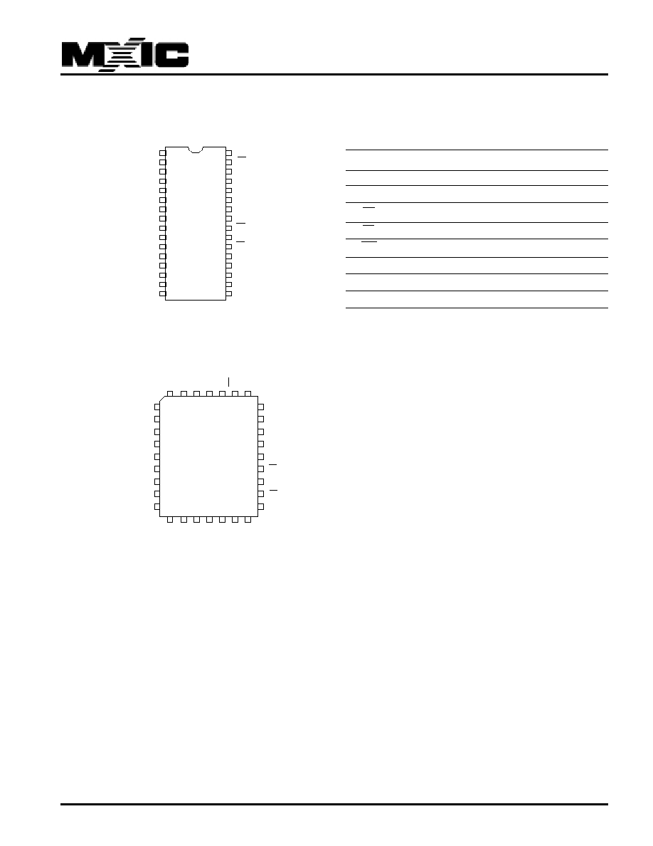
∑ Compatible with JEDEC-standard byte-wide 32-pin
EPROM pinouts
∑ Package type:
≠ 32-pin plastic DIP
≠ 32-pin PLCC
REV. 1.0, Jun 13, 1997
GENERAL DESCRIPTION
The MX28F2000T is a 2-mega bit Flash memory or-
ganized as 256K bytes of 8 bits each. MXIC's Flash
memories offer the most cost-effective and reliable
read/write non-volatile random access memory. The
MX28F2000T is packaged in 32-pin PDIP and PLCC
. It is designed to be reprogrammed and erased in-
system or in-standard EPROM programmers.
The standard MX28F2000T offers access times as
fast as 90 ns, allowing operation of high-speed
microprocessors without wait states. To eliminate
bus contention, the MX28F2000T has separate chip
enable (CE) and output enable (OE) controls.
MXIC's Flash memories augment EPROM function-
a l i t y w i t h i n - c i r c u i t e l e c t r i c a l e r a s u r e a n d
programming. The MX28F2000T uses a command
r e g i s t e r t o m a n a g e t h i s f u n c t i o n a l i t y , w h i l e
m a i n t a i n i n g a s t a n d a r d 3 2 - p i n p i n o u t . T h e
command register allows for 100% TTL level control
inputs and fixed power supply levels during erase
and programming, while maintaining maximum
EPROM compatibility.
MXIC Flash technology reliably stores memory con-
tents even after 10,000 erase and program cycles.
The MXIC cell is designed to optimize the erase and
programming mechanisms. In addition, the combi-
nation of advanced tunnel oxide processing and low
internal electric fields for erase and programming
o p e r a t i o n s p r o d u c e s r e l i a b l e c y c l i n g . T h e
MX28F2000T uses a 12.0V
±
5% VPP supply to
perform the Auto Program/Erase algorithms.
The highest degree of latch-up protection is
achieved with MXIC's proprietary non-epi process.
Latch-up protection is proved for stresses up to 100
milliamps on address and data pin from -1V to VCC
+ 1V.
MX28F2000T
2M-BIT [256K x 8] CMOS FLASH MEMORY
5
MX28F2000T
P/N: PM0472
REV. 1.0, Jun 13, 1997
AUTOMATIC PROGRAMMING
The MX28F2000T is byte programmable using the
Automatic Programming algorithm. The Automatic
Programming algorithm does not require the system to
time out or verify the data programmed. The typical
room temperature chip programming time of the
MX28F2000T is less than 5 seconds.
AUTOMATIC CHIP ERASE
The device may be erased using the Automatic Erase
algorithm. The Automatic Erase algorithm automati-
cally programs the entire array prior to electrical erase.
The timing and verification of electrical erase are
controlled internal to the device.
AUTOMATIC BLOCK ERASE
The MX28F2000T is block(s) erasable using MXIC's
Auto Block Erase algorithm. Block erase modes allow
blocks of the array to be erased in one erase cycle.
The Automatic Block Erase algorithm automatically
programs the specified block(s) prior to electrical
erase. The timing and verification of electrical erase
are controlled internal to the device.
AUTOMATIC PROGRAMMING ALGORITHM
MXIC's Automatic Programming algorithm requires
the user to only write a program set-up command and
a program command (program data and address). The
device automatically times the programming pulse
width, provides the program verify, and counts the
number of sequences. A status bit similar to DATA
polling and a status bit toggling between consecutive
read cycles, provide feedback to the user as to the
status of the programming operation.
MXIC's Automatic Erase algorithm requires the user to
only write an erase set-up command and erase com-
mand. The device will automatically pre-program and
verify the entire array. Then the device automatically
times the erase pulse width, provides the erase verify,
and counts the number of sequences. A status bit
similar to DATA polling and a status bit toggling
between consecutive read cycles, provide feedback to
the user as to the status of the erase operation.
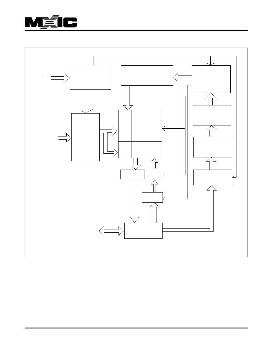
Commands are written to the command register using
standard microprocessor write timings. Register con-
tents serve as inputs to an internal state-machine
which controls the erase and programming circuitry.
During write cycles, the command register internally
latches address and data needed for the programming
and erase operations. For system design simplifica-
tion, the MX28F2000T is designed to support either
WE or CE controlled writes. During a system write
cycle, addresses are latched on the falling edge of WE
or CE whichever occurs last. Data is latched on the
rising edge of WE or CE whichever occur first. To
simplify the following discussion, the WE pin is used as
the write cycle control pin throughout the rest of this
text. All setup and hold times are with respect to the
WE signal.
MXIC's Flash technology combines years of EPROM
experience to produce the highest levels of quality, relia-
bility, and cost effectiveness. The MX28F2000P electri-
cally erases all bits simultaneously using Fowler-Nord-
heim tunneling. The bytes are programmed one byte at
a time using the EPROM programming mechanism of hot
electron injection.
AUTOMATIC ERASE ALGORITHM