GENERAL DESCRIPTION
The MX28F2100B is a 2-mega bit Flash memory or-
ganized as 256K bytes of 8 bits or 128K words of 16
bits switchable. MXIC's Flash memories offer the
most cost-effective and reliable read/write non-
volatile random access memory. The MX28F2100B
is packaged in 44-pin SOP and 48-pin TSOP
(I
). It is
designed to be reprogrammed and erased in-system
or in-standard EPROM programmers.
The standard MX28F2100B offers access times as
fast as 70ns, allowing operation of high-speed
microprocessors without wait states. To eliminate
bus contention, the MX28F2100B has separate chip
enable (CE) and output enable (OE ) controls.
MXIC's Flash memories augment EPROM function-
a l i t y w i t h i n - c i r c u i t e l e c t r i c a l e r a s u r e a n d
programming. The MX28F2100B uses a command
register to manage this functionality. The command
register allows for 100% TTL level control inputs and
f i x e d p o w e r s u p p l y l e v e l s d u r i n g e r a s e a n d
programming, while maintaining maximum EPROM
compatibility.
MXIC Flash technology reliably stores memory con-
tents even after 10,000 erase and program cycles.
The MXIC cell is designed to optimize the erase and
programming mechanisms. In addition, the combi-
nation of advanced tunnel oxide processing and low
internal electric fields for erase and programming
o p e r a t i o n s p r o d u c e s r e l i a b l e c y c l i n g . T h e
MX28F2100B uses a 12.0V
±
7% VPP supply to
FEATURES
∑ 262,144x8/131,072x16 switchable
∑ Fast access time: 70/90/120ns
∑ Low power consumption
≠ 50mA maximum active current
≠ 100uA maximum standby current
∑ Programming and erasing voltage 12V
±
7%
∑ Command register architecture
≠ Byte/Word Programming (50 us typical)
≠ Auto chip erase 5 sec typical
(including preprogramming time)
≠ Block Erase (Any one from 5 blocks:16K-Byte x1,
8K-Byte x2, 96K-Byte x1, and 128K-Byte x1)
≠ Auto Erase with Erase Suspend capability
1
∑ Status Register feature for Device status detection
∑ Auto Erase (chip & block) and Auto Program
≠ Status Registers
∑ 10,000 minimum erase/program cycles
∑ Latch-up protected to 100mA from -1 to VCC+1V
∑ Package type:
≠ 44-pin SOP
≠ 48-pin TSOP (Type 1)
perform the High Reliability Erase and auto Program/
Erase algorithms.
The highest degree of latch-up protection is
achieved with MXIC's proprietary non-epi process.
Latch-up protection is proved for stresses up to 100
milliamps on address and data pin from -1V to VCC
+ 1V.
P/N: PM0382
REV. 1.5, MAR. 24, 1998
BLOCK STRUCTURE
1 F F F F H
1 6 K - B Y T E B L O C K
A 1 6 ~ A 0
8 K - B Y T E B L O C K
8 K - B Y T E B L O C K
9 6 K - B Y T E B L O C K
1 0 0 0 0 H
0 F F F F H
0 4 0 0 0 H
0 3 F F F H
0 3 0 0 0 H
0 2 F F F H
0 2 0 0 0 H
0 1 F F F H
1 2 8 K - B Y T E B L O C K
0 0 0 0 0 H
Wo r d M o d e ( x 1 6 ) M e m o r y M a p
* B y t e M o d e o p e ra t i o n s h o u l d i n c l u d e
A - 1 ( L S B ) fo r a d d r e s s i n g
PRELIMINARY
MX28F2100B
2M-BIT [256K x 8/128K x 16] CMOS FLASH MEMORY
2
MX28F2100B
P/N: PM0382
REV. 1.5, MAR. 24, 1998
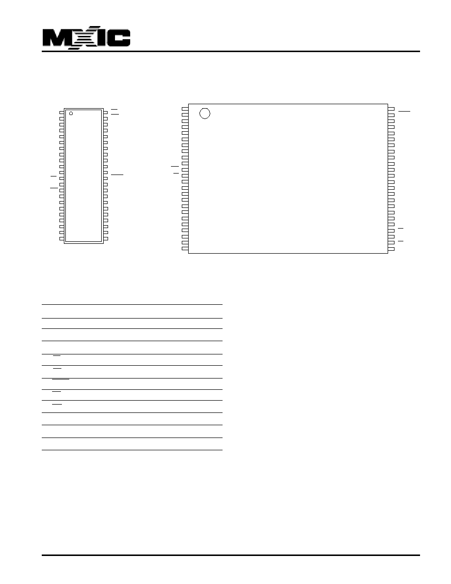
PIN CONFIGURATIONS
44 SOP(500 mil)
TSOP (TYPE 1) (12mm x 20mm)
(NORMAL TYPE)
SYMBOL
PIN NAME
A0~A16
Address Input
Q0~Q14
Data Input/Output
Q15/A-1
Q15(Word mode)/LSB addr(Byte mode)
CE
Chip Enable Input
WE
Write Enable Input
BYTE
Word/Byte Selction input
RP
Reset/Deep Power Down
OE
Output Enable Input
VPP
Power supply for Program and Erase
VCC
Power Supply Pin (+5V)
GND
Ground Pin
PIN DESCRIPTION:
2
3
4
5
6
7
8
9
10
11
12
13
14
15
16
17
18
19
20
21
22
44
43
42
41
40
39
38
37
36
35
34
33
32
31
30
29
28
27
26
25
24
23
VPP
NC
NC
A7
A6
A5
A4
A3
A2
A1
A0
CE
GND
OE
Q0
Q8
Q1
Q9
Q2
Q10
Q3
Q11
RP
WE
A8
A9
A10
A11
A12
A13
A14
A15
A16
BYTE
GND
Q15/A-1
Q7
Q14
Q6
Q13
Q5
Q12
Q4
VCC
MX28F2100B
A15
A14
A13
A12
A11
A10
A9
A8
NC
NC
WE
RP
VPP
NC
NC
NC
NC
A7
A6
A5
A4
A3
A2
A1
1
2
3
4
5
6
7
8
9
10
11
12
13
14
15
16
17
18
19
20
21
22
23
24
A16
BYTE
GND
Q15/A-1
Q7
Q14
Q6
Q13
Q5
Q12
Q4
VCC
Q11
Q3
Q10
Q2
Q9
Q1
Q8
Q0
OE
GND
CE
A0
48
47
46
45
44
43
42
41
40
39
38
37
36
35
34
33
32
31
30
29
28
27
26
25
MX28F2100B
3
MX28F2100B
P/N: PM0382
REV. 1.5, MAR. 24, 1998
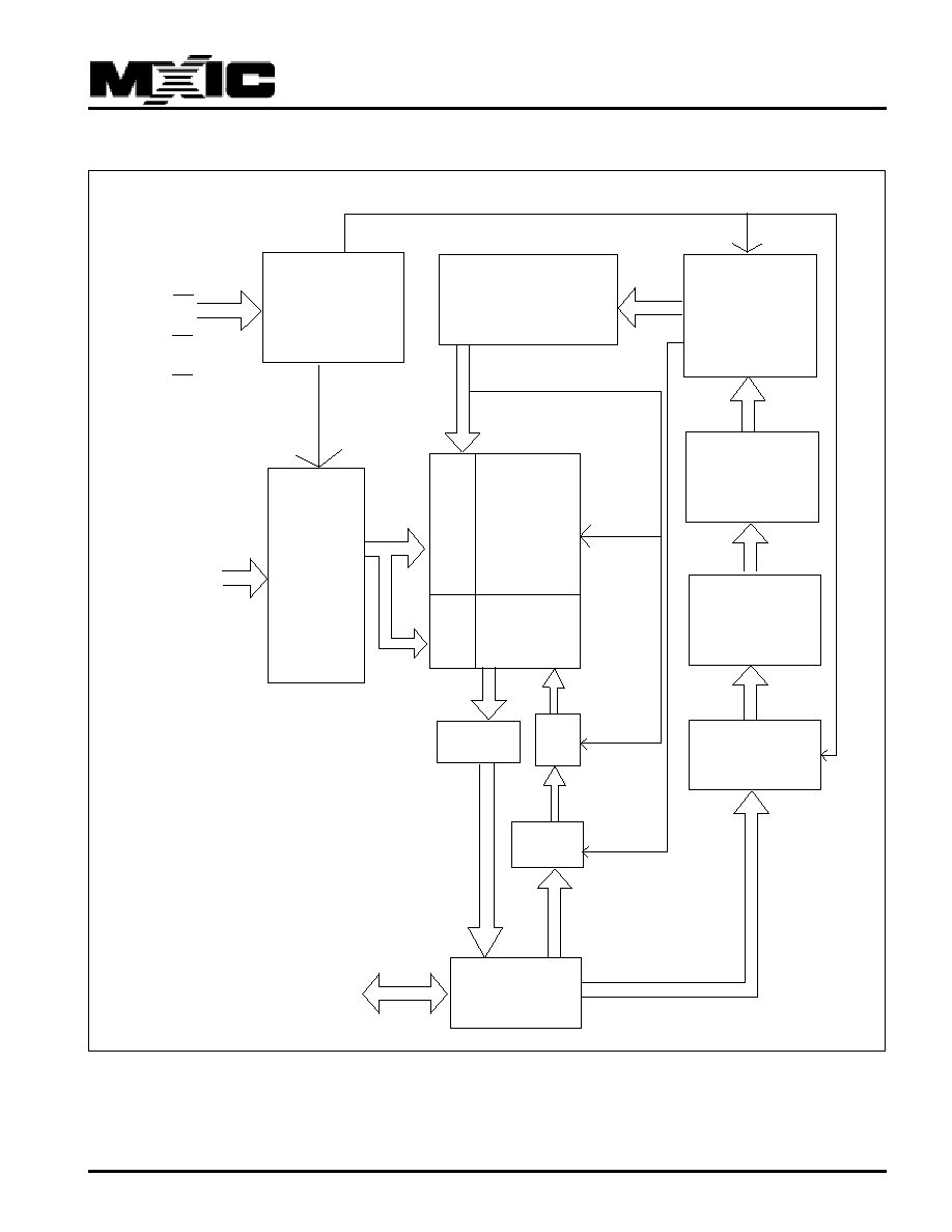
BLOCK DIAGRAM
CONTROL
INPUT
LOGIC
PROGRAM/ERASE
HIGH VOLTAGE
WRITE
STATE
MACHINE
(WSM)
STATE
REGISTER
MX28F2100B
FLASH
ARRAY
X-DECODER
ADDRESS
LATCH
AND
BUFFER
Y-PASS GATE
Y
-DECODER
ARRAY
SOURCE
HV
COMMAND
DATA
DECODER
COMMAND
DATA LATCH
I/O BUFFER
PGM
DATA
HV
PROGRAM
DATA LATCH
SENSE
AMPLIFIER
Q0-Q15/A-1
Q15/A-1
A0-A16
CE
OE
WE
BYTE
RP

4
MX28F2100B
P/N: PM0382
REV. 1.5, MAR. 24, 1998
AUTOMATIC PROGRAMMING
The MX28F2100B is byte/word programmable using
the Automatic Programming algorithm. The Automatic
Programming algorithm does not require the system to
time out or verify the data programmed. The typical
room temperature chip programming time of the
MX28F2100B is less than 5 seconds.
AUTOMATIC CHIP ERASE
The entire chip is bulk erased using 10 ms erase
pulses according to MXIC's High Reliability Chip Erase
algorithm. Typical erasure at room temperature is
accomplished in less than five seconds. The device
may also be erased using the Automatic Erase
algorithm. The Automatic Erase algorithm automati-
cally programs the entire array prior to electrical erase.
The timing and verification of electrical erase are
controlled internally.
AUTOMATIC BLOCK ERASE
The MX28F2100B is block(s) erasable using MXIC's
Auto Block Erase algorithm. Block erase modes allow
one of 5 blocks of the array to be erased in one erase
cycle. The Automatic Block Erase algorithm automati-
cally programs the specified block(s) prior to electrical
erase. The timing and verification of electrical erase
are controlled internal to the device.
AUTOMATIC PROGRAMMING ALGORITHM
MXIC's Automatic Programming algorithm requires
the user to only write a program set-up command and
a program command (program data and address). The
device automatically times the programming pulse
width, provides the program verify, and counts the
number of sequences. A status register scheme pro-
vides feedback to the user as to the status of the
programming operation.
MXIC's Automatic Erase algorithm requires the user to
only write an Erase Set-up command and an Erase
command. The device will automatically pre-program
and verify the entire array. Then the device automati-
cally times the erase pulse width, provides the erase
verify, and counts the number of sequences. A status
register provides feedback to the user as to the status
of the erase operation. It is noted that after an Erase
Set-up command, if the next command is not an Erase
command, then the state-machine will set both the
program status and Erase Status bits of the Status
Register to a "1", place the device into the read Status
Register state, and wait for another command.
Commands are written to the command register using
standard microprocessor write timings. Register con-
tents serve as inputs to an internal state-machine
which controls the erase and programming circuitry.
During write cycles, the command register internally
latches address and data needed for the programming
and erase operations. During a system write cycle,
addresses are latched on the falling edge, and data is
latched on the rising edge of WE .
MXIC's Flash technology combines years of EPROM
experience to produce the highest levels of quality, relia-
bility, and cost effectiveness. The MX28F2100B electri-
cally erases all bits within a sector or chip simultaneously
using Fowler-Nordheim tunneling. The array is pro-
grammed one byte/word at a time using the EPROM
programming mechanism of hot electron injection.
During a program cycle, the state-machine will control the
program sequences and command register will not re-
spond to any command set. During a Sector/Chip Erase
cycle, the command register will respond to Erase Sus-
pend command. After Erase Suspend completed, the
device stays at status register Read state. After the state
machine has completed its task, it will allow the command
register to respond to its full command set.
AUTOMATIC ERASE ALGORITHM
5
MX28F2100B
P/N: PM0382
REV. 1.5, MAR. 24, 1998
TABLE 1. SOFTWARE COMMAND DEFINITIONS
COMMAND
BUS
FIRST BUS CYCLE
SECOND BUS CYCLE
CYCLE
Mode
Address Data
Mode
Address Data
X8
X16
X8
X16
Read Memory Array
1
Write
X
FFH
XXFFH
---
---
---
---
Setup Auto program/
2
Write
X
10H
XX10H
Write
Program Program Program
Auto Program
or 40H
or XX40H
Address
Data
Data
Setup Erase/Erase(Chip)
2
Write
X
20H
XX20H
Write
X
20H
XX20H
Setup Erase/Erase(Block)
2
Write
X
60H
XX60H
Write
Block
60H
XX60H
Address
Setup Auto Erase/
2
Write
X
30H
XX30H
Write
X
30H
XX30H
Auto Erase(Chip)
Setup Auto Erase/
2
Write
X
20H
XX20H
Write
Block
D0H
XXD0H
Auto Erase(Block)
Address
Erase Verify
2
Write
Verify
A0H
XXA0H
Read
X
Verify
Verify
Address
Data
Data
Read device identifier code
2
Write
X
90H
XX90H
Read
ADI
DDI
DDI
Erase Suspend
1
Write
X
B0H
XXB0H
---
---
---
---
Erase Resume
1
Write
X
D0H
XXD0H
---
---
---
---
Read Status Register
2
Write
X
70H
XX70H
Read
X
SRD
SRD
Clear Status Register
1
Write
X
50H
XX50H
---
---
---
---
COMMAND DEFINITIONS
Placing high voltage on the VPP pin enables read/write
operations. Device operations are selected by writing
specific data patterns into the command register. Ta-
ble 1 defines these MX28F2100B register commands.
Table 2 defines the bus operations of MX28F2100B.
Note:
1. Write and Read mode are defined in mode selection table.
2. ADI = Address of Device identifier; A0 = 0 for manufacture code, A0 = 1 for device code.
DDI = Data of Device identifier : C2H for manufacture code, 2BH for device code(Byte = VIL) ; 00C2H for
manufacture code, 002BH for device code(Byte =VIH)
X = X can be VIL or VIH
SRD = Status Register Data
6
MX28F2100B
P/N: PM0382
REV. 1.5, MAR. 24, 1998
TABLE 2. MX28F2100B BUS OPERATION
Pins
A0
A9
CE
OE
WE
VPP
Data I/O
Mode
D0~D7
D8~D14
D15/A-1
Read
A0
A9
VIL
VIL
VIH
VPPL
Data Out
Hi-Z
A-1
Output Disable
X
X
VIL
VIH VIH
VPPL
Hi-Z
Hi-Z
X
Byte
Read-Only
Standby
X
X
VIH
X
X
VPPL
Hi-Z
Hi-Z
X
Mode
Read Silicon ID(Mfr)(2)
VIL
VID(3) VIL
VIL
VIH
VPPL
Data=C2H
Hi-Z
VIL
BYTE
Read Silicon ID(Device)(2) VIH VID(3) VIL
VIL
VIH
VPPL
Data=2BH
Hi-Z
VIL
= L
Read
A0
A9
VIL
VIL
VIH
VPPH Data Out(4)
Hi-Z
A-1
Read/Write Output Disable
X
X
VIL
VIH VIH
VPPH
Hi-Z
Hi-Z
X
Standby(5)
X
X
VIH
X
X
VPPH
Hi-Z
Hi-Z
X
Write
A0
A9
VIL
VIH
VIL
VPPH
Data In(6)
X
A-1
Read
A0
A9
VIL
VIL
VIH
VPPL
Data Out
Data Out
Data Out
Read-Only
Output Disable
X
X
VIL
VIH VIH
VPPL
Hi-Z
Hi-Z
Hi-Z
Word
Standby
X
X
VIH
X
X
VPPL
Hi-Z
Hi-Z
Hi-Z
Mode
Read Silicon ID(Mfr)(2)
VIL
VID(3) VIL
VIL
VIH
VPPL
Data=C2H Data=00H(8)
0B
BYTE
Read Silicon ID(Device)(2) VIH VID(3) VIL
VIL
VIH
VPPL
Data=2BH Data=00H(8)
0B
= H
Read
A0
A9
VIL
VIL
VIH
VPPH Data Out(4)
Data Out
Data Out
Read/Write Output Disable
X
X
VIL
VIH VIH
VPPH
Hi-Z
Hi-Z
Hi-Z
Standby(5)
X
X
VIH
X
X
VPPH
Hi-Z
Hi-Z
Hi-Z
Write
A0
A9
VIL
VIH
VIL
VPPH
Data In(6)
Data In(6) Data In(6)
NOTES:
1. VPPL may be grounded, a no-connect with a resistor tied
to ground, or < VCC + 2.0V. VPPH is the programming
voltage specified for the device. When VPP = VPPL,
memory contents can be read but not written or erased.
2. Manufacturer and device codes may also be accessed
via a command register write sequence. Refer to Table
1. All other addresses are low.
3. VID is the Silicon-ID-Read high voltage, 11.5V to 13V.
4. Read operations with VPP = VPPH may access array
data or Silicon ID codes.
5. With VPP at high voltage, the standby current equals ICC
+ IPP (standby).
6. Refer to Table 1 for valid Data-In during a write operation.
7. X can be VIL or VIH.
8. Includes D15
Pins
A0 D15 D14 D13 D12 D11 D10 D9
D8 D7 D6 D5 D4 D3 D2 D1 D0
Code(Hex)
Code
BYTE
Manufacture code
VIL VIL
---
---
---
---
---
---
---
1
1
0
0
0
0
1
0
C2H
= L
Device code
VIH VIL
---
---
---
---
---
---
---
0
0
1
0
1
0
1
1
2BH
BYTE
Manufacture code
VIL
0
0
0
0
0
0
0
0
1
1
0
0
0
0
1
0
00C2H
= H
Device code
VIH
0
0
0
0
0
0
0
0
0
0
1
0
1
0
1
1
002BH
TABLE 3. SILICON ID CODE

7
MX28F2100B
P/N: PM0382
REV. 1.5, MAR. 24, 1998
ERASE-VERIFY COMMAND
After each erase operation, all bytes must be verified.
The Erase Verify operation is initiated by writing
XXA0H into the command register. The address for
the byte to be verified must be supplied as it is latched
on the falling edge of the WE pulse.
The MX28F2100B applies an internally generated
margin voltage to the addressed byte. Reading
FFFFH from the addressed byte indicates that all bits
in the byte are erased.
The Erase-Verify command must be written to the
command register prior to each byte verification to
latch its address. The process continues for each byte
in the array until a byte does not return FFFFH data, or
the last address is accessed.
In the case where the data read is not FFFFH, another
erase operation needs to be performed. (Refer to Set-
up Erase/Erase). Verification then resumes from the
address of the last-verified byte. Once all bytes in the
array have been verified, the erase step is complete.
The device can be programmed. At this point, the
verify operation is terminated by writing a valid
command (e.g. Program Set-up) to the command
register. The High Reliability Erase algorithm
illustrates how commands and bus operations are
combined to perform electrical erasure of the
MX28F2100B.
SET-UP AUTOMATIC CHIP ERASE/ERASE
COMMANDS
The Automatic Chip Erase does not require the device
to be entirely pre-programmed prior to excuting the
Automatic Set-up Erase command and Automatic Chip
Erase command. Upon executing the Automatic Chip
Erase command, the device automatically will
program and verify the entire memory for an all-zero
data pattern. When the device is automatically verified
to contain an all-zero pattern, a self-timed chip erase
and verify begin. The erase and verify operations are
completed by the feed back of the status register. The
system is not required to provide any control or timing
during these operations.
READ COMMAND
While V
PP
is high, for erasure and programming,
memory contents can also be accessed via the Read
command. The read operation is initiated by writing
XXFFH into the command register. Microprocessor
read cycles retrieve array data. The device remains
enabled for reads until the command register contents
are altered.
RESET COMMAND
A Reset command is provided as a means to safely
abort the erase- or program-command sequences.
Following Set-up command with two consecutive
writes of XXFFH for ERS (or one write of XXFFH for
PGM) will safely abort the operation. Memory contents
will not be altered. A valid command must then be
written to place the device in the desired state.
SILICON-ID-READ COMMAND
Flash-memories are intended for use in applications
where the local CPU alters memory contents. As such,
manufacturer- and device-codes must be accessible
while the device resides in the target system. PROM
programmers typically access signature codes by rais-
ing A9 to a high voltage. However, multiplexing high
voltage onto address lines is not a desired system-
design practice.
The MX28F2100B contains a Silicon-ID-Read
o p e r a t i o n t o s u p p l e m e n t t r a d i t i o n a l P R O M -
programming methodology. The operation is initiated
by writing XX90H into the command register.
Following the command write, a read cycle with
A 0 = V I L r e t r i e v e s t h e m a n u f a c t u r e r c o d e o f
C2H(BYTE=VIL, 00C2H(BYTE=VIH). A read cycle
with A0=VIH returns the device code of 2BH(BYTE =
VIL), 002BH(BYTE = VIH).

8
MX28F2100B
P/N: PM0382
REV. 1.5, MAR. 24, 1998
When using the Automatic Chip Erase algorithm, note
that the erase automatically terminates when
adequate erase margin has been achieved for the
memory array(no erase verify command is required).
The margin voltages are internally generated in the
same manner as when the standard Erase Verify
command is used.
If the Erase operation was unsuccessful, bit 5 of the
Status Register will be set to a "1", indicating an Erase
Failure. If Vpp was not within acceptable limits after
the Erase command is issued, the state machine will
not execute an erase sequence; in stead, bit 5 of the
Status Register is set to a "1" to indicate an Erase
Failure, and bit 3 is set to a "1" to indentify that Vpp
supply voltage was not within acceptable limits.
The Automatic Set-up Erase command is a command
only operation that stages the device for automatic
electrical erasure of all bytes in the array. Automatic
set-up erase is performed by writing XX30H to the
command register.
To commence Automatic Chip Erase, the command
XX30H must be written again to the command register.
SET-UP AUTOMATIC BLOCK ERASE/ERASE
COMMANDS
The Automatic Block Erase does not require the device
to be entirely pre-programmed prior to executing the
Automatic Set-up Block Erase command and
Automatic Block Erase command. Upon executing the
Automatic Block Erase command, the device
automatically will program and verify the block(s)
memory for an all-zero data pattern. The system is not
required to provide any controls or timing during these
operations.
When the block(s) is automatically verified to contain
an all-zero pattern, a self-timed block erase and verify
begin. The system is not required to provide any
control or timing during these operations.
When using the Automatic Block Erase algorithm, note
that the erase automatically terminates when adequate
erase margin has been achieved for the memory array
(no erase verify command is required). The margin
voltages are internally generated in the same manner
as when the standard Erase Verify command is used.
The Automatic Set-up Block Erase command is a com-
mand only operation that stages the device for auto-
matic electrical erasure of selected blocks in the array.
Automatic Set-up Block Erase is performed by writing
XX20H to the command register. To enter Automatic
Block Erase, the user must write the command D0H to
the command register. Block addresses selected are
loaded into internal register on the second falling edge
of WE. Each successive block load cycle started by the
falling edge of WE must begin within 30us from the
rising edge of the preceding WE. Otherwise, the
loading period ends and internal auto block erase cycle
starts.
ERASE SUSPEND
This command only has meaning while the state ma-
chine is executing Automatic Chip/Block Erase opera-
tion, and therefore will only be responded to during
Automatic Chip/Block Erase operation. It is noted that
Erase Suspend is meaningful for block erase only after
block addresses load are finished (100 us after the last
address is loaded). After this command has been ex-
ecuted, the command register will initiate erase sus-
pend mode. The state machine will set DQ7, DQ6 as 1,
1, after suspend is ready. At this time, state machine
only allows the command register to respond to the
Read Memory Array, Erase Resume and Read Status
Register.

9
MX28F2100B
P/N: PM0382
REV. 1.5, MAR. 24, 1998
SET-UP AUTOMATIC PROGRAM/PROGRAM
COMMANDS
The Automatic Set-up Program is a command only
operation that stages the device for automatic pro-
gramming. Automatic Set-up Program is performed by
writing XX10H/XX40H to the command register.
Program command is the command for byte-program
or word-program.
Once the Automatic Set-up Program operation is per-
formed, the next WE pulse causes a transition to an
active programming operation. Addresses are latched
on the falling edge, and data are internally latched on
the rising edge of the WE pulse. The rising edge of WE
also begins the programming operation. The system is
not required to provide further controls or timings. The
device will automatically provide an adequate
internally generated program pulse and verify margin.
If the program opetation was unsuccessful, bit 4 of the
Status Register will be set to a "1", indicating a
program failure. If Vpp was not within acceptable limits
after the program command is issued, the state
machine will not execute a program sequence; in
stead, bit 4 of the Status Register is set to a "1" to
indicate a Program Failure, and bit 3 is set to a "1" to
identify that Vpp supply voltage was not within
acceptable limits.
STATUS REGISTER
The device contains a Status Register which may be
read to determine when a Program or Erase operation
is complete, and whether that operation completed
successfully. The Status Register may be read at any
time by writing the Read Status command to the
command interface. After writing this command, all
subsequent Read operations output data from the
Status Register until another command is written to the
command interface. A Read Array command must be
written to the command interface to return to the read
array mode.
ERASE RESUME
This command will cause the command register to clear
the suspend state and set DQ6, DQ7, back to 0, 0, but
only if an Erase Suspend command was previously
issued. Erase Resume will not have any effect in all other
conditions.
The Status Register bits are output on DQ[0:7],
whether the device is in the byte-wide (x8) or word-
wide (x16) mode. In the word-wide mode the upper
byte, DQ[8:15], is set to 00H during a Read Status
command. In the byte-wide mode, DQ[8:14] are tri-
stated and DQ15/A-1 retains the low order address
function.
The contents of the Status Register are latched on the
falling edge of OE or CE, whichever occurs last in the
read cycle. This prevents possible bus errors which
might occur if the contents of the Status Register
change while reading the Status Register. CE or OE
must be toggled with each subsequent status read, or
the completion of a Program or Erase operation will not
be evident from the Status Register.
When the state machine is active, this register will
indicate the status of the state machine, and will also
hold the bits indicating whether or not the state
machine was successful in performing the desired
operation.
CLEARING THE STATUS REGISTER
The state machine sets status bits "3" through "7" to
"1", and clears bits "6" and "7" to "0", but cannot clear
status bits "3" through "5" to "0". Bits 3 through 5 can
only be cleared by the controlling CPU through the use
of the Clear Status Register command. These bits can
indicate various error conditions. By allowing the
system software to control the resetting of these bits,
several operations may be performed (such as
cumulatively programming several bytes or erasing
multiple blocks in sequence). The Status Register may
then be read to determine if an error occurred during
that programming or erasure series. This adds
flexibility to the way the device may be programmed or
erased. Once an error occured, the command
Interface Only responds to clear Status Register, Read
Status Register and Read Array. To clear the Status
Register, the Clear Status Register command is written
to the command interface. Then, any other command
may be issued to the command interface. Note, again,
that before read cycle can be initiated, a Read Array
command must be written to the command interface to
specify whether the read data is to come from the
Memory Array, Status Register, or Sili-con -ID.

10
MX28F2100B
P/N: PM0382
REV. 1.5, MAR. 24, 1998
Status Register Bit Definition
SR.7 = WRITE STATE MACHINE STATUS(WSMS)
1 = Ready
0 = Busy
SR.6 = ERASE-SUSPEND STATUS (ESS)
1 = Erase Suspended
0 = Erase in Progress/Completed
SR.5 = ERASE STATUS
1 = Error in Erase
0 = Successful Erasure
SR.4 = PROGRAM STATUS
1 = Error in Byte/Word Program
0 = Successful Byte/Word Program
SR.3 = Vpp STATUS
1 = Vpp Low Detect, Operation Abort
0 = Vpp OK
NOTE :
State machine bit must first be checked to determine
Byte/Word program or Block Erase completion, before
the Program or Erase Status bits are checked for success.
When Erase Suspend is issued, state machine halts
execution and sets both WSMS and ESS bits to "1," ESS
bit remains set to "1" until an Erase Resume command is
issued.
When this bit set to "1," state machine has applied the
maximum number of erase pulses to the device and is still
unable to successfully verify erasure.
When this bit is set to "1," state machine has attempted
but failed to program a byte or word.
The Vpp status bit, unlike an A/D converter, does not
provide continuous indication of Vpp level. The state
machine interrogates Vpp level only after the Byte Write
or Erase command sequences have been entered, and
informs the system if Vpp has not been switched on.
WSMS
ESS
ES
PS
VPPS
7
6
5
4
3

11
MX28F2100B
P/N: PM0382
REV. 1.5, MAR. 24, 1998
DATA PROTECTION
The MX28F2100B is designed to offer protection against
accidental erasure or programming caused by spurious
system level signals that may exist during power transition.
During power up the device automatically resets the state
machine in the Read mode. In addition, with its control
register architecture, alteration of the memory contents
only occurs after successful completion of specific
command sequences. The device also incorporates
several features to prevent inadvertent write cycles
resulting from VCC power-up and power-down transition
or system noise.
LOW VPP WRITE INHIBIT
To avoid initiation of a write cycle during V
PP
power-up
and power-down a write cycle is locked out for V
PP
less
than V
PPLK
(typically 9V). If V
PP
< V
PPLK
, the command
register is disabled and all internal program/erase circuits
are disabled. Subsequent writes will be ignored until the
V
PP
level is greater than V
PPLK
. It is the user's responsibility
to ensure that the control pins are logically correct to
prevent unintentional write when V
PP
is above V
PPLK
.
LOGICAL INHIBIT
Writing is inhibited by holding any one of OE = VIL, CE =
VIH or WE = VIH. To initiate a write cycle CE and WE must
be a logical zero while OE is a logical one.
POWER SUPPLY DECOUPLING
In order to reduced power switching effect, each device
should have a 0.1uF ceramic capacitor connected between
its VCC and GND, and between its VPP and GND.
VPP TRACE ON PRINTED CIRCUIT BOARD
Programming flash memories, while they reside in the
target system, requires that the printed circuit board
designer pay attention to the Vpp power supply trace.
The Vpp pin supplies the memory cell current for
programming. Use similar trace widths and layout
considerations given to the Vcc power bus. Adequate
Vpp supply traces and decoupling will decrease Vpp
voltage spikes and overshoots.
DEEP POWER DOWN MODE
This mode is enabled by RP pin. During Read modes, RP
going low deselects the memory and place the output
drivers in a high-Z state.
In erase or program modes, RP low will abort erase or
program operations, but the memory contents are no
longer valid as the data has been corrupted by RP
function. RP transition to VIL, or turning power off to the
device will clear up Status Register and automatically
defaults to the read array mode.
POWER-UP SEQUENCE
The MX28F2100B powers up in the Read only mode. In
addition, the memory contents may only be altered after
successful completion of a two-step command sequence.
Vpp and Vcc power up sequence is not required.
WRITE PULSE "GLITCH" PROTECTION
Noise pulses of less than 5ns(typical) on CE or WE will not
initiate a write cycle.
12
MX28F2100B
P/N: PM0382
REV. 1.5, MAR. 24, 1998
ABSOLUTE MAXIMUM RATINGS
RATING
VALUE
Ambient Operating Temperature
0
o
C to 70
o
C
Storage Temperature
-65
o
C to 125
o
C
Applied Input Voltage
-0.5V to 7.0V
Applied Output Voltage
-0.5V to 7.0V
VCC to Ground Potential
-0.5V to 7.0V
A9 & VPP & RP
-0.5V to 13.5V
NOTICE:
Stresses greater than those listed under ABSOLUTE MAXI-
MUM RATINGS may cause permanent damage to the de-
vice. This is a stress rating only and functional operational
sections of this specification is not implied. Exposure to ab-
solute maximum rating conditions for extended period may
affect reliability.
NOTICE:
Specifications contained within the following tables are sub-
ject to change.
SWITCHING VCC VOLTAGES
VCC SUPPLY SWITCHING TIMING
SYMBOL
PARAMETER
MIN.
MAX.
UNIT
T5VPH
VCC at 4.5V (minimum) to RP High
3
ms
NOTICE:
The T5VPH time must be strictly followed to guarantee all
other read and write specifications.
VCC SUPPLY SWITCHING WAVEFORM
CAPACITANCE TA = 25
o
C, f = 1.0 MHz
SYMBOL
PARAMETER
MIN.
TYP
MAX.
UNIT
CONDITIONS
CIN
Input Capacitance
8
pF
VIN = 0V
COUT
Output Capacitance
12
pF
VOUT = 0V
t5VPH
5.0V
VCC
GND
VIH
RP
VIL
13
MX28F2100B
P/N: PM0382
REV. 1.5, MAR. 24, 1998
READ OPERATION
DC CHARACTERISTICS
TA = 0
o
C TO 70
o
C, VCC = 5V
±
10%, VPP = GND to VCC
SYMBOL
PARAMETER
MIN.
TYP
MAX.
UNIT
CONDITIONS
ILI
Input Leakage Current
1
uA
VIN = GND to VCC
ILO
Output Leakage Current
10
uA
VOUT = GND to VCC
IPP1
VPP Current
1
100
uA
VPP = 5.5V
ISB1
Standby VCC current
1
mA
CE = VIH
ISB2
1
100
uA
CE = VCC + 0.3V
ICC1
Operating VCC current
50
mA
IOUT = 0mA, f=1MHz
ICC2
70
mA
IOUT = 0mA, f=10MHz
VIL
Input Low Voltage
-0.3
(NOTE 1)
0.8
V
VIH
Input High Voltage
2.0
VCC + 0.3
V
VOL
Output Low Voltage
0.45
V
IOL = 2.1mA
VOH
Output High Voltage
2.4
V
IOH = -400uA
NOTES:
1. VIL min. = -1.0V for pulse width < 50 ns.
VIL min. = -2.0V for pulse width < 20 ns.
2. VIH max. = VCC + 1.5V for pulse width < 20 ns
If VIH is over the specified maximum value, read operation
cannot be guaranteed.
AC CHARACTERISTICS
TA = 0
o
C to 70
o
C, VCC = 5V
±
10%, VPP = GND to VCC
28F2100B-70
28F2100B-90 28F2100B-12
SYMBOL
PARAMETER
MIN.
MAX.
MIN.
MAX.
MIN.
MAX.
UNIT
CONDITIONS
tACC
Address to Output Delay
70
90
120
ns
CE=OE=VIL
tCE
CE to Output Delay
70
90
120
ns
OE=VIL
tOE
OE to Output Delay
30
40
50
ns
CE=VIL
tDF
OE High to Output Float
(
Note1)
0
20
0
30
0
30
ns
CE=VIL
tOH
Address to Output hold
0
0
0
ns
CE=OE=VIL
NOTE:
1. tDF is defined as the time at which the output achieves the
open circuit condition and data is no longer driven.
TEST CONDITIONS:
∑ Input pulse levels: 0.45V/2.4V
∑ Input rise and fall times: < 10ns
∑ Output load: 1 TTL gate + 35pF (Including scope and jig)
∑ Reference levels for measuring timing: 0.8V, 2.0V
14
MX28F2100B
P/N: PM0382
REV. 1.5, MAR. 24, 1998
BYTE READ TIMING WAVEFORMS
WORD READ TIMING WAVEFORMS
A-1~16
CE
OE
tACC
WE
VIH
VIL
VIH
VIL
VIH
VIL
VIH
VIL
VIH
VIL
VOH
VOL
HIGH Z
HIGH Z
DATA Valid
tOE
tDF
tCE
BYTE
DATA
Q0~7
HIGH Z
HIGH Z
VOH
VOL
DATA
Q8~14
tOH
ADD Valid
RP
A0-16
CE
OE
tACC
WE
VIH
VIL
VIH
VIL
VIH
VIL
VIH
VIL
VIH
VIL
VOH
VOL
STANDBY MODE
STANDBY MODE
HIGH Z
HIGH Z
DATA VALID
tOE
tDF
tCE
tOH
BYTE
DATA
Q0-15
ACTIVE MODE
ADD VALID
RP

15
MX28F2100B
P/N: PM0382
REV. 1.5, MAR. 24, 1998
DC CHARACTERISTICS
TA = 0
o
C to 70
o
C, VCC = 5V
±
10%, VPP = 12V
±
7%
SYMBOL
PARAMETER
MIN.
TYP
MAX.
UNIT
CONDITIONS
ILI
Input Leakage Current
1
uA
VIN=GND to VCC
ILO
Output Leakage Current
10
uA
VOUT=GND to VCC
ISB1
Standby VCC current
1
mA
CE=VIH
ISB2
1
100
uA
CE=VCC
±
0.3V
ICC1 (Read)
Operating VCC Current
50
mA
IOUT=0mA, f=1MHz
ICC2
70
mA
IOUT=0mA, F=10MHz
ICC3 (Program)
50
mA
In Programming
ICC4 (Erase)
50
mA
In Erase
ICCES
VCC Erase Suspend Current
10
mA
CE=VIH, Erase Suspended
IPP1 (Read)
VPP Current
200
uA
VPP=12.8V
IPP2 (Program)
50
mA
In Programming
IPP3 (Erase)
50
mA
In Erase
VIL
Input Voltage
-0.3 (Note 5)
0.8
V
VIH
2.0
VCC+0.3V V
(Note 6)
VOL
Output Voltage
0.45
V
IOL=2.1mA
VOH
2.4
V
IOH=-400uA
VPPLK
VPP Lockout Voltage
0.0
6
V
VPPH
VPP for Program/Erase Operation 11.16
12.84
V
12V
±
7%
COMMAND PROGRAMMING/DATA PROGRAMMING/ERASE OPERATION
NOTES:
1. VCC must be applied before VPP and remove after VPP.
2. VPP must not exceed 14V including overshoot.
3. An influence may be had upon device reliability if the device
is installed or removed while VPP=12V.
4. Do not alter VPP either VIL to 12V or 12V to VIL when
CE=VIL.
5. VIL min. = -0.6V for pulse width < 20ns.
6. If VIH is over the specified maximum value, programming
operation cannot be guranteed.
7. ICCES is specified with the device de-selected. If the device
is read during erase suspend mode, current draw is the sum
of ICCES and ICC1 or ICC2.
8. All current are in RMS unless otherwisw noted.
16
MX28F2100B
P/N: PM0382
REV. 1.5, MAR. 24, 1998
AC CHARACTERISTICS
TA = 0
o
C to 70
o
C, VCC = 5V
±
10%, VPP =12V
±
7%
28F2100B-70 28F2100B-90 28F2100B-12
SYMBOL
PARAMETER
MIN.
MAX.
MIN.
MAX. MIN.
MAX. UNIT CONDITIONS
tVPS
VPP setup time
100
100
100
ns
tPHEL
1000
1000
1000
ns
tOES
OE setup time
100
100
100
ns
tCWC
Command programming cycle
70
90
120
ns
tCEP
WE programming pulse width
50
50
50
ns
tCEPH1
WE programming pluse width High
20
20
20
ns
tCEPH2
WE programming pluse width High
100
100
100
ns
tAS
Address setup time
0
0
0
ns
tAH
Address hold time
45
50
50
ns
tDS
Data setup time
45
50
50
ns
tDH
Data hold time
10
10
10
ns
tCES
CE setup time
0
0
0
ns
tCESC
CE setup time before command write
100
100
100
ns
tCESV
CE setup time before verify
6
6
6
us
tVPH
VPP hold time
100
100
100
ns
tDF
Output disable time (Note 2)
20
30
30
ns
tVA
Verify access time
70
90
120
ns
tAETC
Total erase time in auto chip erase
5(TYP.)
5(TYP.)
5(TYP.)
s
tAETB
Total erase time in auto block erase
1(TYP.)
1(TYP.)
1(TYP.)
s
tAVT
Total programming time in auto verify
50
1600
50
1600
50
1600
us
tET
Standby time in erase
10
10
10
ms
tBALC
Block address load cycle
0.3
30
0.3
30
0.3
30
us
tBAL
Block address load time
100
100
100
us
tCH
CE Hold Time
0
0
0
ns
tCS
CE setup to WE going low
0
0
0
ns
NOTES:
1. CE and OE must be fixed high during VPP transition from 5V to 12V or from 12V to 5V.
2. tDF defined as the time at which the output achieves the open circuit condition and data is no longer driven.
3. tPHEL: RP high recovery to CE going low: 500ns, Max 1000ns.
17
MX28F2100B
P/N: PM0382
REV. 1.5, MAR. 24, 1998
SWITCHING TEST CIRCUITS
SWITCHING TEST WAVEFORMS
DEVICE UNDER
TEST
DIODES=IN3064
OR EQUIVALENT
CL
6.2K ohm
1.8K ohm
+5V
CL=35pF Including jig capacitance
2.0V
2.4 V
0.45 V
0.8V
TEST POINTS
INPUT
2.0V
0.8V
OUTPUT
AC TESTING: Inputs are driven at 2.4V for a logic "1" and 0.45V for a logic "0".
Input pulse rise and fall times are <20ns.
18
MX28F2100B
P/N: PM0382
REV. 1.5, MAR. 24, 1998
COMMAND WRITE TIMING WAVEFORM-BYTE MODE
ADD
A-1 -16
CE
OE
WE
DIN
tDS
tAH
BYTE
DATA
Q0-7
tDH
tCS
tCH
tCWC
tCEPH1
tCEP
tOES
tAS
tVPS
DATA
Q8-14
VCC
VPP
5V
12V
OV
NOTE:
BYTE pin is treated as Address pin. All timing specifications for BYTE pin are the same as those for address pin.
VIH
VIL
VIH
VIL
VIH
VIL
VIH
VIL
VIH
VIL
VIH
VIL
VIH
VIL
High Z
ADD Valid
RP
tPHEL
19
MX28F2100B
P/N: PM0382
REV. 1.5, MAR. 24, 1998
COMMAND WRITE TIMING WAVEFORM-WORD MODE
A0-16
CE
OE
WE
DIN
tDS
tAH
BYTE
DATA
Q0-15
tDH
tCS
tCH
tCWC
tCEPH1
tCEP
tOES
tAS
tVPS
VCC
VPP
5V
VIH
VIL
12V
OV
VIH
VIL
VIH
VIL
VIH
VIL
VIH
VIL
VIH
VIL
ADD Valid
tPHEL
RP
20
MX28F2100B
P/N: PM0382
REV. 1.5, MAR. 24, 1998
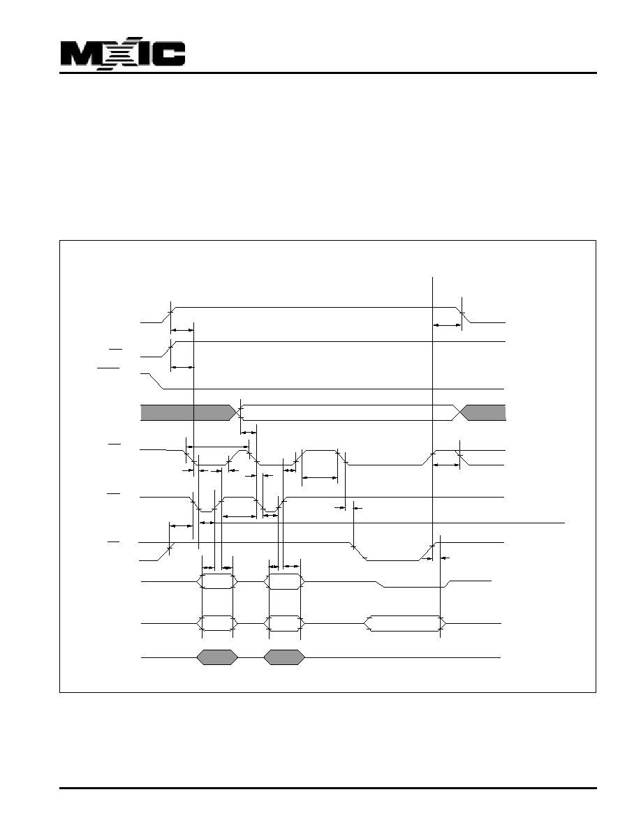
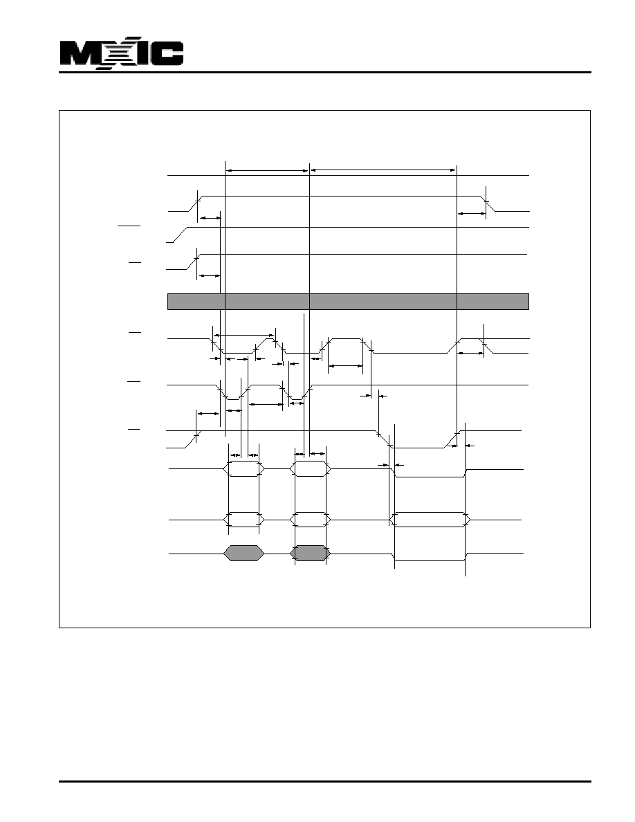
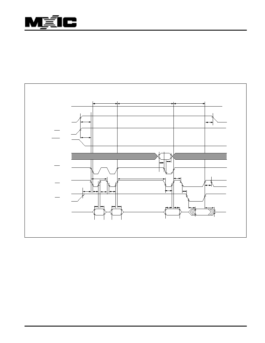
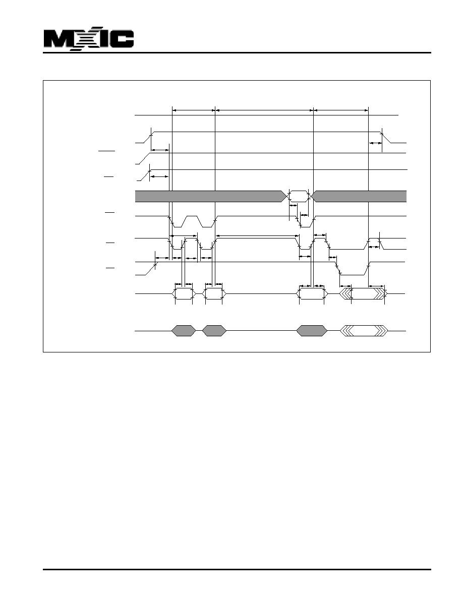
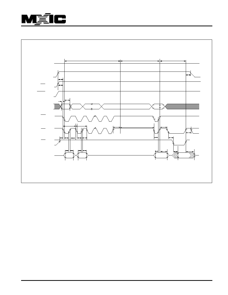
AUTOMATIC PROGRAMMING TIMING WAVEFORM
One byte data is programmed. Verify in fast algorithm
and additional programming by external control are not
required because these operations are excuted auto-
matically by internal control circuit. Programming
completion can be verified by status register after
automatic Program starts.
AUTOMATIC PROGRAMMING TIMING WAVEFORM-BYTE MODE
tCWC
tAS
tCEP
tOES
tCEP
tCES
tDS
tDH
tDH
tDS
tDF
Vcc 5V
CE
OE
12V
Vpp
0V
tVPH
DATA
Q0~Q2
WE
ADD
A-1~16
tCEPH1
tVPS
DIN
Valid SRD
tCS
tCS
tCH
tCH
ADD Valid
tCESC
VIH
VIL
BYTE
DATA
Q3~Q7
DATA
Q8~Q14
VIH
VIL
VIH
VIL
VIH
VIL
VIH
VIL
VIH
VIL
VIH
VIL
VIH
VIL
DIN
Command In
High Z
tCESP
10H/or 40H
RP
tPHEL
Command In
21
MX28F2100B
P/N: PM0382
REV. 1.5, MAR. 24, 1998
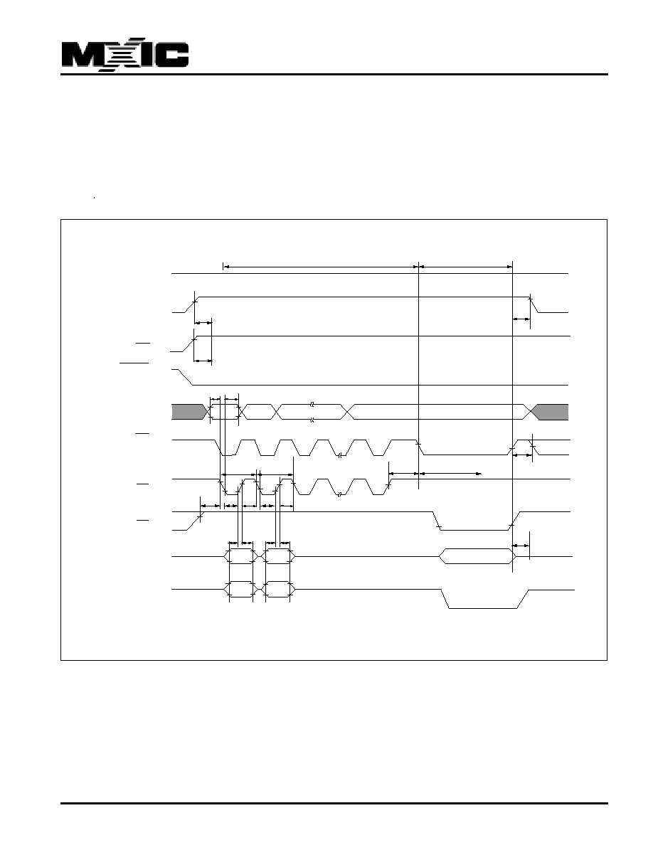
AUTOMATIC PROGRAMMING TIMING WAVEFORM-WORD MODE
DIN
tCWC
tAS
tCEP
tOES
tCEP
tCES
tDS
tDH
tDH
tDS
tDF
Vcc 5V
CE
OE
12V
Vpp
0V
tVPH
DATA
Q0~Q2
Setup Auto Program/
Program command
Vaild SRD
WE
ADD
A0~16
tCEPH1
tAH1
tDPA
tVPS
DIN
DIN
tCS
tCS
tCH
tCH
ADD Valid
tCESC
VIH
VIL
BYTE
DATA
Q3~Q7
DATA
Q8~Q15
VIH
VIL
VIH
VIL
VIH
VIL
VIH
VIL
VIH
VIL
VIH
VIL
VIH
VIL
tCESP
Command In
10H/or 40H
tVPS
RP
Command In
22
MX28F2100B
P/N: PM0382
REV. 1.5, MAR. 24, 1998
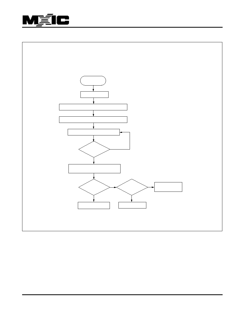
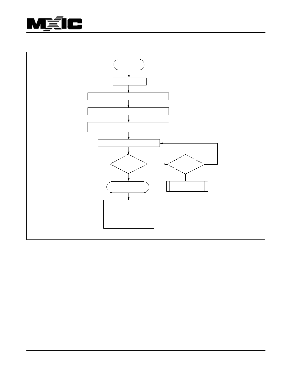
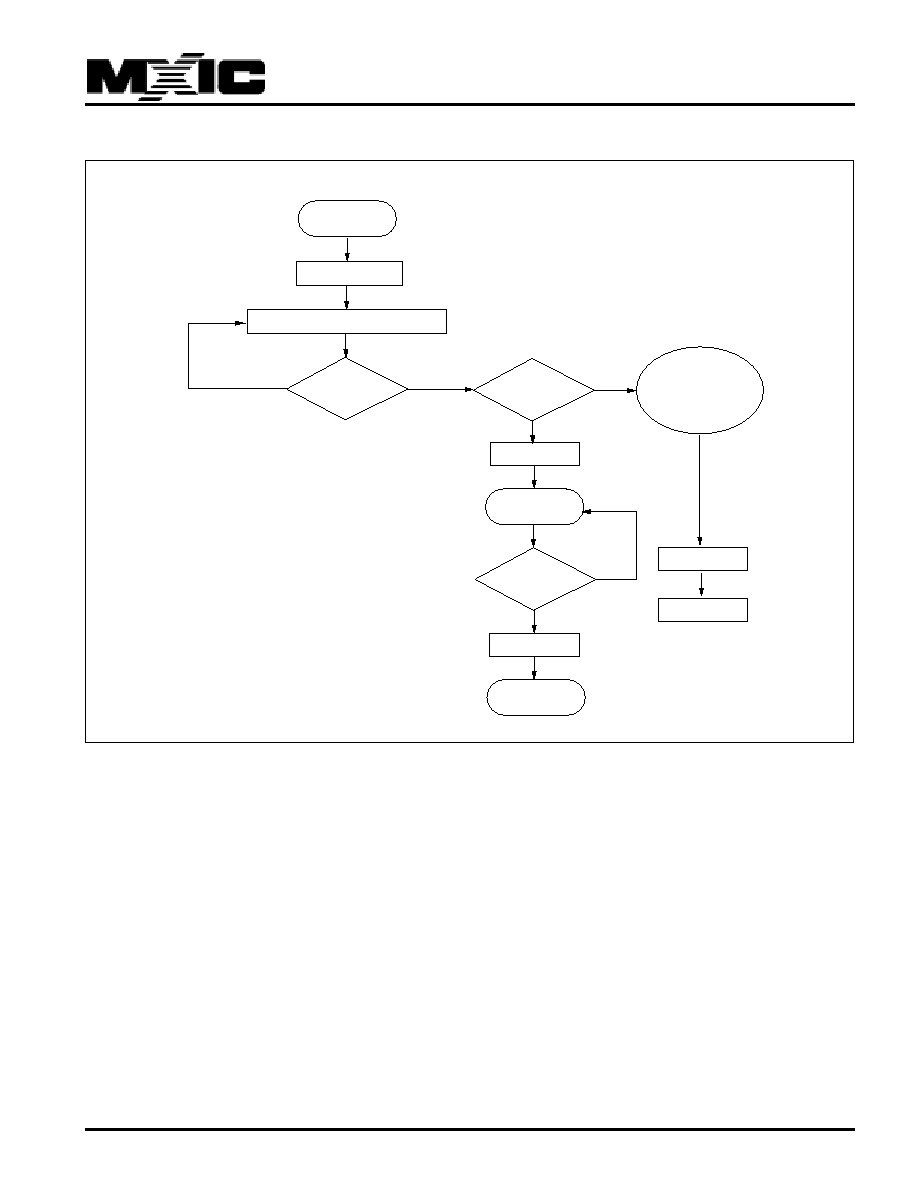
Program Command Sequence
(Address/Command)
AUTOMATIC PROGRAMMING ALGORITHM FLOWCHART
START
Apply VppH
Write Set up Auto Program Command (10H/40H)
Read Status Register
Write Auto Program Command(A/D)
Status Register Ready
Full Status Check
Vpp Range Error
YES
1
NO
SR.7=1
SR.3=
SR.4=
0
0
1
Program Error
Programming
Successfully
23
MX28F2100B
P/N: PM0382
REV. 1.5, MAR. 24, 1998
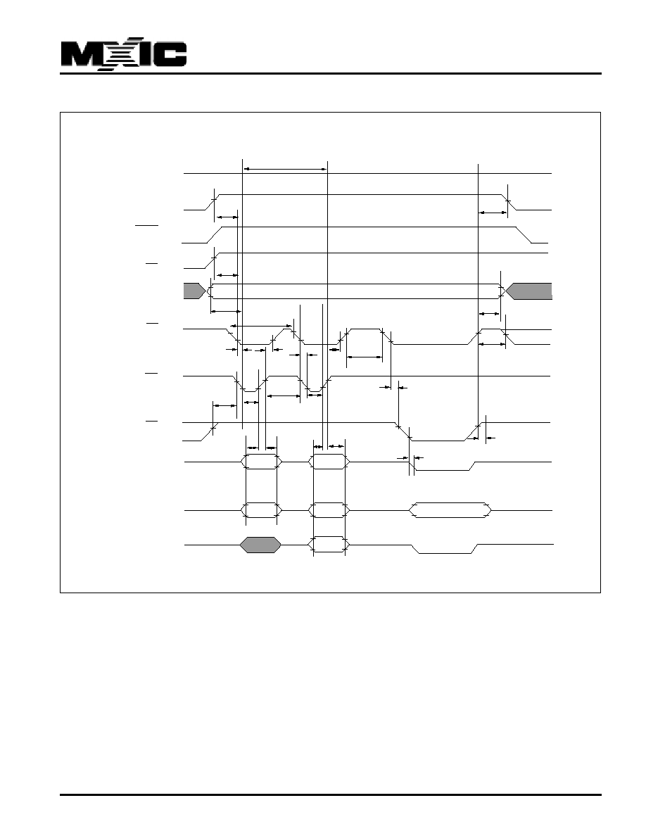
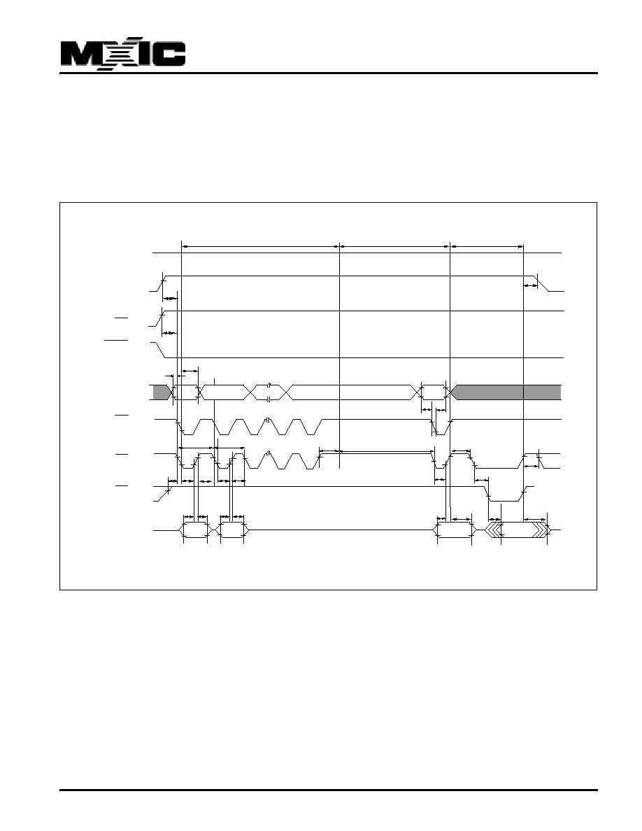
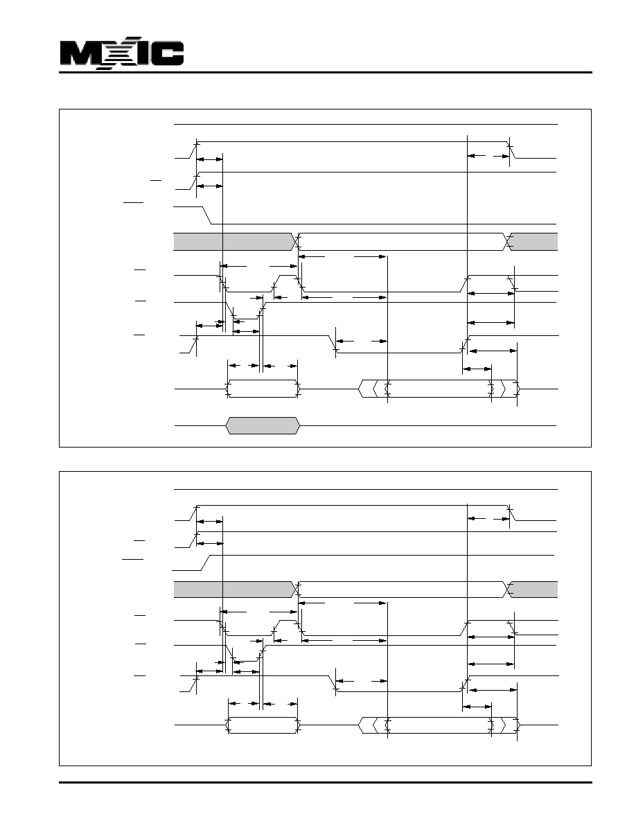
AUTOMATIC CHIP ERASE TIMING WAVEFORM
All data in chip are erased. External erase verify is not
required because data is erased automatically by internal
control circuit. Erasure completion can be verified by
Status register contents after automatic erase starts.
AUTOMATIC CHIP ERASE TIMING WAVEFORM-BYTE MODE
tCWC
tCEP
tOES
tCEP
tCES
tDS
tDH
tDH
tDS
tDF
Vcc 5V
CE
OE
12V
Vpp
0V
tVPH
DATA
Q0~Q2
Auto Erase
Setup Auto Chip Erase/
Erase command
WE
ADD
A-1~16
tCEPH1
tDPA
tVPS
Vaild SRD
tCS
tCS
tCH
tCH
tCESP
tCESC
VIH
VIL
BYTE
DATA
Q3~Q7
DATA
Q8~Q14
tAETC
Command In
NOTE:
Erase Suspend and Read Array modes are not included in this waveform.
VIH
VIL
VIH
VIL
VIH
VIL
VIH
VIL
VIH
VIL
VIH
VIL
VIH
VIL
30H
30H
High Z
Command In
Command In
Command In
RP
tPHEL
24
MX28F2100B
P/N: PM0382
REV. 1.5, MAR. 24, 1998
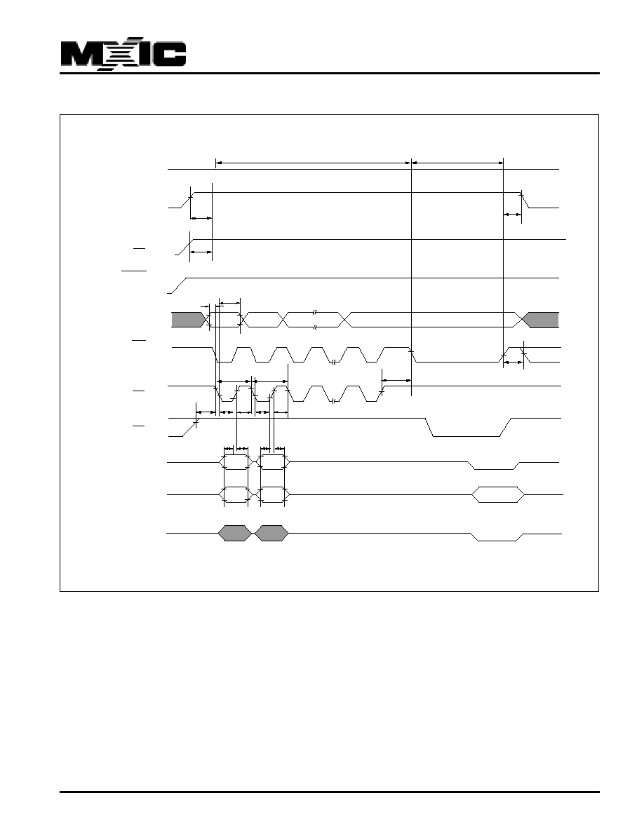
AUTOMATIC CHIP ERASE TIMING WAVEFORM-WORD MODE
tCWC
tCEP
tOES
tCEP
tCES
tDS
tDH
tDH
tDS
tDF
Vcc 5V
CE
OE
12V
Vpp
0V
tVPH
DATA
Q0~Q3
Auto Erase
Setup Auto Chip Erase/
Erase command
WE
ADD
A0~16
tCEPH1
tDPA
tVPS
Valid SRD
tCS
tCS
tCH
tCH
tCESP
tCESC
VIH
VIL
BYTE
DATA
Q7
DATA
Q8~Q15
Command In
NOTE:
Erase Suspend and Read Array modes are not included in this waveform.
VIH
VIL
VIH
VIL
VIH
VIL
VIH
VIL
VIH
VIL
VIH
VIL
VIH
VIL
30H
30H
Command In
Command In
Command In
RP
tPHEL

25
MX28F2100B
P/N: PM0382
REV. 1.5, MAR. 24, 1998
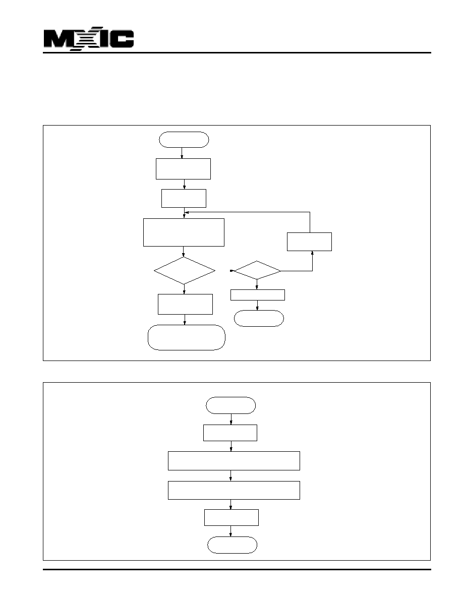
AUTOMATIC CHIP ERASE ALGORITHM FLOWCHART
START
Apply VppH
Write Set up Auto Chip Erase Command (30H)
0
Read Status Register
Write Auto Chip Erase Command(30H)
SR.7=
Operation Done.
Device Stays at
Read Status Register Mode
To Check SR3, 4, 5
To See Whether Erase Successfully
1
Chip Erase completed
To Execute
Suspend Mode
NO
YES
Erase Suspend/
Erase Resume Flow
26
MX28F2100B
P/N: PM0382
REV. 1.5, MAR. 24, 1998
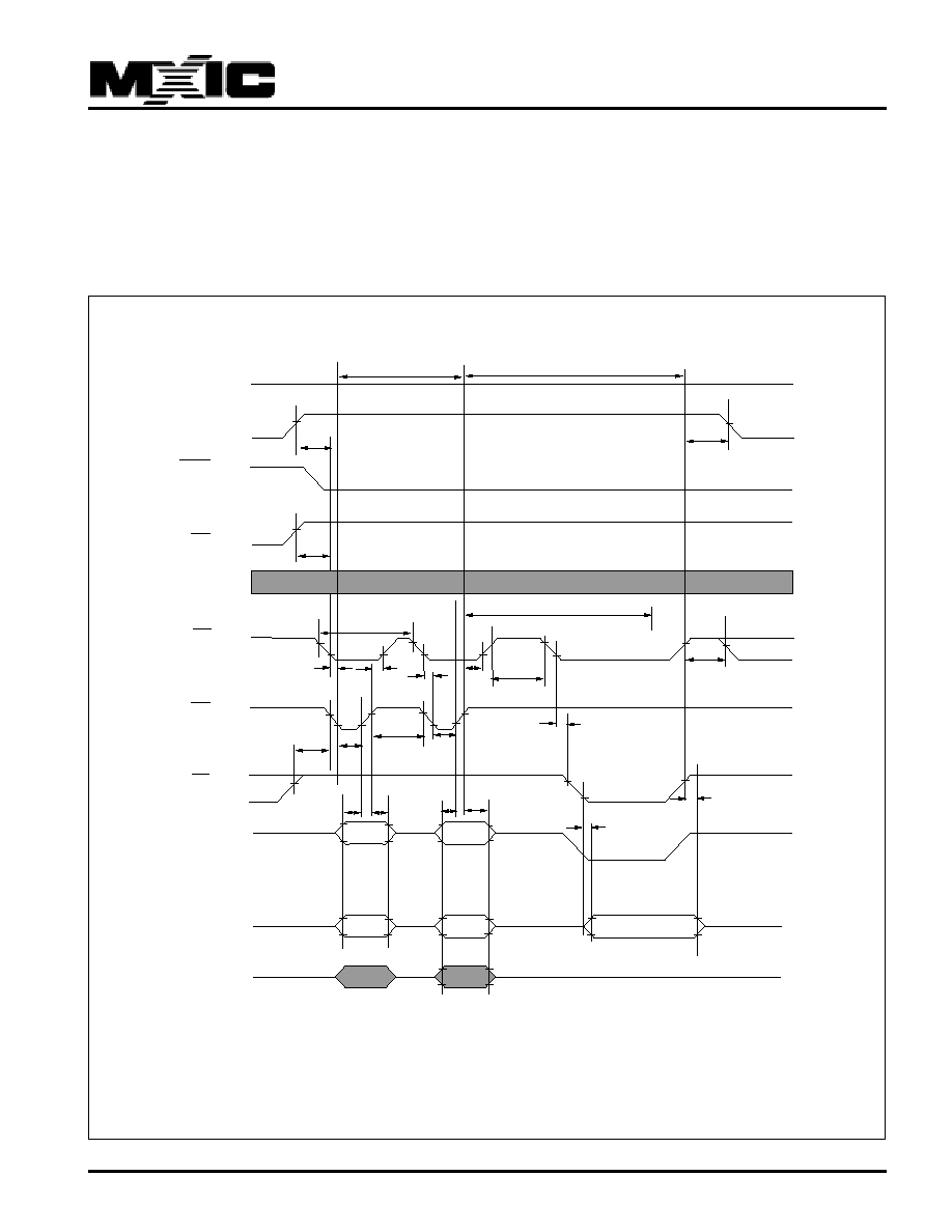
AUTOMATIC BLOCK ERASE TIMING WAVEFORM
Block data (refer to page 1 for block structure) are erased.
External erase verify is not required because data are
erased automatically by internal control circuit. Erasure
completion can be verified by status register contents
after automatic erase starts.
AUTOMATIC BLOCK ERASE TIMING WAVEFORM-BYTE MODE
Vcc 5V
tCEP
tOES
tDF
Command in
OE
Command in
Command in
Command in
tCESC
tDS
tDH
tDS
tDH
Block
address 0
Block
address 1
tCWC
tBALC
tCEP
12V
Vpp
0V
Block
address #
Command #20H Command #D0H
tVPH
tBAL
tAETB
Q3~Q7
Q0~Q2
Auto block erase & Status register read
A-1~ A16
CE
WE
tCEPH2
tCEPH1
Setup auto block erase/erase command
tVPS
tAH
tAS
PBYTE
VIH
VIL
VIH
VIL
VIH
VIL
VIH
VIL
VIH
VIL
VIH
VIL
VIH
VIL
RP
tPHEL
Valid Data
27
MX28F2100B
P/N: PM0382
REV. 1.5, MAR. 24, 1998
AUTOMATIC BLOCK ERASE TIMING WAVEFORM-WORD MODE
Vcc 5V
tCEP
tOES
Command in
OE
Command in
Command in
Command in
tCESC
tDS
tDH
tDS
tDH
Block
address 0
Block
address 1
tCWC
tBALC
tCEP
12V
Vpp
0V
Block
address #
Command #20H Command #D0H
tVPH
tVPS
tBAL
Q0~Q2
Auto Block Erase
A0 ~ A16
CE
WE
tCEPH2
tCEPH1
Setup Auto Block Erase/Erase command
tAH
tAS
BYTE
VIH
VIL
VIH
VIL
VIH
VIL
VIH
VIL
VIH
VIL
VIH
VIL
VIH
VIL
Valid SRD
Q3~Q7
VIH
VIL
RP
tPHEL
Q8~Q15
28
MX28F2100B
P/N: PM0382
REV. 1.5, MAR. 24, 1998
AUTOMATIC BLOCK ERASE ALGORITHM FLOWCHART
START
Apply VppH
Write Set up auto chip Erase Command (20H)
0
Read Status Register
Write Auto chip Erase Command(D0H)
SR.7=
Operation Done.
Device Stays at
Read Status Register Mode
To Check SR3, 4, 5
To See Whether Erase Successfully.
1
Chip Erase completed
To Execute
Suspend Mode
NO
YES
Erase Suspend/
Erase Resume Flow
Load Other Sectors Address If Necessary
(Load Other Sector Address)
29
MX28F2100B
P/N: PM0382
REV. 1.5, MAR. 24, 1998
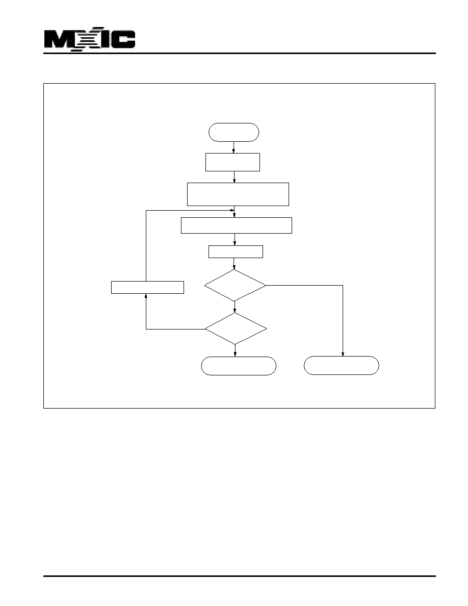
ERASE SUSPEND/ERASE RESUME FLOWCHART
START
Write Data B0H
1
Read Status Register
SR.7=
0
SR.6=
0
1
YES
NO
Erase Completed
Check SR3, 4, 5
To See Whether
Erase Successfully
Write Data FFH
Write Data D0H
Continue Erase
Reading End
Read Array
Write FFH
Read Array
30
MX28F2100B
P/N: PM0382
REV. 1.5, MAR. 24, 1998
FAST HIGH-RELIABILITY CHIP ERASE
This device can be applied the Fast High-Reliability Chip
erase algorithm shown in the following flowchart.
CHIP ERASE FLOW
FAST HIGH-RELIABILITY CHIP ERASE FLOWCHART
Command Sequence
START
ALL BITS
END
NO
YES
FAIL
ALL BITS VERIFIED
PGM "0"
N = 0
CHIP ERASE FLOW
ERSVFY FLOW
N = 1024?
CHIP ERASE FAIL
APPLY
VPP = VCC
CHIP ERASE
COMPLETE
N = N+1
START
Apply
WRITE SETUP CHIP ERASE COMMAND
END
VPP = VPPH
( 20H )
WRITE CHIP ERASE COMMAND
( 20H )
WAIT
10 ms
31
MX28F2100B
P/N: PM0382
REV. 1.5, MAR. 24, 1998
ERASE VERIFY FLOW
START
WRITE ERASE VERIFY COMMAND
WAIT 6 us
LAST ADDRESS ?
INCREMENT ADDRESS
NO
YES
NO
YES
APPLY
VPP = VPPH
ADDRESS =
FIRST ADDRESS OF ERASED BLOCKS
OR LAST VERIFY FAILED ADDRESS
( A0H )
ERSVFY
FFH ?
ERASE VERIFY
COMPLETE
GO TO ERASE FLOW
AGAIN OR ABORT
32
MX28F2100B
P/N: PM0382
REV. 1.5, MAR. 24, 1998
FAST HIGH-RELIABILITY CHIP ERASE TIMING WAVEFORM
All data in chip are erased. Control verification and
additional erasure externally according to fast high-relia-
bility chip erase flowchart. Successful erasure comple-
tion can be verified by status registers.
FAST HIGH-RELIABILITY CHIP ERASE TIMING WAVEFORM-BYTE MODE
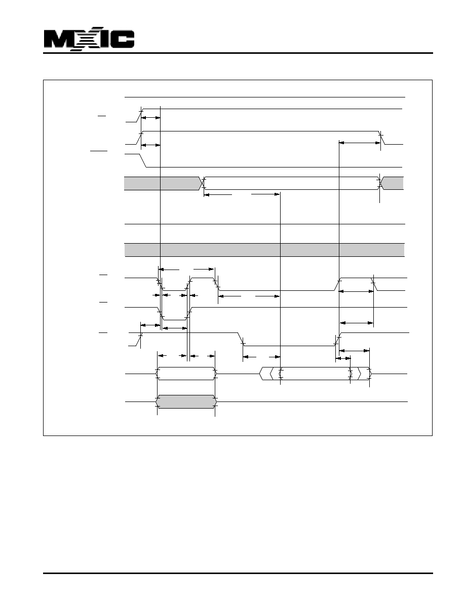
Vcc 5V
tCEP
tOES
tDF
Command in
CE
OE
tCESC
tCEP
tDS
tDH
tDS
tDH
tCWC
tET
tCEP
tCES
tVA
Command in
tDS
12V
Vpp
0V
Command #20H Command #20H
Command #A0H
tVPH
tPHEL
Q0~Q7
Erase Verify
Chip Erase
tAS
tAH
Verify
Address
tCESV
Command in
tDH
Valid Data
A-1 ~ A16
WE
tCEPH1
Setup Chip Erase/
Erase command
BYTE
VIH
VIL
VIH
VIL
VIH
VIL
VIH
VIL
VIH
VIL
VIH
VIL
RP
tVPS
33
MX28F2100B
P/N: PM0382
REV. 1.5, MAR. 24, 1998
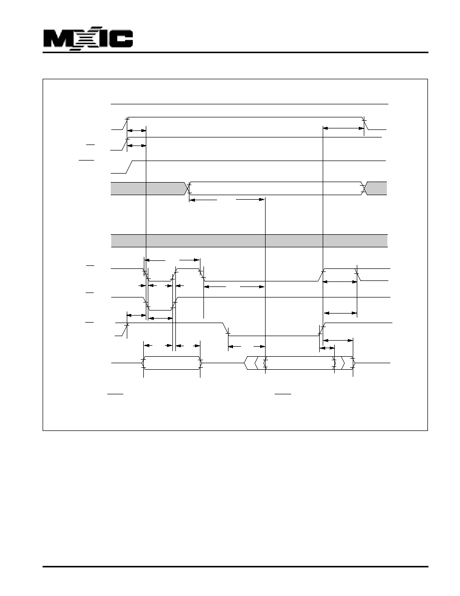
FAST HIGH-RELIABILITY CHIP ERASE TIMING WAVEFORM-WORD MODE
Vcc 5V
tCEP
tOES
tDF
Command in
CE
OE
tCESC
tCEP
tDS
tDH
tDS
tDH
tCWC
tET
tCEP
tCES
tVA
Command in
tDS
12V
Vpp
0V
Command #20H Command #20H
Command #A0H
tVPH
tVPS
Q0~Q7
Erase Verify
Chip erase
tAS
tAH
Verify
Address
tCESV
Command in
tDH
A0 ~ A16
WE
tCEPH1
Setup chip erase/
erase command
Valid Data
BYTE
VIH
VIL
VIH
VIL
VIH
VIL
VIH
VIL
VIH
VIL
VIH
VIL
Q8~Q15
VIH
VIL
RP
tPHEL
Valid Data
34
MX28F2100B
P/N: PM0382
REV. 1.5, MAR. 24, 1998
FAST HIGH-RELIABILITY BLOCK ERASE
This device can be applied to the fast high-reliability block
erase algorithm shown in the following flowchart.
BLOCK ERASE FLOW
FAST HIGH-RELIABILITY BLOCK ERASE FLOWCHART
Command Sequence
START
Apply
WRITE SETUP BLOCK ERASE COMMAND
END
VPP = VPPH
WRITE BLOCK ERASE COMMAND
( 60H )
WAIT
10 ms
( LOAD FIRST SECTOR ADDRESS , 60H )
LOAD OTHER SECTORS' ADDRESS
IF NECESSARY
( LOAD OTHER SECTOR ADDRESS )
START
END
NO
YES
FAIL
ALL BITS VERIFIED
N = 0
BLOCK ERASE FLOW
ERSVFY FLOW
N = 1024?
BLOCK ERASE FAIL
APPLY
VPP = VCC
BLOCK ERASE
COMPLETE
N = N+1
For selected block(s),
All bits PGM"0"
35
MX28F2100B
P/N: PM0382
REV. 1.5, MAR. 24, 1998
ERASE VERIFY FLOW
START
WRITE ERASE VERIFY COMMAND
WAIT 6 us
LAST ADDRESS ?
INCREMENT ADDRESS
NO
YES
NO
YES
APPLY
VPP = VPPH
ADDRESS =
FIRST ADDRESS OF ERASED BLOCKS
OR LAST VERIFY FAILED ADDRESS
( A0H )
ERSVFY
FFH ?
ERASE VERIFY
COMPLETE
GO TO ERASE FLOW
AGAIN OR ABORT
36
MX28F2100B
P/N: PM0382
REV. 1.5, MAR. 24, 1998
FAST HIGH-RELIABILITY BLOCK ERASE TIMING WAVEFORM
Indicated block data are erased. Control verification and
additional erasure externally according to fast high-reli-
ability block erase flowchart.
FAST HIGH-RELIABILITY BLOCK ERASE TIMING WAVEFORM-BYTE MODE
Vcc 5V
tDS
tDF
Command in
tDS
tDH
tDS
tDH
tVA
Command in
Command in
tDH
tBAL
tET
tCEP
tAS tAH
tCESC
tOES tCEP
tCEP
tCWC
tBALC
Block
address 0
Block
address 1
tAS
CE
OE
12V
Vpp
0V
Command #60H Command #60H
Command #A0H
tVPH
Q0~Q7
Erase Verify
Block Erase
tCESV
tCES
Valid Data
Verify
address
A-1 ~ A16
WE
Block
address #
tCEPH1
tCEPH2
Setup Block Erase/Erase Command
tVPS
tAH
VIH
VIL
VIH
VIL
VIH
VIL
VIH
VIL
VIH
VIL
VIH
VIL
BYTE
RP
tPHEL
37
MX28F2100B
P/N: PM0382
REV. 1.5, MAR. 24, 1998
FAST HIGH-RELIABILITY BLOCK ERASE TIMING WAVEFORM-WORD MODE
Vcc 5V
tDS
tDF
Command in
tDS
tDH
tDS
tDH
tVA
Command in
Command in
tDH
tBAL
tET
tCEP
tCESC
tOES tCEP
tCEP
tCWC
tBALC
Block
address 0
Block
address 1
tAS
CE
OE
12V
Vpp
0V
Command #60H Command #60H
Command #A0H
tVPH
tVPS
Q0~Q7
Erase Verify
Block Erase
tCESV
tCES
Valid Data
Verify
address
A0 ~ A16
WE
Block
address #
tCEPH1
tCEPH2
Setup Block Erase/Erase Command
tAH
VIH
VIL
VIH
VIL
VIH
VIL
VIH
VIL
VIH
VIL
VIH
VIL
BYTE
RP
tPHEL
38
MX28F2100B
P/N: PM0382
REV. 1.5, MAR. 24, 1998
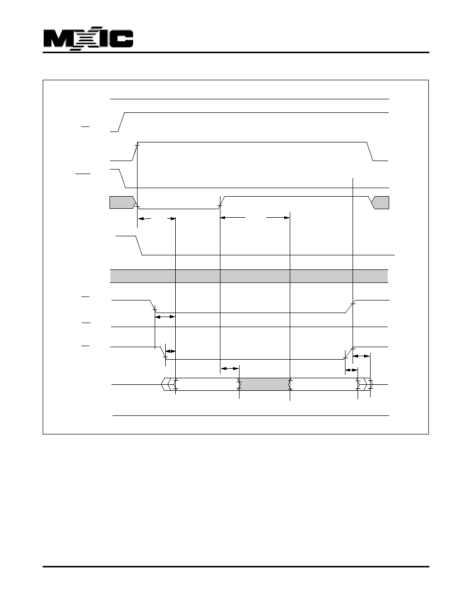
VPP HIGH READ TIMING WAVEFORM-BYTE MODE
VPP HIGH READ TIMING WAVEFORM-WORD MODE
tVPS
Address Valid
tACC
tVPH
tCESC
tCWC
tOES
tCEP
tCE
tOES
tDF
tOH
tDS
tDH
tOE
DATA valid
Vcc 5V
12V
Vpp
0V
ADD
A-1 ~16
CE
OE
DATA
Q0-7
FFH
WE
tCS
tCH
HIGH-Z
VIH
VIL
VIH
VIL
VIH
VIL
VIH
VIL
VIH
VIL
VIH
VIL
VIH
VIL
DATA
Q8-Q14
BYTE
Command in
RP
tPHEL
tVPS
Address Valid
tACC
tVPH
tCESC
tCWC
tOES
tCEP
tCE
tOES
tDF
tOH
tDS
tDH
tOE
DATA valid
Vcc 5V
12V
Vpp
0V
ADD
A0 ~16
CE
OE
DATA
Q0-15
Command in
WE
tCS
tCH
VIH
VIL
VIH
VIL
VIH
VIL
VIH
VIL
VIH
VIL
VIH
VIL
BYTE
XX FFH
RP
tPHEL
39
MX28F2100B
P/N: PM0382
REV. 1.5, MAR. 24, 1998
VPP LOW ID CODE READ TIMING WAVEFORM-BYTE MODE
tACC
tCE
tACC
tOE
tOH
tOH
tDF
DATA OUT
C2H
2BH
VID
VIH
VIL
ADD
A9
ADD
A1-A16
CE
OE
WE
ADD
A0
BYTE
DATA OUT
DATA
Q8-Q14
DATA
Q0-Q7
VCC
5V
VIH
VIL
VIH
VIL
VIH
VIL
VIH
VIL
VIH
VIL
VIH
VIL
VIH
VIL
HIGH-Z
VIH
VIL
ADD
A-1
RP
40
MX28F2100B
P/N: PM0382
REV. 1.5, MAR. 24, 1998
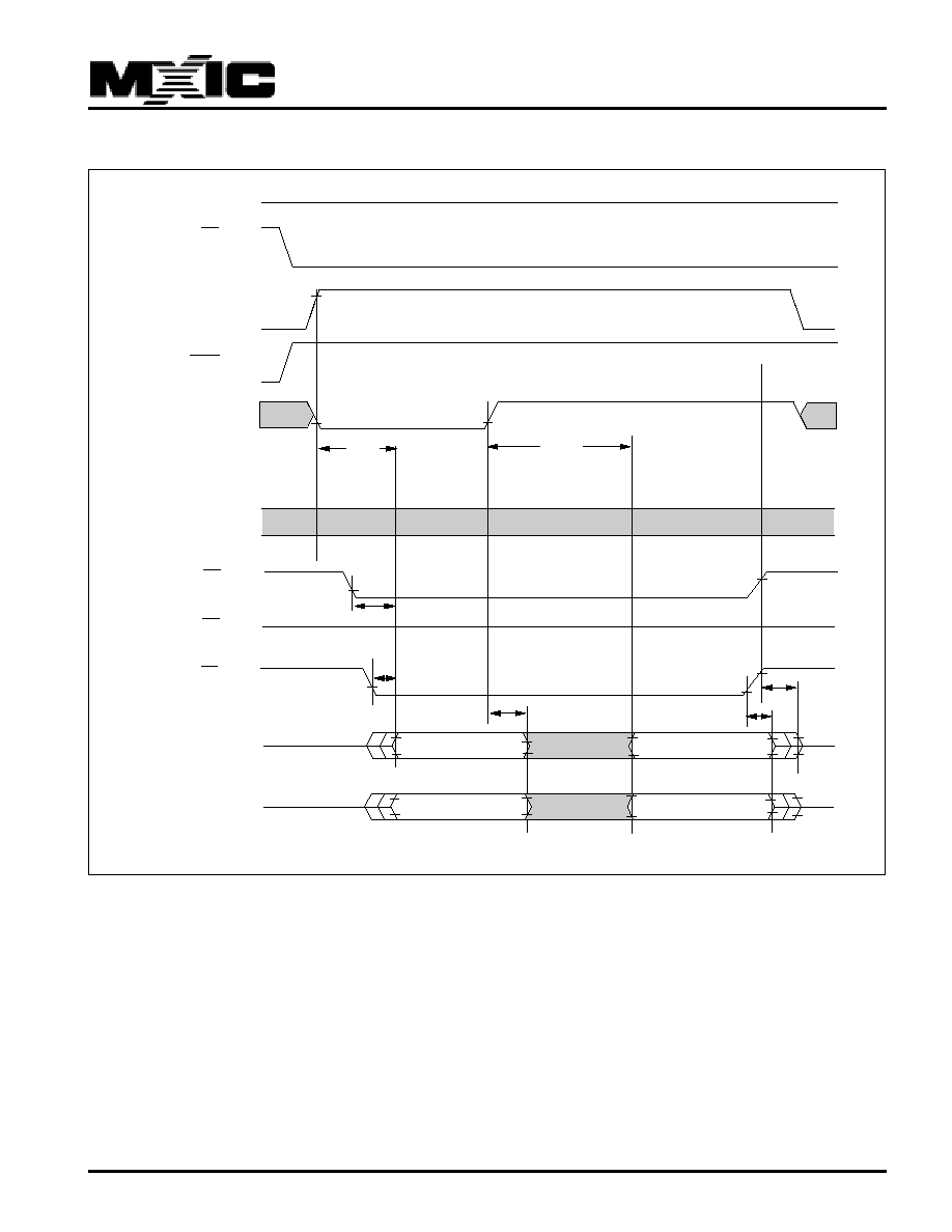
VPP LOW ID CODE READ TIMING WAVEFORM-WORD MODE
tACC
tCE
tACC
tOE
tOH
tOH
tDF
DATA OUT
00C2H
002BH
VID
VIH
VIL
ADD
A9
ADD
A1-A16
RP
OE
WE
ADD
A0
BYTE
DATA OUT
DATA OUT
DATA OUT
DATA
Q8-Q15
DATA
Q0-Q7
VCC
5V
VIH
VIL
VIH
VIL
VIH
VIL
VIH
VIL
VIH
VIL
VIH
VIL
VIH
VIL
VIH
VIL
CE
41
MX28F2100B
P/N: PM0382
REV. 1.5, MAR. 24, 1998
VPP HIGH ID CODE READ TIMING WAVEFORM-BYTE MODE
tCWC
tVPS
Address Valid 0 or 1
tACC
tVPH
tCESC
tOES
tCEP
tCE
tOES
tDF
tOH
tDS
tDH
tOE
DATA OUT
Vcc 5V
12V
Vpp
0V
CE
OE
DATA
Q0-Q7
Command in
C2H or 2BH
ADD
A1-A16
WE
tCS
tCH
DATA
Q8-Q14
ADD
A-1
ADD
A0
BYTE
HIGH-Z
VIH
VIL
VIH
VIL
VIH
VIL
VIH
VIL
VIH
VIL
VIH
VIL
VIH
VIL
VIH
VIL
VIH
VIL
90H
RP
tPHEL
42
MX28F2100B
P/N: PM0382
REV. 1.5, MAR. 24, 1998
VPP HIGH ID CODE READ TIMING WAVEFORM-WORD MODE
tCWC
tVPS
Address Valid 0 or 1
tACC
tVPH
tCESC
tOES
tCEP
tCE
tOES
tDF
tOH
tDS
tDH
tOE
DATA OUT
Vcc 5V
12V
Vpp
0V
CE
OE
DATA
Q0-Q15
Command in
00C2H or 002BH
ADD
A1-A16
WE
tCS
tCH
ADD
A0
BYTE
VIH
VIL
VIH
VIL
VIH
VIL
VIH
VIL
VIH
VIL
VIH
VIL
VIH
VIL
NOTE:
BYTE pin is treated as Address pin All timing specifications for BYTE pin are the same as those for address pin.
XX90H
RP
tPHEL

43
MX28F2100B
P/N: PM0382
REV. 1.5, MAR. 24, 1998
ORDERING INFORMATION
PLASTIC PACKAGE
PART NO.
ACCESS TIME
OPERATING CURRENT
STANDBY CURRENT
PACKAGE
(ns)
MAX.(mA)
MAX.(uA)
MX28F2100BMC-70 70
50
100
44 Pin SOP
MX28F2100BMC-90 90
50
100
44 Pin SOP
MX28F2100BMC-12 120
50
100
44 Pin SOP
MX28F2100BTC-70 70
50
100
48 Pin TSOP
(Normal Type)
MX28F2100BTC-90 90
50
100
48 Pin TSOP
(Normal Type)
MX28F2100BTC-12 120
50
100
48 Pin TSOP
(Normal Type)
Revision History
Rev. #
Description
Date
1.4
Statement cleared for customer's better understanding
10/22/1997
44
MX28F2100B
P/N: PM0382
REV. 1.5, MAR. 24, 1998
PACKAGE INFORMATION
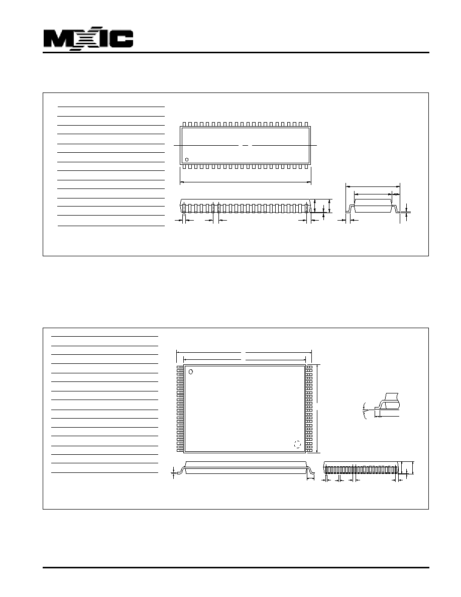
44-PIN PLASTIC SOP(500 mil)
ITEM MILLIMETERS INCHES
A
28.70 max.
1.130max.
B
1.10 [REF]
.043 [REF]
C
1.27 [TP]
.050 [TP]
D
.40
±
.10[Typ.]
.016
±
.004[Typ.]
E
.010 min.
.004 min.
F
3.00 max.
.118 max.
G
2.80
±
.13
.110
±
.005
H
16.04
±
.30
.631
±
.012
I
12.60
.496
J
1.72
.068
K
.15
±
.10 [Typ.] .006
±
.004[Typ.]
L
.80
±
.20
.031
±
.008
NOTE: Each lead certerline is located within
.25mm[.01 inch] of its true position [TP] at a
maximum at maximum material condition.
ITEM
MILLIMETERS
INCHES
A
20.0
±
.20
.787
±
.008
B
18.40
±
.10
.724
±
.004
C
12.20 max.
.480 max.
D
0.15 [Typ.]
.006 [Typ.]
E
.80 [Typ.]
.031 [Typ.]
F
.20
±
.10
.008
±
.004
G
.30
±
.10
.012
±
.004
H
.50 [Typ.]
.020 [Typ.]
I
.45 max.
.018 max.
J
0 ~ .20
0 ~ .008
K
1.00
±
.10
.039
±
.004
L
1.27 max.
.050 max.
M
.50
.020
N
0 ~5∞
.500
NOTE: Each lead certerline is located within
.25mm[.01 inch] of its true position [TP] at a
maximum at maximum material condition.
48-PIN PLASTIC TSOP
A
B
C
D
E
F
G
H
I
J
K
L
M
N
1
22
23
44
A
D
C
B
E
G
F
H
I
J
K
L

45
MX28F2100B
M
ACRONIX
I
NTERNATIONAL
C
O.,
L
TD.
HEADQUARTERS:
TEL:+886-3-578-8888
FAX:+886-3-578-8887
EUROPE OFFICE:
TEL:+32-2-456-8020
FAX:+32-2-456-8021
JAPAN OFFICE:
TEL:+81-44-246-9100
FAX:+81-44-246-9105
SINGAPORE OFFICE:
TEL:+65-747-2309
FAX:+65-748-4090
TAIPEI OFFICE:
TEL:+886-3-509-3300
FAX:+886-3-509-2200
M
ACRONIX
A
MERICA,
I
NC.
TEL:+1-408-453-8088
FAX:+1-408-453-8488
CHICAGO OFFICE:
TEL:+1-847-963-1900
FAX:+1-847-963-1909
http : //www.macronix.com
MACRONIX INTERNATIONAL CO., LTD. reserves the rignt to change product and specifications without notice.