1
P/N:PM0556
REV. 1.3, NOV. 11, 2002
MX29F022/022NT/B
2M-BIT[256K x 8]CMOS FLASH MEMORY
FEATURES
∑
262,144x 8 only
∑
Fast access time: 55/70/90/120ns
∑
Low power consumption
- 30mA maximum active current
- 1uA typical standby current@5MHz
∑
Programming and erasing voltage 5V
±
10%
∑
Command register architecture
- Byte Programming (7us typical)
- Sector Erase (16K-Byte x1, 8K-Byte x 2, 32K-Byte
x1, and 64K-Byte x 3)
∑
Auto Erase (chip & sector) and Auto Program
- Automatically erase any combination of sectors or
the whole chip with Erase Suspend capability.
- Automatically programs and verifies data at speci-
fied address
∑
Erase Suspend/Erase Resume
- Suspends an erase operation to read data from, or
program data to, a sector that is not being erased,
then resumes the erase operation.
∑
Status Reply
- Data polling & Toggle bit for detection of program
and erase cycle completion.
∑
Chip protect/unprotect for 5V only system or 5V/12V
system
∑
100,000 minimum erase/program cycles
∑
Latch-up protected to 100mA from -1 to VCC+1V
∑
Boot Code Sector Architecture
- T = Top Boot Sector
- B = Bottom Boot Sector
∑
Hardware RESET pin
- Resets internal state machine to read mode
∑
Low VCC write inhibit is equal to or less than 3.2V
∑
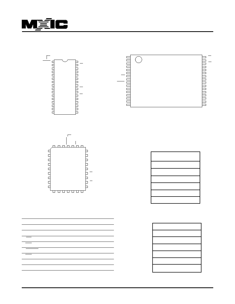
Package type:
- 32-pin PDIP
- 32-pin PLCC
- 32-pin TSOP (Type 1)
∑
20 years data retention
GENERAL DESCRIPTION
The MX29F022T/B is a 2-mega bit Flash memory
organized as 256K bytes of 8 bits only. MXIC's Flash
memories offer the most cost-effective and reliable read/
write non-volatile random access memor y. The
MX29F022T/B is packaged in 32-pin PDIP, PLCC and
32-pin TSOP(I). It is designed to be reprogrammed and
erased in-system or in-standard EPROM programmers.
The standard MX29F022T/B offers access time as fast
as 55ns, allowing operation of high-speed microproces-
sors without wait states. To eliminate bus contention,
the MX29F022T/B has separate chip enable (CE) and
output enable (OE) controls.
MXIC's Flash memories augment EPROM functionality
with in-circuit electrical erasure and programming. The
MX29F022T/B uses a command register to manage this
functionality. The command register allows for 100%
TTL level control inputs and fixed power supply levels
during erase and programming, while maintaining
maximum EPROM compatibility.
MXIC's Flash technology reliably stores memory
contents even after 100,000 erase and program cycles.
The MXIC cell is designed to optimize the erase and
programming mechanisms. In addition, the combina-
tion of advanced tunnel oxide processing and low
internal electric fields for erase and programming
operations produces reliable cycling. The MX29F022T/
B uses a 5.0V
±
10% VCC supply to perform the High
Reliability Erase and auto Program/Erase algorithms.
The highest degree of latch-up protection is achieved
with MXIC's proprietary non-epi process. Latch-up
protection is proved for stresses up to 100 milliamps on
address and data pin from -1V to VCC + 1V.

4
P/N:PM0556
REV. 1.3, NOV. 11, 2002
MX29F022/022NT/B
AUTOMATIC PROGRAMMING
The MX29F022T/B is byte programmable using the
Automatic Programming algorithm. The Automatic
Programming algorithm does not require the system to
time out or verify the data programmed. The typical chip
programming time of the MX29F022T/B at room tem-
perature is less than 2 seconds.
AUTOMATIC CHIP ERASE
The entire chip is bulk erased using 10ms erase pulses
according to MXIC's High Reliability Chip Erase
algorithm. Typical erasure at room temperature is
accomplished in less than two second. The device is
erased using the Automatic Erase algorithm. The
Automatic Erase algorithm automatically programs the
entire array prior to electrical erase. The timing and
verification of electrical erase are internally controlled
within the device.
AUTOMATIC SECTOR ERASE
The MX29F022T/B is sector(s) erasable using MXIC's
Auto Sector Erase algorithm. Sector erase modes allow
sectors of the array to be erased in one erase cycle. The
Automatic Sector Erase algorithm automatically pro-
grams the specified sector(s) prior to electrical erase.
The timing and verification of electrical erase are inter-
nally controlled by the device.
AUTOMATIC PROGRAMMING ALGORITHM
MXIC's Automatic Programming algorithm requires the
user to only write a program set-up commands (include
2 unlock write cycle and A0H) include 2 unlock write
cycle and A0H and a program command (program data
and address). The device automatically times the pro-
gramming pulse width, verifies the program verification,
and counts the number of sequences. A status bit simi-
lar to DATA polling and a status bit toggling between con-
secutive read cycles, provides feedback to the user as
to the status of the programming operation.
AUTOMATIC ERASE ALGORITHM
MXIC's Automatic Erase algorithm requires the user to
write commands to the command register using stan-
dard microprocessor write timings. The device will au-
tomatically pre-program and verify the entire array. Then
the device automatically times the erase pulse width,
verifies the erase, and counts the number of sequences.
A status bit similar to DATA polling and status bit tog-
gling between consecutive read cycles provides feed-
back to the user as to the status of the programming
operation.
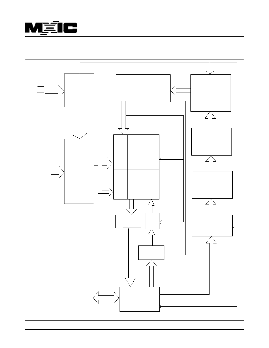
Commands are written to the command register using
standard microprocessor write timings. Register con-
tents serve as inputs to an internal state-machine which
controls the erase and programming circuitry. During
write cycles, the command register internally latches
address and data needed for the programming and erase
operations. During a system write cycle addresses are
latched on the falling edge, and data are latched on the
rising edge of WE .
MXIC's Flash technology combines years of EPROM
experience to produce the highest levels of quality, reli-
ability, and cost effectiveness. The MX29F022T/B elec-
trically erases all bits simultaneously using Fowler-
Nordheim tunneling. The bytes are programmed one
byte at a time using the EPROM programming mecha-
nism of hot electron injection.
During a program cycle, the state-machine will control
the program sequences and command register will not
respond to any command set. During a Sector Erase
cycle, the command register will only respond to Erase
Suspend command. After Erase Suspend is completed,
the device stays in read mode. After the state machine
has completed its task, it will allow the command regis-
ter to respond to its full command set.
5
P/N:PM0556
REV. 1.3, NOV. 11, 2002
MX29F022/022NT/B
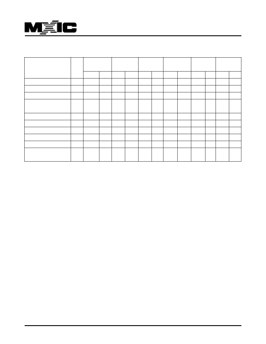
First Bus
Second Bus Third Bus
Fourth Bus
Fifth Bus
Sixth Bus
Command
Bus
Cycle
Cycle
Cycle
Cycle
Cycle
Cycle
Cycle
Addr
Data Addr
Data
Addr
Data Addr
Data Addr
Data Addr Data
Reset
1
XXXH F0H
Read
1
RA
RD
Read Silicon ID
4
555H
AAH 2AAH 55H
555H 90H
ADI
DDI
Chip Protect Verify
4
555H
AAH 2AAH 55H
555H 90H
(SA)
00H
X02H
01H
Program
4
555H
AAH 2AAH 55H
555H A0H
PA
PD
Chip Erase
6
555H
AAH 2AAH 55H
555H 80H
555H
AAH 2AAH 55H 555H 10H
Sector Erase
6
555H
AAH 2AAH 55H
555H 80H
555H
AAH 2AAH 55H SA
30H
Sector Erase Suspend
1
XXXH B0H
Sector Erase Resume
1
XXXH 30H
Unlock for chip
6
555H
AAH 2AAH 55H
555H 80H
555H
AAH 2AAH 55H 555H 20H
protect/unprotect
Note:
1. ADI = Address of Device identifier; A1=0,A0 =0 for manufacture code,A1=0, A0 =1 for device code (Refer to Table
3).
DDI = Data of Device identifier : C2H for manufacture code, 36H/37H for device code.
X = X can be VIL or VIH
RA=Address of memory location to be read.
RD=Data to be read at location RA.
2. PA = Address of memory location to be programmed.
PD = Data to be programmed at location PA.
SA = Address to the sector to be erased.
3. The system should generate the following address patterns: 555H or 2AAH to Address A0~A10.
Address bit A11~A17=X=Don't care for all address commands except for Program Address (PA) and Sector
Address (SA). Write Sequence may be initiated with A11~A17 in either state.
4. For Chip Protect Verify operation: If read out data is 01H, it means the chip has been protected. If read out data is
00H, it means the chip is still not being protected.
TABLE 1. SOFTWARE COMMAND DEFINITIONS