
FEATURES
∑ 5V
±
10% for read, erase and write operation
∑ 131072x8/ 65536x16 switchable
∑ Fast access time:55/70/90/120ns
∑ Low power consumption
- 40mA maximum active current(5MHz)
- 1
uA
typical standby current
∑ Command register architecture
- Byte/ Word Programming (7us/ 12us typical)
- Erase (16K-Bytex1, 8K-Bytex2, 32K-Bytex1, and
64K-Byte x1)
∑ Auto Erase (chip) and Auto Program
- Automatically erase any combination of sectors or
with Erase Suspend capability.
- Automatically program and verify data at specified
address
∑ Status Reply
- Data polling & Toggle bit for detection of program
and erase cycle completion.
∑ Compatibility with JEDEC standard
- Pinout and software compatible with single-power
supply Flash
- Superior inadvertent write protection
∑ Sector protection
- Hardware method to disable any combination of
sectors from program or erase operations
- Sector protect/unprotect for 5V only system or 5V/
12V system
∑ 100,000 minimum erase/program cycles
∑ Latch-up protected to 100mA from -1 to VCC+1V
∑ Boot Code Sector Architecture
- T = Top Boot Sector
- B = Bottom Boot Sector
∑ Low VCC write inhibit is equal to or less than 3.2V
∑ Package type:
- 44-pin SOP
- 48-pin TSOP
∑ Ready/Busy pin(RY/BY)
- Provides a hardware method or detecting program
or erase cycle completion
∑ Erase suspend/ Erase Resume
- Suspend an erase operation to read data from, or
program data to a sector that is not being erased,
then resume the erase operation.
∑ Hardware RESET pin
- Hardware method of resetting the device to reading
the device to reading array data.
∑ 20 years data retention
GENERAL DESCRIPTION
The MX29F100T/B is a 1-mega bit Flash memory
organized as 131,072 bytes or 65,536 words.
MXIC's Flash memories offer the most cost-effective
and reliable read/write non-volatile random access
memory. The MX29F100T/B is packaged in 44-pin
SOP and 48-pin TSOP. It is designed to be repro-
grammed and erased in-system or in-standard
EPROM programmers.
The standard MX29F100T/B offers access time as
fast as 55ns, allowing operation of high-speed micro-
processors without wait states. To eliminate bus
contention, the MX29F100T/B has separate chip
enable (CE) and output enable (OE) controls.
MXIC's Flash memories augment EPROM function-
a l i t y w i t h i n - c i r c u i t e l e c t r i c a l e r a s u r e a n d
programming. The MX29F100T/B uses a command
register to manage this functionality. The command
register allows for 100% TTL level control inputs and
f i x e d p o w e r s u p p l y l e v e l s d u r i n g e r a s e a n d
programming, while maintaining maximum EPROM
compatibility.
MXIC Flash technology reliably stores memory con-
tents even after 100,000 erase and program cycles.
The MXIC cell is designed to optimize the erase and
programming mechanisms. In addition, the combi-
nation of advanced tunnel oxide processing and low
internal electric fields for erase and programming
o p e r a t i o n s p r o d u c e s r e l i a b l e c y c l i n g . T h e
MX29F100T/B uses a 5.0V
±
10% VCC supply to
perform the High Reliability Erase and auto
Program/Erase algorithms.
The highest degree of latch-up protection is
achieved with MXIC's proprietary non-epi process.
Latch-up protection is proved for stresses up to 100
milliamps on address and data pin from -1V to VCC
+ 1V.
MX29F100T/B
1M-BIT [128Kx8/64Kx16] CMOS FLASH MEMORY
1
P/N:PM0548
REV. 1.2, NOV. 12, 2001
2
P/N:PM0548
MX29F100T/B
REV. 1.2, NOV. 12, 2001
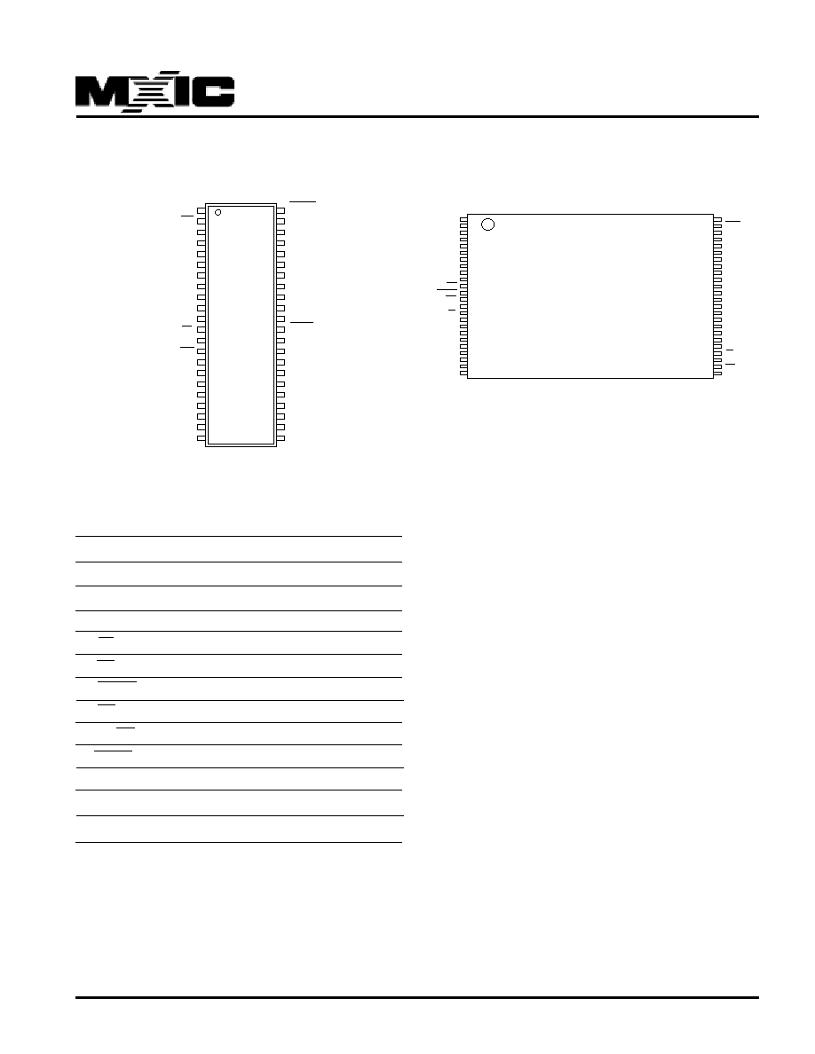
PIN CONFIGURATIONS
44SOP(500mil)
(NORMAL TYPE)
48 TSOP(TYPE I) (12mm x 20mm)
PIN DESCRIPTION:
SYMBOL
PIN NAME
A0-A15
Address Input
Q0-Q14
Data Input/Output
Q15/A-1
Q15(Word mode)/LSB addr.(Byte mode)
CE
Chip Enable Input
OE
Output Enable Input
RESET
Hardware Reset Pin, Active low
WE
Write Enable Input
RY/BY
Ready/Busy Output
BYTE
Word/Byte Selection Input
VCC
Power Supply Pin (+5V)
GND
Ground Pin
NC
Pin Not Connected Internally
2
3
4
5
6
7
8
9
10
11
12
13
14
15
16
17
18
19
20
21
22
44
43
42
41
40
39
38
37
36
35
34
33
32
31
30
29
28
27
26
25
24
23
NC
RY/BY
NC
A7
A6
A5
A4
A3
A2
A1
A0
CE
GND
OE
Q0
Q8
Q1
Q9
Q2
Q10
Q3
Q11
RESET
WE
A8
A9
A10
A11
A12
A13
A14
A15
NC
BYTE
GND
Q15/A-1
Q7
Q14
Q6
Q13
Q5
Q12
Q4
VCC
MX29F100T/B
A15
A14
A13
A12
A11
A10
A9
A8
NC
NC
WE
RESET
NC
NC
RY/BY
NC
NC
A7
A6
A5
A4
A3
A2
A1
1
2
3
4
5
6
7
8
9
10
11
12
13
14
15
16
17
18
19
20
21
22
23
24
NC
BYTE
GND
Q15/A-1
Q7
Q14
Q6
Q13
Q5
Q12
Q4
VCC
Q11
Q3
Q10
Q2
Q9
Q1
Q8
Q0
OE
GND
CE
A0
48
47
46
45
44
43
42
41
40
39
38
37
36
35
34
33
32
31
30
29
28
27
26
25
MX29F100T/B

5
P/N:PM0548
MX29F100T/B
REV. 1.2, NOV. 12, 2001
MXIC's Automatic Erase algorithm requires the user to
write commands to the command register using stand-
ard microprocessor write timings. The device will
automatically pre-program and verify the entire array.
Then the device automatically times the erase pulse
width, verifies the erase and counts the number of
sequences. A status bit toggling between consecutive
read cycles provides feedback to the user as to the
status of the programming operation.
Register contents serve as inputs to an internal state-
machine which controls the erase and programming
circuitry. During write cycles, the command register
internally latches address and data needed for the
programming and erase operations. During a system
write cycle, addresses are latched on the falling edge,
and data are latched on the rising edge of WE.
MXIC's Flash technology combines years of EPROM
experience to produce the highest levels of quality, relia-
bility, and cost effectiveness. The MX29F100T/B electri-
cally erases all bits simultaneously using Fowler-Nord-
heim tunneling. The bytes are programmed by using the
EPROM programming mechanism of hot electron
injection.
During a program cycle, the state-machine will control the
program sequences and command register will not re-
spond to any command set. During a Sector Erase cycle,
the command register will only respond to Erase Sus-
pend command. After Erase Suspend is complete, the
device stays in read mode. After the state machine has
completed its task, it will allow the command register to
respond to its full command set.
AUTOMATIC PROGRAMMING
The MX29F100T/B is byte/ word programmable using
the Automatic Programming algorithm. The Automatic
Programming algorithm does not require the system to
time out sequence or verify the data programmed. The
typical chip programming time of the MX29F100T/B at
room temperature is less than 3.5 seconds.
AUTOMATIC CHIP ERASE
The entire chip is bulk erased using 10 ms erase
pulses according to MXIC's Automatic Chip Erase
algorithm. Typical erasure at room temperature is
accomplished in less than 3 seconds. The Automatic
Erase algorithm automatically programs the entire
array prior to electrical erase. The timing and
verification of electrical erase are internally controlled
by the device.
AUTOMATIC SECTOR ERASE
The MX29F100T/B is sector(s) erasable using MXIC's
Auto Sector Erase algorithm. Sector erase modes allow
sectors of the array to be erased in one erase cycle. The
Automatic Sector Erase algorithm automatically pro-
grams the specified sector(s) prior to electrical erase.
The timing and verification of electrical erase are inter-
nally controlled by the device.
AUTOMATIC PROGRAMMING ALGORITHM
MXIC's Automatic Programming algorithm requires
the user to only write program set-up commands
(include 2 unlock write cycle and A0H) and a program
command (program data and address). The device
automatically times the programming pulse width,
verifies the program and counts the number of
sequences. A status bit similar to DATA polling and a
status bit toggling between consecutive read cycles,
provides feedback to the user as to the status of the
programming operation.
AUTOMATIC ERASE ALGORITHM

