 | –≠–ª–µ–∫—Ç—Ä–æ–Ω–Ω—ã–π –∫–æ–º–ø–æ–Ω–µ–Ω—Ç: MX29F1615 | –°–∫–∞—á–∞—Ç—å:  PDF PDF  ZIP ZIP |

GENERAL DESCRIPTION
The MX29F1615 is a 16-mega bit Flash memory organized
as either 1M wordx16 or 2M bytex8. MXIC's Flash
memories offer the most cost-effective and reliable read/
write non-volatile random access memory. The
MX29F1615 is packaged in 42-pin PDIP. It is designed
to be reprogrammed and in standard EPROM
programmers.
The standard MX29F1615 offers access times as fast as
90ns,allowing operation of high-speed microprocessors
without wait. To eliminate bus contention, the MX29F1615
has separate chip enables(CE) and output enable (OE)
control.
MXIC's Flash memories augment EPROM functionality
with electrical erasure and programming. The MX29F1615
uses a command register to manage this functionality.
The command register allows for 100% TTL level control
inputs and fixed power supply levels during erase and
programming, while maintaining maximum EPROM
compatibility.
1
FEATURES
∑
5V
±
10% write and erase
∑
JEDEC-standard EEPROM commands
∑
Endurance:100 cycles
∑
Fast access time: 90/100/120ns
∑
Auto Erase and Auto Program Algorithms
- Automatically erases the whole chip
- Automatically programs and verifies data at
specified addresses
∑
Status Register feature for detection of
program or erase cycle completion
∑
Low VCC write inhibit is equal to or less than 3.2V
P/N: PM0615
REV.1.1, JUN. 15, 2001
∑
Software and hardware data protection
∑
Page program operation
- Internal address and data latches for 64 words per
page
- Page programming time: 0.9ms typical
∑
Low power dissipation
- 30mA typical active current
- 1uA typical standby current
∑
CMOS and TTL compatible inputs and outputs
∑
Package Type:
- 42 lead PDIP
To allow for simple in-system reprogrammability, the
MX29F1615 requires high input voltages (10V) on BYTE/
VPP pin for programming. Reading data out of the device
is similar to reading from an EPROM.
MXIC Flash technology reliably stores memory contents
even after 100 cycles. The MXIC's cell is designed to
optimize the erase and programming mechanisms. In
addition, the combination of advanced tunnel oxide
processing and low internal electric fields for erase and
programming operations produces reliable cycling. The
MX29F1615 uses a 5V
±
10% VCC supply to perform the
Auto Erase and Auto Program algorithms.
The highest degree of latch-up protection is achieved
with MXIC's proprietary non-epi process. Latch-up
protection is proved for stresses up to 100 milliamps on
address and data pin from -1V to VCC +1V.
MX29F1615
16M-BIT [2M x8/1M x16] CMOS
SINGLE VOLTAGE FLASH EEPROM
PRELIMINARY
2
P/N: PM0615
REV. 1.1, JUN. 15, 2001
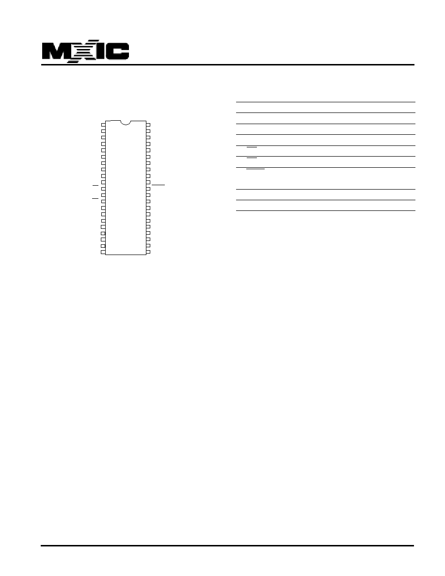
MX29F1615
PIN CONFIGURATIONS
42 PDIP(600mil)
SYMBOL
PIN NAME
A0 - A19
Address Input
Q0 - Q14
Data Input/Output
Q15/A - 1
Q15(Word mode)/LSB addr.(Byte mode)
CE
Chip Enable Input
OE
Output Enable Input
BYTE/VPP
Word/Byte Selection Input/Write Enable
Input
VCC
Power Supply
GND
Ground Pin
PIN DESCRIPTION
MX29F1615
1
2
3
4
5
6
7
8
9
10
11
12
13
14
15
16
17
18
19
20
21
A18
A17
A7
A6
A5
A4
A3
A2
A1
A0
CE
GND
OE
Q0
Q8
Q1
Q9
Q2
Q10
Q3
Q11
42
41
40
39
38
37
36
35
34
33
32
31
30
29
28
27
26
25
24
23
22
A19
A8
A9
A10
A11
A12
A13
A14
A15
A16
BYTE/VPP
GND
Q15/A-1
Q7
Q14
Q6
Q13
Q5
Q12
Q4
VCC
3
P/N: PM0615
REV. 1.1, JUN. 15, 2001
MX29F1615
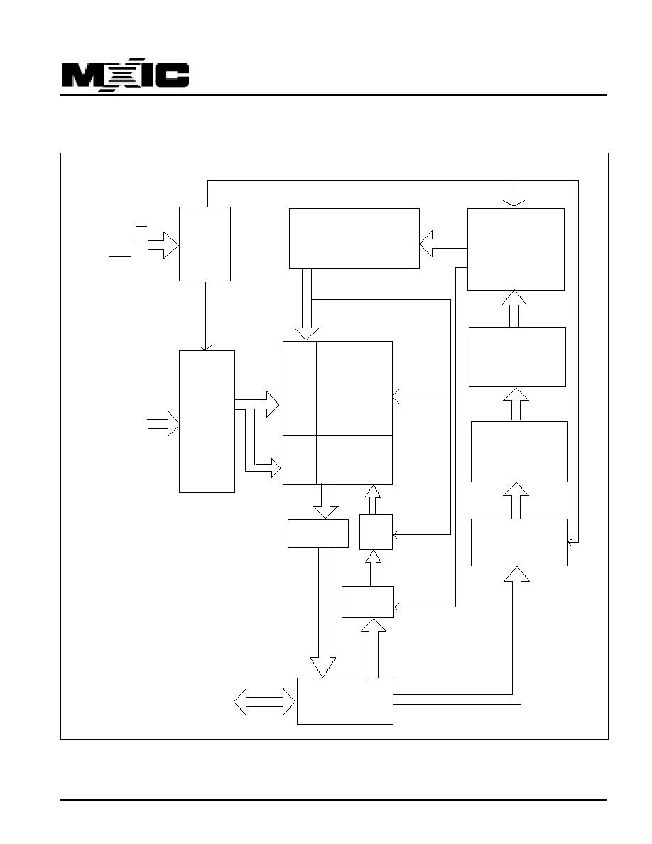
BLOCK DIAGRAM
CONTROL
INPUT
LOGIC
PROGRAM/ERASE
HIGH VOLTAGE
COMMAND INTERFACE
REGISTER
(CIR)
MX29F1615
FLASH
ARRAY
X-DECODER
ADDRESS
LATCH
AND
BUFFER
Y-PASS GATE
Y
-DECODER
ARRAY
SOURCE
HV
COMMAND
DATA
DECODER
COMMAND
DATA LATCH
I/O BUFFER
PGM
DATA
HV
PROGRAM
DATA LATCH
SENSE
AMPLIFIER
Q0-Q15/A-1
Q15/A-1
A0-A19
CE
OE
BYTE/VPP
PAGE
WRITE
STATE
MACHINE
(WSM)
4
P/N: PM0615
REV. 1.1, JUN. 15, 2001
MX29F1615
SYMBOL
TYPE
NAME AND FUNCTION
A0 - A19
INPUT
ADDRESS INPUTS: for memory addresses. Addresses are internally latched
during a write cycle.
Q0 - Q7
INPUT/OUTPUT
LOW-BYTE DATA BUS: Input data and commands during Command Interface
Register(CIR) write cycles. Outputs array,status and identifier data in the
appropriate read mode. Floated when the chip is de-selected or the outputs are
disabled.
Q8 - Q14
INPUT/OUTPUT
HIGH-BYTE DATA BUS: Inputs data during x 16 Data-Write operations. Outputs
array, identifier data in the appropriate read mode; not used for status register
reads. Floated when the chip is de-selected or the outputs are disabled
Q15/A -1
INPUT/OUTPUT
Selects between high-byte data INPUT/OUTPUT(BYTE/VPP = HIGH) and LSB
ADDRESS(BYTE/VPP = LOW) for read operation.
CE
INPUT
CHIP ENABLE INPUTS: Activate the device's control logic, Input buffers,
decoders and sense amplifiers. With CE high, the device is de-selected and
power consumption reduces to Standby level upon completion of any current
program or erase operations. CE must be low to select the device. Device
selection occurs with the latter falling edge of CE. The first rising edge of CE
disables the device.
OE
INPUT
OUTPUT ENABLES: Gates the device's data through the output buffers during a
read cycle OE is active low.
BYTE/VPP
INPUT
BYTE ENABLE: While operating read mode, BYTE/VPP Low places device in x8
mode. All data is then input or output on Q0-7 and Q8-14 float. AddressQ15/A-
1 selects between the high and low byte. While operating read mode, BYTE/VPP
high places the device in x16 mode, and turns off the Q15/A-1 input buffer.
Address A0, then becomes the lowest order address. Write Enable is active while
apply 10V on the BYTE/VPP pin.
VCC
DEVICE POWER SUPPLY(5V
±
10%)
GND
GROUND
Table1.PIN DESCRIPTIONS

5
P/N: PM0615
REV. 1.1, JUN. 15, 2001
MX29F1615
Mode
Notes
CE
OE
BYTE/VPP
A0
A1
A9
Q0-Q7
Q8-Q14
Q15/A-1
Read
1,5
VIL
VIL
VIH/VIL
X
X
X
DOUT
HighZ/DOUT
VIL/VIH/DOUT
Output Disable
1
VIL
VIH
VIH/VIL
X
X
X
High Z
HIghZ
High Z/X
Standby
1
VIH
X
X
X
X
X
X
X
X
Manufacturer ID
2,4
VIL
VIL
VIH/VIL
VIL
VIL
VID
C2H
High Z/00H
VIL/OB
Device ID
2,4
VIL
VIL
VIH/VIL
VIH
VIL
VID
6BH
High Z/00H
VIL/OB
MX29F1615
Write
1,3,6
VIL
VIH
VHH
X
X
X
DIN
DIN
DIN
BUS OPERATION
Flash memory reads, erases and writes in-system via the local CPU . All bus cycles to or from the flash memory conform
to standard microprocessor bus cycles.
NOTES :
1. X can be VIH or VIL for address or control pins.
2. A0 and A1 at VIL provide manufacturer ID codes. A0 at VIH and A1 at VIL provide device ID codes.
3. Commands for different Erase operations or Data program operations can only be successfully completed through proper command
sequence.
4. VID = 11.5V- 12.5V.
5. Q15/A-1 = VIL, Q0 - Q7 =D0-D7 out . Q15/A-1 = VIH, Q0 - Q7 = D8 -D15 out.
6.VHH=9.5V~10.5V
Table2.1 Bus Operations