
4
P/N:PM0629
REV. 1.0, DEC. 20, 1999
MX29F4000
AUTOMATIC PROGRAMMING
The MX29F4000 is byte programmable using the
Automatic Programming algorithm. The Automatic
Programming algorithm makes the external system do
not need to have time out sequence nor to verify the data
programmed. The typical chip programming time at
room temperature of the MX29F4000 is less than 4
seconds.
AUTOMATIC CHIP ERASE
The entire chip is bulk erased using 10 ms erase pulses
according to MXIC's Automatic Chip Erase algorithm.
Typical erasure at room temperature is accomplished in
less than 4 second. The Automatic Erase algorithm
automatically programs the entire array prior to electrical
erase. The timing and verification of electrical erase are
controlled internally within the device.
AUTOMATIC SECTOR ERASE
The MX29F4000 is sector(s) erasable using MXIC's
Auto Sector Erase algorithm. Sector erase modes
allow sectors of the array to be erased in one erase
cycle. The Automatic Sector Erase algorithm
automatically programs the specified sector(s) prior to
electrical erase. The timing and verification of
electrical erase are controlled internally within the
device.
AUTOMATIC PROGRAMMING ALGORITHM
MXIC's Automatic Programming algorithm require the
user to only write program set-up commands (including
2 unlock write cycle and A0H) and a program command
(program data and address). The device automatically
times the programming pulse width, provides the program
verification, and counts the number of sequences. A
status bit similar to DATA polling and a status bit toggling
between consecutive read cycles, provide feedback to
the user as to the status of the programming operation.
AUTOMATIC ERASE ALGORITHM
MXIC's Automatic Erase algorithm requires the user to
write commands to the command register using standard
microprocessor write timings. The device will
automatically pre-program and verify the entire array.
Then the device automatically times the erase pulse
width, provides the erase verification, and counts the
number of sequences. A status bit toggling between
consecutive read cycles provides feedback to the user
as to the status of the programming operation.
Register contents serve as inputs to an internal state-
machine which controls the erase and programming
circuitry. During write cycles, the command register
internally latches address and data needed for the
programming and erase operations. During a system
write cycle, addresses are latched on the falling edge of
WE or CE, whichever happeds later, and data are latched
on the rising edge of WE or CE, whichever happeds first.
MXIC's Flash technology combines years of EPROM
experience to produce the highest levels of quality,
reliability, and cost effectiveness. The MX29F4000
electrically erases all bits simultaneously using Fowler-
Nordheim tunneling. The bytes are programmed by
using the EPROM programming mechanism of hot
electron injection.
During a program cycle, the state-machine will control
the program sequences and command register will not
respond to any command set. During a Sector Erase
cycle, the command register will only respond to Erase
Suspend command. After Erase Suspend is completed,
the device stays in read mode. After the state machine
has completed its task, it will allow the command register
to respond to its full command set.
5
P/N:PM0629
REV. 1.0, DEC. 20, 1999
MX29F4000
First Bus
Second Bus
Third Bus
Fourth Bus
Fifth Bus
Sixth Bus
Command
Bus
Cycle
Cycle
Cycle
Cycle
Cycle
Cycle
Cycle
Addr
Data
Addr
Data
Addr
Data
Addr
Data
Addr
Data
Addr
Data
Reset
1
XXXH
F0H
Read
1
RA
RD
Read Silicon ID
4
555H
AAH
2AAH 55H
555H
90H
ADI
DDI
Sector Protect Verify
4
555H
AAH
2AAH 55H
555H
90H
(SA)X 00H
02
01H
Porgram
4
555H
AAH
2AAH 55H
555H
A0H
PA
PD
Chip Erase
6
555H
AAH
2AAH 55H
555H
80H
555H
AAH
2AAH 55H
555H 10H
Sector Erase
6
555H
AAH
2AAH 55H
555H
80H
555H
AAH
2AAH 55H
SA
30H
Sector Erase Suspend
1
XXXH
B0H
Sector Erase Resume
1
XXXH
30H
Unlock for sector
6
555H
AAH
2AAH 55H
555H
80H
555H
AAH
2AAH 55H
555H 20H
protect/unprotect
TABLE1. SOFTWARE COMMAND DEFINITIONS
Note:
1. ADI = Address of Device identifier; A1=0, A0 = 0 for manufacture code,A1=0, A0 = 1 for device code A2-A18=Do
not care.
(Refer to table 3)
DDI = Data of Device identifier : C2H for manufacture code, 99H for device code.
X = X can be VIL or VIH
RA=Address of memory location to be read.
RD=Data to be read at location RA.
2.PA = Address of memory location to be programmed.
PD = Data to be programmed at location PA.
SA = Address to the sector to be erased.
3.The system should generate the following address patterns: 555H or 2AAH to Address A10~A0 .
Address bit A11~A18=X=Don't care for all address commands except for Program Address (PA) and Sector
Address (SA). Write Sequence may be initiated with A11~A18 in either state.
4.For Sector Protect Verify Operation : If read out data is 01H, it means the sector has been protected.If read out data
is 00H,it means the sector is still not being protected.
COMMAND DEFINITIONS
Device operations are selected by writing specific address
and data sequences into the command register. Writing
incorrect address and data values or writing them in the
improper sequence will reset the device to the read
mode. Table 1 defines the valid register command
sequences. Note that the Erase Suspend (B0H) and
Erase Resume (30H) commands are valid only while the
Sector Erase operation is in progress. Either of the two
reset command sequences will reset the device(when
applicable).
6
P/N:PM0629
REV. 1.0, DEC. 20, 1999
MX29F4000
Mode
Pins
CE
OE
WE
A0
A1
A6
A9
Q0 ~ Q7
Read Silicon ID
L
L
H
L
L
X
V
ID
(2)
C2H
Manfacturer Code(1)
Read Silicon ID
L
L
H
H
L
X
V
ID
(2)
99H
Device Code(1)
Read
L
L
H
A0
A1
A6
A9
D
OUT
Standby
H
X
X
X
X
X
X
HIGH Z
Output Disable
L
H
H
X
X
X
X
HIGH Z
Write
L
H
L
A0
A1
A6
A9
D
IN
(3)
Sector Protect with 12V
L
V
ID
(2)
L
X
X
L
V
ID
(2)
X
system(6)
Chip Unprotect with 12V
L
V
ID
(2)
L
X
X
H
V
ID
(2)
X
system(6)
Verify Sector Protect
L
L
H
X
H
X
V
ID
(2)
Code(5)
with 12V system
Sector Protect without 12V
L
H
L
X
X
L
H
X
system (6)
Chip Unprotect without 12V
L
H
L
X
X
H
H
X
system (6)
Verify Sector Protect/Unprotect
L
L
H
X
H
X
H
Code(5)
without 12V system (7)
Reset
X
X
X
X
X
X
X
HIGH Z
TABLE 2. MX29F4000 BUS OPERATION
NOTES:
1. Manufacturer and device codes may also be accessed via a command register write sequence. Refer to Table 1.
2. VID is the Silicon-ID-Read high voltage, 11.5V to 12.5V.
3. Refer to Table 1 for valid Data-In during a write operation.
4. X can be VIL or VIH.
5. Code=00H means unprotected.
Code=01H means protected.
A18~A16=Sector address for sector protect.
6. Refer to sector protect/unprotect algorithm and waveform.
Must issue "unlock for sector protect/unprotect" command before "sector protect/unprotect without 12V system"
command.
7. The "verify sector protect/unprotect without 12V sysytem" is only following "Sector protect/unprotect without 12V system"
command.

7
P/N:PM0629
REV. 1.0, DEC. 20, 1999
MX29F4000
READ/RESET COMMAND
The read or reset operation is initiated by writing the
read/reset command sequence into the command
register. Microprocessor read cycles retrieve array
data. The device remains enabled for reads until the
command register contents are altered.
If program-fail or erase-fail happen, the write of F0H will
reset the device to abort the operation. A valid command
must then be written to place the device in the desired
state.
SILICON-ID-READ COMMAND
Flash memories are intended for use in applications
where the local CPU alters memory contents. As such,
manufacturer and device codes must be accessible
while the device resides in the target system. PROM
programmers typically access signature codes by raising
A9 to a high voltage. However, multiplexing high voltage
onto address lines is not generally desired system
design practice.
The MX29F4000 contains a Silicon-ID-Read operation to
supplement traditional PROM programming
methodology. The operation is initiated by writing the
read silicon ID command sequence into the command
register. Following the command write, a read cycle with
A1=VIL,A0=VIL retrieves the manufacturer code of C2H.
A read cycle with A1=VIL, A0=VIH returns the device
code of 99H for MX29F4000.
SET-UP AUTOMATIC CHIP/SECTOR ERASE
Chip erase is a six-bus cycle operation. There are two
"unlock" write cycles. These are followed by writing the
"set-up" command 80H. Two more "unlock" write cycles
are then followed by the chip erase command 10H.
The Automatic Chip Erase does not require the device
to be entirely pre-programmed prior to executing the
Automatic Chip Erase. Upon executing the Automatic
Chip Erase, the device will automatically program and
verify the entire memory for an all-zero data pattern.
When the device is automatically verified to contain an
all-zero pattern, a self-timed chip erase and verify begin.
The erase and verify operations are completed when the
data on Q7 is "1" at which time the device returns to the
Read mode. The system is not required to provide any
control or timing during these operations.
When using the Automatic Chip Erase algorithm, note
that the erase automatically terminates when adequate
erase margin has been achieved for the memory array(no
erase verification command is required).
If the Erase operation was unsuccessful, the data on Q5
is "1"(see Table 4), indicating the erase operation exceed
internal timing limit.
The automatic erase begins on the rising edge of the last
WE or CE, whichever happeds first pulse in the command
sequence and terminates when the data on Q7 is "1" and
the data on Q6 stops toggling for two consecutive read
cycles, at which time the device returns to the Read
mode.
Pins
A0
A1
Q7
Q6
Q5
Q4
Q3
Q2
Q1
Q0
Code(Hex)
Manufacture code
VIL
VIL
1
1
0
0
0
0
1
0
C2H
Device code for MX29F4000
VIH
VIL
1
0
1
0
0
0
1
1
99H
Sector Protection Verification
X
VIH
0
0
0
0
0
0
0
1
01H(Protected)
X
VIH
0
0
0
0
0
0
0
0
00H(Unprotected)
TABLE 3. EXPANDED SILICON ID CODE
8
P/N:PM0629
REV. 1.0, DEC. 20, 1999
MX29F4000
SECTOR ERASE COMMANDS
The Automatic Sector Erase does not require the
device to be entirely pre-programmed prior to
executing the Automatic Set-up Sector Erase
command and Automatic Sector Erase command.
Upon executing the Automatic Sector Erase
command, the device will automatically program and
verify the sector(s) memory for an all-zero data
pattern. The system is not required to provide any
control or timing during these operations.
When the sector(s) is automatically verified to contain
an all-zero pattern, a self-timed sector erase and
verify begin. The erase and verify operations are
complete when the data on Q7 is "1" and the data on
Q6 stops toggling for two consecutive read cycles, at
which time the device returns to the Read mode. The
system is not required to provide any control or timing
during these operations.
When using the Automatic Sector Erase algorithm,
note that the erase automatically terminates when
adequate erase margin has been achieved for the
memory array (no erase verification command is
required). Sector erase is a six-bus cycle operation.
There are two "unlock" write cycles. These are
followed by writing the set-up command 80H. Two
more "unlock" write cycles are then followed by the
sector erase command 30H. The sector address is
latched on the falling edge of WE or CE, whichever
happeds later, while the command(data) is latched on
the rising edge of WE or CE, whichever happeds first.
Sector addresses selected are loaded into internal
register on the sixth falling edge of WE or CE,
whichever happeds later. Each successive sector load
cycle started by the falling edge of WE or CE,
whichever happeds later must begin within 30us from
the rising edge of the preceding WE or CE, whichever
happeds first. Otherwise, the loading period ends and
internal auto sector erase cycle starts. (Monitor Q3 to
determine if the sector erase timer window is still
open, see section Q3, Sector Erase Timer.) Any
command other than Sector Erase(30H) or Erase
Suspend(B0H) during the time-out period resets the
device to read mode.
Status
Q7
Q6
Q5
Q3
Q2
Note1
Note2
Byte Program in Auto Program Algorithm
Q7
Toggle
0
N/A
No Toggle
Auto Erase Algorithm
0
Toggle
0
1
Toggle
Erase Suspend Read
1
No
0
N/A
Toggle
In Progress
(Erase Suspended Sector)
Toggle
Erase Suspended Mode
Erase Suspend Read
Data
Data
Data
Data
Data
(Non-Erase Suspended Sector)
Erase Suspend Program
Q7
Toggle
0
N/A
N/A
Byte Program in Auto Program Algorithm
Q7
Toggle
1
N/A
No Toggle
Exceeded
Auto Erase Algorithm
0
Toggle
1
1
Toggle
Time Limits Erase Suspend Program
Q7
Toggle
1
N/A
N/A
Table 4. Write Operation Status
Note:
1. Q7 and Q2 require a valid address when reading status information. Refer to the appropriate subsection for further
details.
2. Q5 switches to '1' when an Auto Program or Auto Erase operation has exceeded the maximum timing limits.
See "Q5:Exceeded Timing Limits " for more information.

9
P/N:PM0629
REV. 1.0, DEC. 20, 1999
MX29F4000
ERASE SUSPEND
This command only has meaning while the state machine
is executing Automatic Sector Erase operation, and
therefore will only be responded during Automatic Sector
Erase operation. However, When the Erase Suspend
command is written during the sector erase time-out, the
device immediately terminates the time-out period and
suspends the erase operation. After this command has
been executed, the command register will initiate erase
suspend mode. The state machine will return to read
mode automatically after suspend is ready. At this time,
state machine only allows the command register to
respond to the Read Memory Array, Erase Resume and
program commands.
The system can determine the status of the program
operation using the Q7 or Q6 status bits, just as in the
standard program operation. After an erase-suspend
program operation is complete, the system can once
again read array data within non-suspended sectors.
ERASE RESUME
This command will cause the command register to clear
the suspend state and return back to Sector Erase mode
but only if an Erase Suspend command was previously
issued. Erase Resume will not have any effect in all
other conditions.Another Erase Suspend command can
be written after the chip has resumed erasing.
SET-UP AUTOMATIC PROGRAM
COMMANDS
To initiate Automatic Program mode, A three-cycle
command sequence is required. There are two "unlock"
write cycles. These are followed by writing the Automatic
Program command A0H.
Once the Automatic Program command is initiated, the
next WE or CE pulse causes a transition to an active
programming operation. Addresses are latched on the
falling edge, and data are internally latched on the rising
edge of the WE or CE, whichever happeds first pulse.
The rising edge of WE or CE, whichever happeds first
also begins the programming operation. The system is
not required to provide further controls or timings. The
device will automatically provide an adequate internally
generated program pulse and verify margin.
If the program opetation was unsuccessful, the data on
Q5 is "1"(see Table 4), indicating the program operation
exceed internal timing limit. The automatic programming
operation is completed when the data read on Q6 stops
toggling for two consecutive read cycles and the data on
Q7 and Q6 are equivalent to data written to these two
bits, at which time the device returns to the Read
mode(no program verify command is required).
DATA POLLING-Q7
The MX29F4000 also features Data Polling as a method
to indicate to the host system that the Automatic Program
or Erase algorithms are either in progress or completed.
While the Automatic Programming algorithm is in
operation, an attempt to read the device will produce the
complement data of the data last written to Q7. Upon
completion of the Automatic Program Algorithm an
attempt to read the device will produce the true data last
written to Q7. The Data Polling feature is valid after the
rising edge of the fourth WE or CE, whichever happeds
first pulse of the four write pulse sequences for automatic
program.
While the Automatic Erase algorithm is in operation, Q7
will read "0" until the erase operation is competed. Upon
completion of the erase operation, the data on Q7 will
read "1". The Data Polling feature is valid after the rising
edge of the sixth WE or CE, whichever happeds first
pulse of six write pulse sequences for automatic chip/
sector erase.
The Data Polling feature is active during Automatic
Program/Erase algorithm or sector erase time-out.(see
section Q3 Sector Erase Timer)

10
P/N:PM0629
REV. 1.0, DEC. 20, 1999
MX29F4000
Q2 toggles when the system reads at addresses within
those sectors that have been selected for erasure. (The
system may use either OE or CE to control the read
cycles.) But Q2 cannot distinguish whether the sector is
actively erasing or is erase-suspended. Q6, by
comparison, indicates whether the device is actively
erasing, or is in Erase Suspend, but cannot distinguish
which sectors are selected for erasure. Thus, both
status bits are required for sectors and mode information.
Refer to Table 4 to compare outputs for Q2 and Q6.
Reading Toggle Bits Q6/ Q2
Whenever the system initially begins reading toggle bit
status, it must read Q7-Q0 at least twice in a row to
determine whether a toggle bit is toggling. Typically, the
system would note and store the value of the toggle bit
after the first read. After the second read, the system
would compare the new value of the toggle bit with the
first. If the toggle bit is not toggling, the device has
completed the program or erase operation. The system
can read array data on Q7-Q0 on the following read
cycle.
However, if after the initial two read cycles, the system
determines that the toggle bit is still toggling, the system
also should note whether the value of Q5 is high (see the
section on Q5). If it is, the system should then determine
again whether the toggle bit is toggling, since the toggle
bit may have stopped toggling just as Q5 went high. If
the toggle bit is no longer toggling, the device has
successfuly completed the program or erase operation.
If it is still toggling, the device did not complete the
operation successfully, and the system must write the
reset command to return to reading array data.
The remaining scenario is that system initially determines
that the toggle bit is toggling and Q5 has not gone high.
The system may continue to monitor the toggle bit and
Q5 through successive read cycles, determining the
status as described in the previous paragraph.
Alternatively, it may choose to perform other system
tasks. In this case, the system must start at the beginning
of the algorithm when it returns to determine the status
of the operation.
Q6:Toggle BIT I
Toggle Bit I on Q6 indicates whether an Automatic
Program or Erase algorithm is in progress or complete,
or whether the device has entered the Erase Suspend
mode. Toggle Bit I may be read at any address, and is
valid after the rising edge of the final WE or CE, whichever
happeds first pulse in the command sequence(prior to the
program or erase operation), and during the sector time-
out.
During an Automatic Program or Erase algorithm
operation, successive read cycles to any address cause
Q6 to toggle. The system may use either OE or CE to
control the read cycles. When the operation is complete,
Q6 stops toggling.
After an erase command sequence is written, if all
sectors selected for erasing are protected, Q6 toggles
and returns to reading array data. If not all selected
sectors are protected, the Automatic Erase algorithm
erases the unprotected sectors, and ignores the selected
sectors that are protected.
The system can use Q6 and Q2 together to determine
whether a sector is actively erasing or is erase suspended.
When the device is actively erasing (that is, the Automatic
Erase algorithm is in progress), Q6 toggling. When the
device enters the Erase Suspend mode, Q6 stops
toggling. However, the system must also use Q2 to
determine which sectors are erasing or erase-suspended.
Alternatively, the system can use Q7.
If a program address falls within a protected sector, Q6
toggles for approximately 2us after the program command
sequence is written, then returns to reading array data.
Q6 also toggles during the erase-suspend-program
mode, and stops toggling once the Automatic Program
algorithm is complete.
Table 4 shows the outputs for Toggle Bit I on Q6.
Q2:Toggle Bit II
The "Toggle Bit II" on Q2, when used with Q6, indicates
whether a particular sector is actively eraseing (that is,
the Automatic Erase alorithm is in process), or whether
that sector is erase-suspended. Toggle Bit I is valid after
the rising edge of the final WE or CE, whichever happeds
first pulse in the command sequence.

11
P/N:PM0629
REV. 1.0, DEC. 20, 1999
MX29F4000
Q5
Q3
Exceeded Timing Limits
Q5 will indicate if the program or erase time has exceeded
the specified limits(internal pulse count). Under these
conditions Q5 will produce a "1". This time-out condition
indicates that the program or erase cycle was not
successfully completed. Data Polling and Toggle Bit are
the only operating functions of the device under this
condition.
If this time-out condition occurs during sector erase
operation, it specifies that a particular sector is bad and
it may not be reused. However, other sectors are still
functional and may be used for the program or erase
operation. The device must be reset to use other
sectors. Write the Reset command sequence to the
device, and then execute program or erase command
sequence. This allows the system to continue to use the
other active sectors in the device.
If this time-out condition occurs during the chip erase
operation, it specifies that the entire chip is bad or
combination of sectors are bad.
If this time-out condition occurs during the byte
programming operation, it specifies that the entire sector
containing that byte is bad and this sector maynot be
reused, (other sectors are still functional and can be
reused).
The time-out condition may also appear if a user tries to
program a non blank location without erasing. In this
case the device locks out and never completes the
Automatic Algorithm operation. Hence, the system
never reads a valid data on Q7 bit and Q6 never stops
toggling. Once the Device has exceeded timing limits,
the Q5 bit will indicate a "1". Please note that this is not
a device failure condition since the device was incorrectly
used.
DATA PROTECTION
The MX29F4000 is designed to offer protection against
accidental erasure or programming caused by spurious
system level signals that may exist during power
transition. During power up the device automatically
resets the state machine in the Read mode. In addition,
Sector Erase Timer
After the completion of the initial sector erase command
sequence, the sector erase time-out will begin. Q3 will
remain low until the time-out is complete. Data Polling
and Toggle Bit are valid after the initial sector erase
command sequence.
If Data Polling or the Toggle Bit indicates the device has
been written with a valid erase command, Q3 may be
used to determine if the sector erase timer window is still
open. If Q3 is high ("1") the internally controlled erase
cycle has begun; attempts to write subsequent
commands to the device will be ignored until the erase
operation is completed as indicated by Data Polling or
Toggle Bit. If Q3 is low ("0"), the device will accept
additional sector erase commands. To insure the
command has been accepted, the system software
should check the status of Q3 prior to and following each
subsequent sector erase command. If Q3 were high on
the second status check, the command may not have
been accepted.
WRITE PULSE "GLITCH" PROTECTION
Noise pulses of less than 5ns(typical) on CE or WE will
not initiate a write cycle.
LOGICAL INHIBIT
Writing is inhibited by holding any one of OE = VIL, CE
= VIH or WE = VIH. To initiate a write cycle CE and WE
must be a logical zero while OE is a logical one.
POWER SUPPLY DECOUPLING
In order to reduce power switching effect, each device
should have a 0.1uF ceramic capacitor connected
between its VCC and GND.
with its control register architecture, alteration of the
memory contents only occurs after successful completion
of specific command sequences. The device also
incorporates several features to prevent inadvertent
write cycles resulting from VCC power-up and power-
down transition or system noise.

12
P/N:PM0629
REV. 1.0, DEC. 20, 1999
MX29F4000
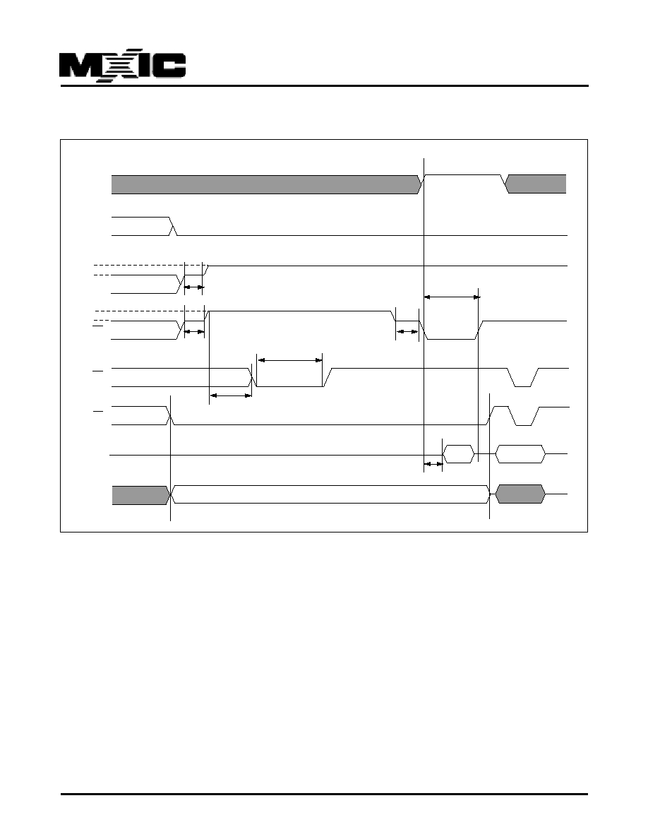
SECTOR PROTECTION WITH 12V SYSTEM
The MX29F4000 features sector protection. This feature
will disable both program and erase operations for these
sectors protected. To activate this mode, the
programming equipment must force VID on address pin
A9 and control pin OE, (suggest VID = 12V) A6 = VIL and
CE = VIL.(see Table 2) Programming of the protection
circuitry begins on the falling edge of the WE or CE,
whichever happeds later pulse and is terminated on the
rising edge. Please refer to sector protect algorithm and
waveform.
To verify programming of the protection circuitry, the
programming equipment must force VID on address pin
A9 ( with CE and OE at VIL and WE at VIH). When A1=1,
it will produce a logical "1" code at device output Q0 for
a protected sector. Otherwise the device will produce
00H for the unprotected sector. In this mode, the
addresses, except for A1, are don't care. Address
locations with A1 = VIL are reserved to read manufacturer
and device codes.(Read Silicon ID)
It is also possible to determine if the sector is protected
in the system by writing a Read Silicon ID command.
Performing a read operation with A1=VIH, it will produce
a logical "1" at Q0 for the protected sector.
CHIP UNPROTECT WITH 12V SYSTEM
The MX29F4000 also features the chip unprotect mode,
so that all sectors are unprotected after chip unprotect
is completed to incorporate any changes in the code. It
is recommended to protect all sectors before activating
chip unprotect mode.
To activate this mode, the programming equipment
must force VID on control pin OE and address pin A9.
The CE pins must be set at VIL. Pins A6 must be set to
VIH.(see Table 2) Refer to chip unprotect algorithm and
waveform for the chip unprotect algorithm. The
unprotection mechanism begins on the falling edge of
the WE or CE, whichever happeds later, pulse and is
terminated on the rising edge.
POWER-UP SEQUENCE
The MX29F4000 powers up in the Read only mode. In
addition, the memory contents may only be altered after
successful completion of the predefined command
sequences.
SECTOR PROTECTION WITHOUT 12V
SYSTEM
The MX29F4000 also feature a sector protection method
in a system without 12V power suppply. The programming
equipment do not need to supply 12 volts to protect
sectors. The details are shown in sector protect algorithm
and waveform.
CHIP UNPROTECT WITHOUT 12V SYSTEM
The MX29F4000 also feature a chip unprotection method
in a system without 12V power supply. The programming
equipment do not need to supply 12 volts to unprotect all
sectors. The details are shown in chip unprotect algorithm
and waveform.
It is also possible to determine if the chip is unprotected
in the system by writing the Read Silicon ID command.
Performing a read operation with A1=VIH, it will produce
00H at data outputs(Q0-Q7) for an unprotected sector.
It is noted that all sectors are unprotected after the chip
unprotect algorithm is completed.
13
P/N:PM0629
REV. 1.0, DEC. 20, 1999
MX29F4000
29F4000-55
(note2)
29F4000-70
29F4000-90
29F4000-12
Symbol PARAMETER
MIN.
MAX.
MIN. MAX. MIN. MAX.
MIN. MAX.
Unit
Conditions
tACC
Address to Output Delay
55
70
90
120
ns
CE=OE=VIL
tCE
CE to Output Delay
55
70
90
120
ns
OE=VIL
tOE
OE to Output Delay
30
40
40
50
ns
CE=VIL
tDF
OE High to Output Float
(
Note1) 0
30
0
30
0
40
0
40
ns
CE=VIL
tOH
Address to Output hold
0
0
0
0
ns
CE=OE=VIL
NOTE:
1. tDF is defined as the time at which the output achieves the
open circuit condition and data is no longer driven.
2.Under condition of VCC=5V
�
10%,CL=50pF,VIH/VIL=3.0/
0V,VOH/VOL=1.5/1.5V,IOL=2mA,IOH=-2mA.
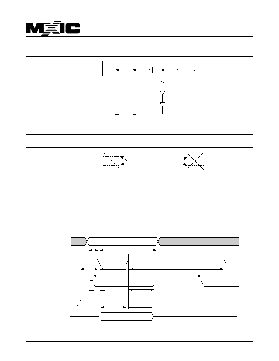
TEST CONDITIONS:
� Input pulse levels: 0.45V/2.4V
� Input rise and fall times is equal to or less than 0ns
� Output load: 1 TTL gate + 100pF (Including scope and jig)
� Reference levels for measuring timing: 0.8V, 2.0V
NOTES:
1. VIL min. = -1.0V for pulse width is equal to or less than
50 ns.
VIL min. = -2.0V for pulse width is equal to or less than 20 ns.
2. VIH max. = VCC + 1.5V for pulse width is equal to or less
than 20 ns.
If VIH is over the specified maximum value, read operation
cannot be guaranteed.
READ OPERATION
DC CHARACTERISTICS (TA = 0
�
C TO 70
�
C, VCC = 5V�10%)
SYMBOL
PARAMETER
MIN.
TYP
MAX.
UNIT
CONDITIONS
ILI
Input Leakage Current
1
uA
VIN = GND to VCC
ILO
Output Leakage Current
10
uA
VOUT = GND to VCC
ISB1
Standby VCC current
1
mA
CE = VIH
ISB2
1
5
uA
CE = VCC + 0.3V
ICC1
Operating VCC current
30
mA
IOUT = 0mA, f=5MH
ICC2
50
mA
IOUT = 0mA, f=10MHz
VIL
Input Low Voltage
-0.3
(NOTE 1)
0.8
V
VIH
Input High Voltage
2.0
VCC + 0.3
V
VOL
Output Low Voltage
0.45
V
IOL = 2.1mA
VOH1
Output High Voltage(TTL)
2.4
V
IOH = -2mA
VOH2
Output High Voltage(CMOS)
VCC-0.4
V
IOH = -100uA,VCC=VCC MIN
CAPACITANCE (TA = 25
o
C, f = 1.0 MHz)
SYMBOL
PARAMETER
MIN.
TYP
MAX.
UNIT
CONDITIONS
CIN1
Input Capacitance
8
pF
VIN = 0V
CIN2
Control Pin Capacitance
12
pF
VIN = 0V
COUT
Output Capacitance
12
pF
VOUT = 0V
AC CHARACTERISTICS (TA = 0
o
C to 70
o
C, VCC = 5V
�
�
�
�
�
10%)

14
P/N:PM0629
REV. 1.0, DEC. 20, 1999
MX29F4000
ABSOLUTE MAXIMUM RATINGS
RATING
VALUE
Ambient Operating Temperature
0
o
C to 70
o
C
Storage Temperature
-65
o
C to 125
o
C
Applied Input Voltage
-0.5V to 7.0V
Applied Output Voltage
-0.5V to 7.0V
VCC to Ground Potential
-0.5V to 7.0V
A9 & OE
-0.5V to 13.5V
NOTICE:
Stresses greater than those listed under ABSOLUTE
MAXIMUM RATINGS may cause permanent damage to
the device. This is a stress rating only and functional
operational sections of this specification is not implied.
Exposure to absolute maximum rating conditions for
extended period may affect reliability.
NOTICE:
Specifications contained within the following tables are
subject to change.
READ TIMING WAVEFORMS
Addresses
CE
OE
tACC
WE
VIH
VIL
VIH
VIL
VIH
VIL
VIH
VIL
VOH
VOL
HIGH Z
HIGH Z
DATA Valid
tOE
tDF
tCE
Outputs
tOH
ADD Valid
NOTES:
1. VIL min. = -0.6V for pulse width is equal to or less than
20ns.
2. If VIH is over the specified maximum value, programming
operation cannot be guranteed.
3. ICCES is specified with the device de-selected. If the
device is read during erase suspend mode, current draw is
the sum of ICCES and ICC1 or ICC2.
4. All current are in RMS unless otherwise noted.
DC CHARACTERISTICS (TA = 0
o
C to 70
o
C, VCC = 5V
�
�
�
�
�
10%)
SYMBOL
PARAMETER
MIN.
TYP
MAX.
UNIT
CONDITIONS
ICC1 (Read)
Operating VCC Current
30
mA
IOUT=0mA, f=5MHz
ICC2
50
mA
IOUT=0mA, F=10MHz
ICC3 (Program)
50
mA
In Programming
ICC4 (Erase)
50
mA
In Erase
ICCES
VCC Erase Suspend Current
2
mA
CE=VIH, Erase Suspended
COMMAND PROGRAMMING/DATA PROGRAMMING/ERASE OPERATION
15
P/N:PM0629
REV. 1.0, DEC. 20, 1999
MX29F4000
AC CHARACTERISTICS TA = 0
o
C to 70
o
C, VCC = 5V
�
�
�
�
�
10%
29F4000-55
(Note2)
29F4000-70
29F4000-90
29F4000-12
SYMBOL PARAMETER
MIN.
MAX. MIN.
MAX. MIN.
MAX.
MIN.
MAX.
Unit
tOES
OE setup time
50
50
50
50
ns
tCWC
Command programming cycle
70
70
90
120
ns
tCEP
WE programming pulse width
45
45
45
50
ns
tCEPH1
WE programming pluse width High
20
20
20
20
ns
tCEPH2
WE programming pluse width High
20
20
20
20
ns
tAS
Address setup time
0
0
0
0
ns
tAH
Address hold time
45
45
45
50
ns
tDS
Data setup time
30
30
45
50
ns
tDH
Data hold time
0
0
0
0
ns
tCESC
CE setup time before command write
0
0
0
0
ns
tDF
Output disable time (Note 1)
30
30
40
40
ns
tAETC
Total erase time in auto chip erase
4(TYP.)
32
4(TYP.)
32
4(TYP.) 32
4(TYP.) 32
s
tAETB
Total erase time in auto sector erase
1.3(TYP.)10.4
1.3(TYP.) 10.4
1.3(TYP.)10.4
1.3(TYP.)10.4
s
tAVT
Total programming time in auto verify
7
210
7
210
7
210
7
210
us
tBAL
Sector address load time
100
100
100
100
us
tCH
CE Hold Time
0
0
0
0
ns
tCS
CE setup to WE going low
0
0
0
0
ns
tVLHT
Voltge Transition Time
4
4
4
4
us
tOESP
OE Setup Time to WE Active
4
4
4
4
us
tWPP1
Write pulse width for sector protect
10
10
10
10
us
tWPP2
Write pulse width for sector unprotect
12
12
12
12
ms
NOTES:
1. tDF defined as the time at which the output achieves the open circuit condition and data is no longer driven.
2.Under conditions of VCC=5V
�
10%,CL=50pF,VIH/VIL=3.0/0V,VOL/VOH=1.5/1.5, IOL=2mA,IOH=-2mA.
16
P/N:PM0629
REV. 1.0, DEC. 20, 1999
MX29F4000
SWITCHING TEST CIRCUITS
SWITCHING TEST WAVEFORMS
COMMAND WRITE TIMING WAVEFORM
Addresses
CE
OE
WE
DIN
tDS
tAH
Data
tDH
tCS
tCH
tCWC
tCEPH1
tCEP
tOES
tAS
VCC
5V
VIH
VIL
VIH
VIL
VIH
VIL
VIH
VIL
VIH
VIL
ADD Valid
DEVICE UNDER
TEST
DIODES=IN3064
OR EQUIVALENT
CL
1.2K ohm
1.6K ohm
+5V
CL=100pF Including jig capacitance
CL= 50pF for 29F4000-55
2.0V
2.0V
0.8V
0.8V
TEST POINTS
2.4V
0.45V
AC TESTING: Inputs are driven at 2.4V for a logic "1" and 0.45V for a logic "0".
Input pulse rise and fall times are < 20ns.(5ns for 29F4000-55)
Note:VIH/VIL=3.0/0V,VOH/VOL=1.5/1.5V for 29F4000-55
OUTPUT
INPUT
17
P/N:PM0629
REV. 1.0, DEC. 20, 1999
MX29F4000
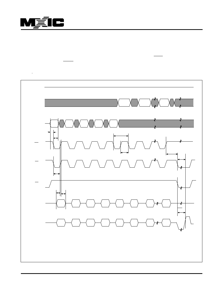
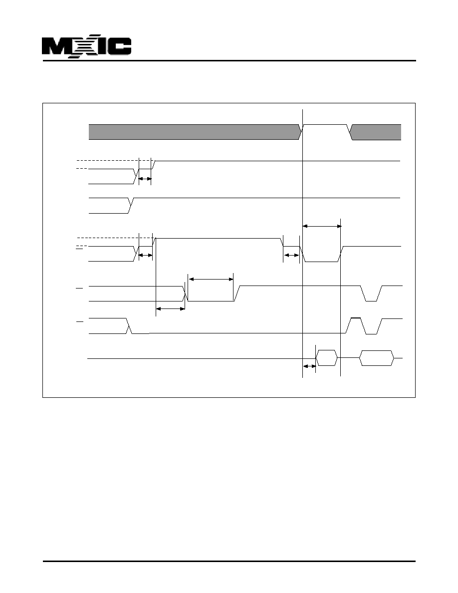
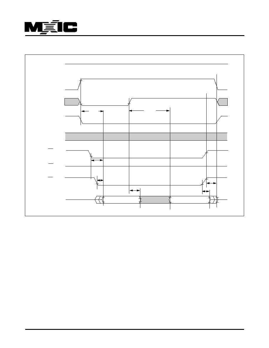
One byte data is programmed. Verify in fast algorithm
and additional programming by external control are not
required because these operations are executed
automatically by internal control circuit. Programming
completion can be verified by DATA polling and toggle
AUTOMATIC PROGRAMMING TIMING WAVEFORM
bit checking after automatic verification starts. Device
outputs DATA during programming and DATA after
programming on Q7.(Q6 is for toggle bit; see toggle bit,
DATA polling, timing waveform)
AUTOMATIC PROGRAMMING TIMING WAVEFORM
tCWC
tAS
tCEP
tDS
tDH
tDF
Vcc 5V
CE
OE
Q0,Q1,Q2
Q4(Note 1)
WE
A11~A18
tCEPH1
tAH
ADD Valid
tCESC
Q7
Command In
ADD Valid
A0~A10
Command In
Command In
Data In
DATA
Command In
Command In
Command In
Data In
DATA
DATA
tAVT
tOE
DATA polling
2AAH
555H
555H
(Q0~Q7)
Command #55H
Command #A0H
Notes:
(1). Q6:Toggle bit, Q5:Timing-limit bit, Q3: Time-out bit
Command #AAH
18
P/N:PM0629
REV. 1.0, DEC. 20, 1999
MX29F4000
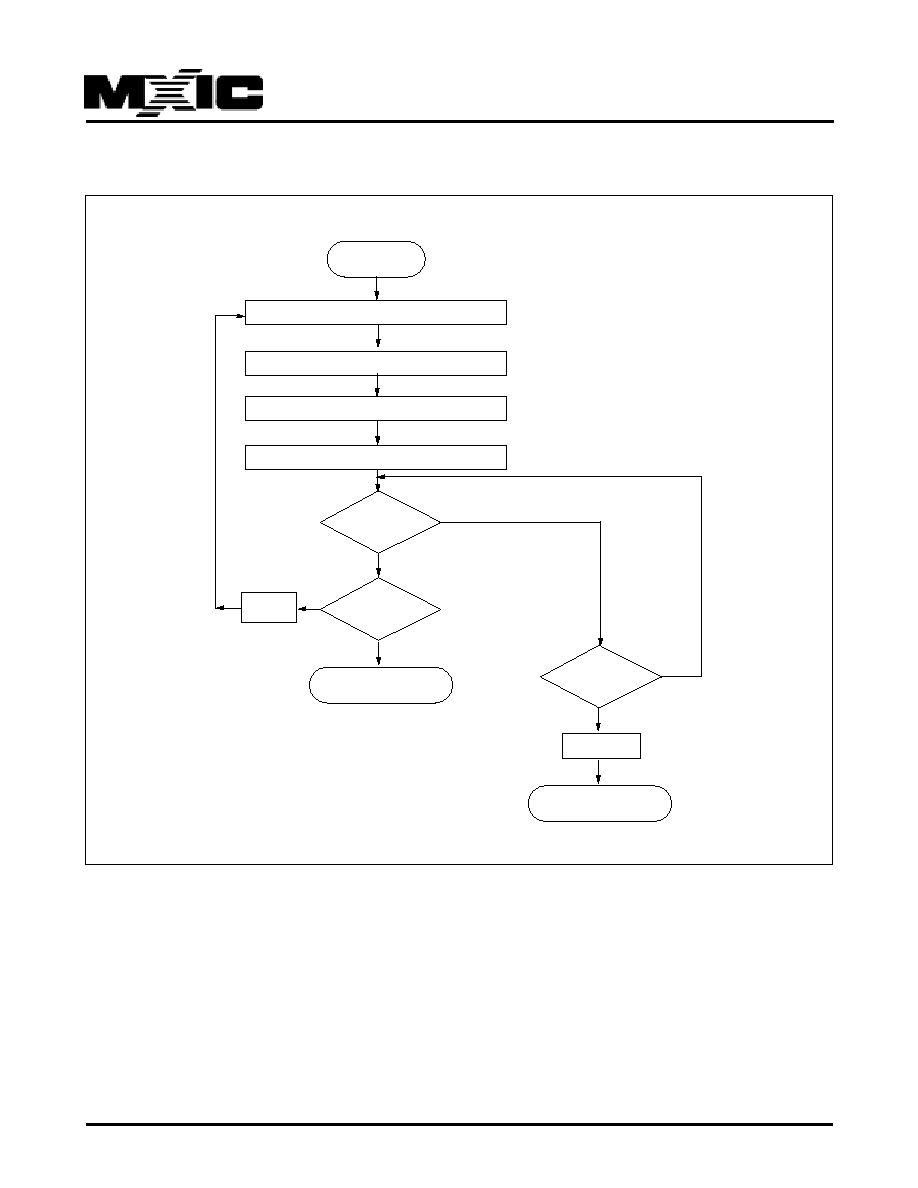
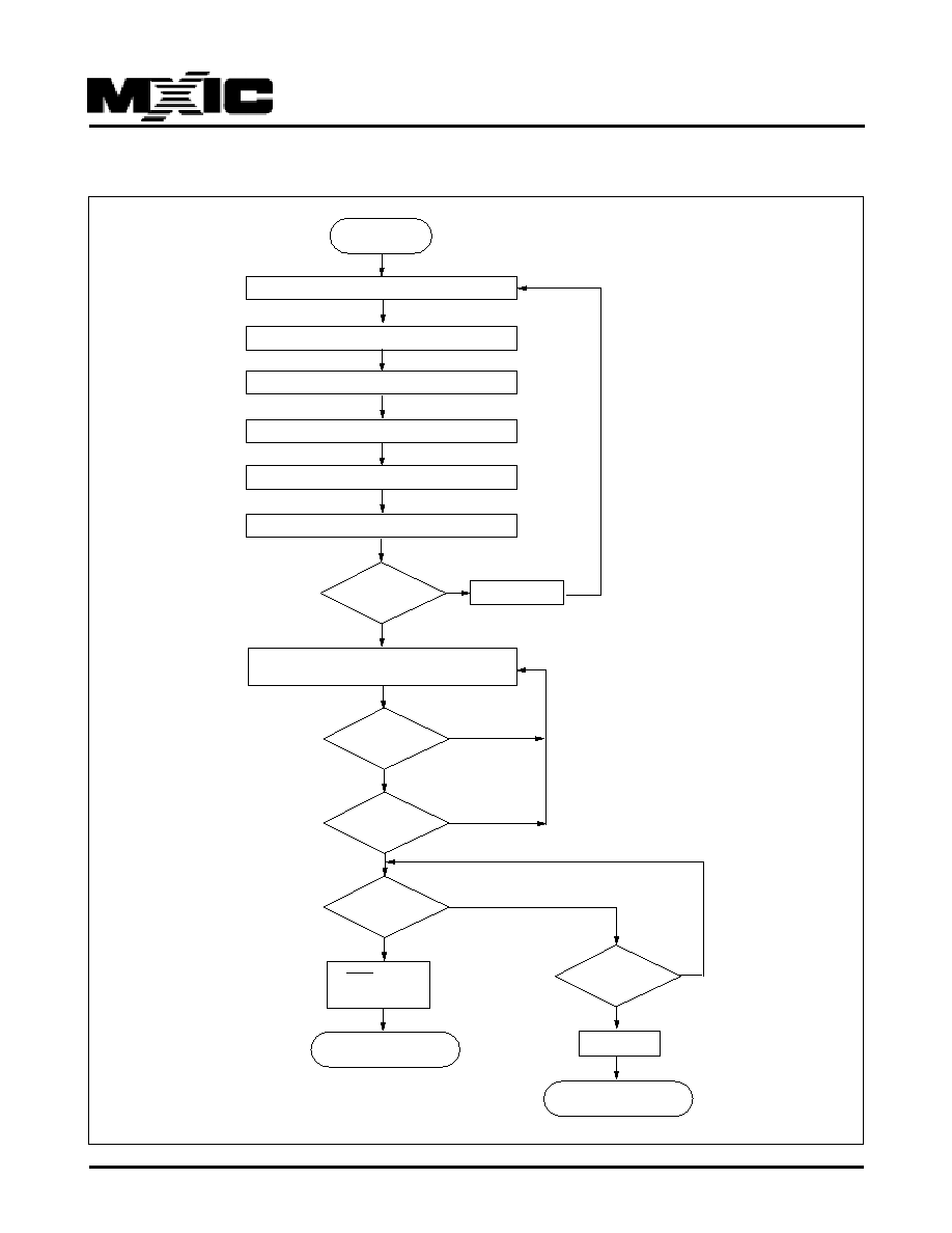
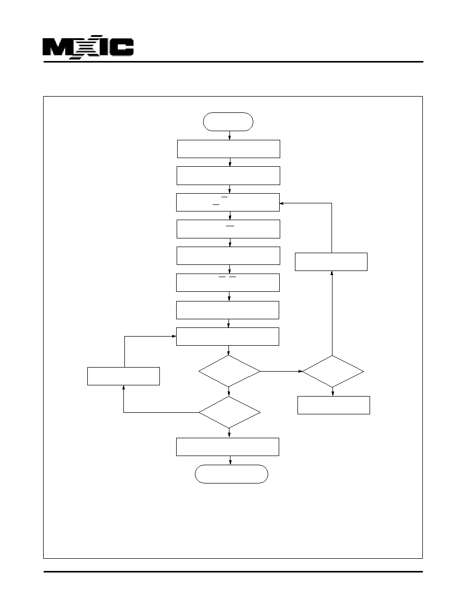
AUTOMATIC PROGRAMMING ALGORITHM FLOWCHART
START
Write Data AAH Address 555H
Write Data 55H Address 2AAH
Write Program Data/Address
Write Data A0H Address 555H
YES
NO
Toggle Bit Checking
Q6 not Toggled
Verify Byte Ok
YES
Q5 = 1
Reset
Auto Program Completed
Auto Program Exceed
Timing Limit
NO
Invalid
Command
YES
NO

19
P/N:PM0629
REV. 1.0, DEC. 20, 1999
MX29F4000
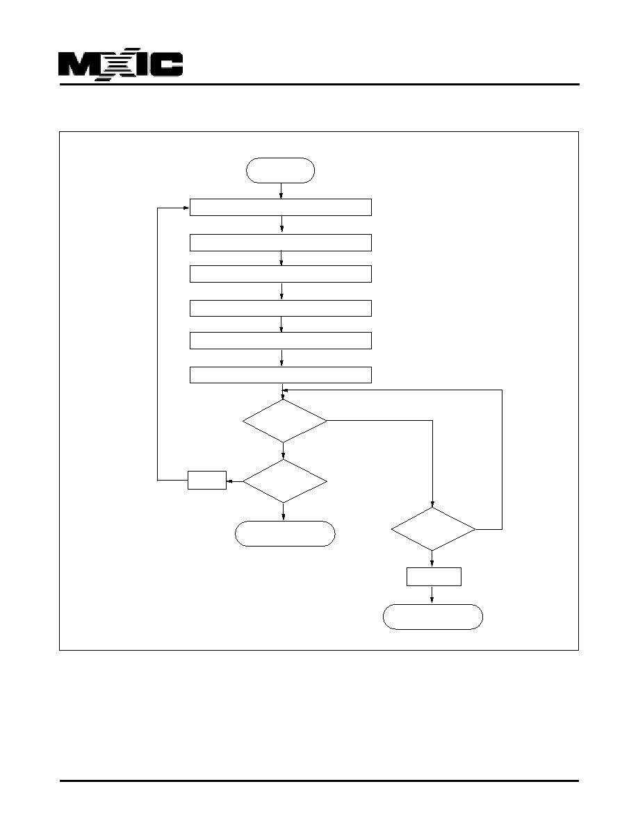
All data in chip are erased. External erase verification is
not required because data is erased automatically by
internal control circuit. Erasure completion can be
verified by DATA polling and toggle bit checking after
automatic erase starts. Device outputs 0 during erasure
and 1 after erasure on Q7.(Q6 is for toggle bit; see toggle
bit, DATA polling, timing waveform)
AUTOMATIC CHIP ERASE TIMING WAVEFORM
AUTOMATIC CHIP ERASE TIMING WAVEFORM
tCWC
tAS
tCEP
tDS tDH
Vcc 5V
CE
OE
Q0,Q1,
Q4(Note 1)
WE
A11~A18
tCEPH1
tAH
Q7
Command In
A0~A10
Command In
Command In
Command In
Command In
Command In
tAETC
DATA polling
2AAH
555H
555H
Command #AAH
Command #55H
Command #80H
(Q0~Q7)
Notes:
(1). Q6:Toggle bit, Q5:Timing-limit bit, Q3: Time-out bit, Q2: Toggle bit
555H
2AAH
555H
Command In
Command In
Command #AAH
Command In
Command In
Command #55H
Command In
Command In
Command #10H
20
P/N:PM0629
REV. 1.0, DEC. 20, 1999
MX29F4000
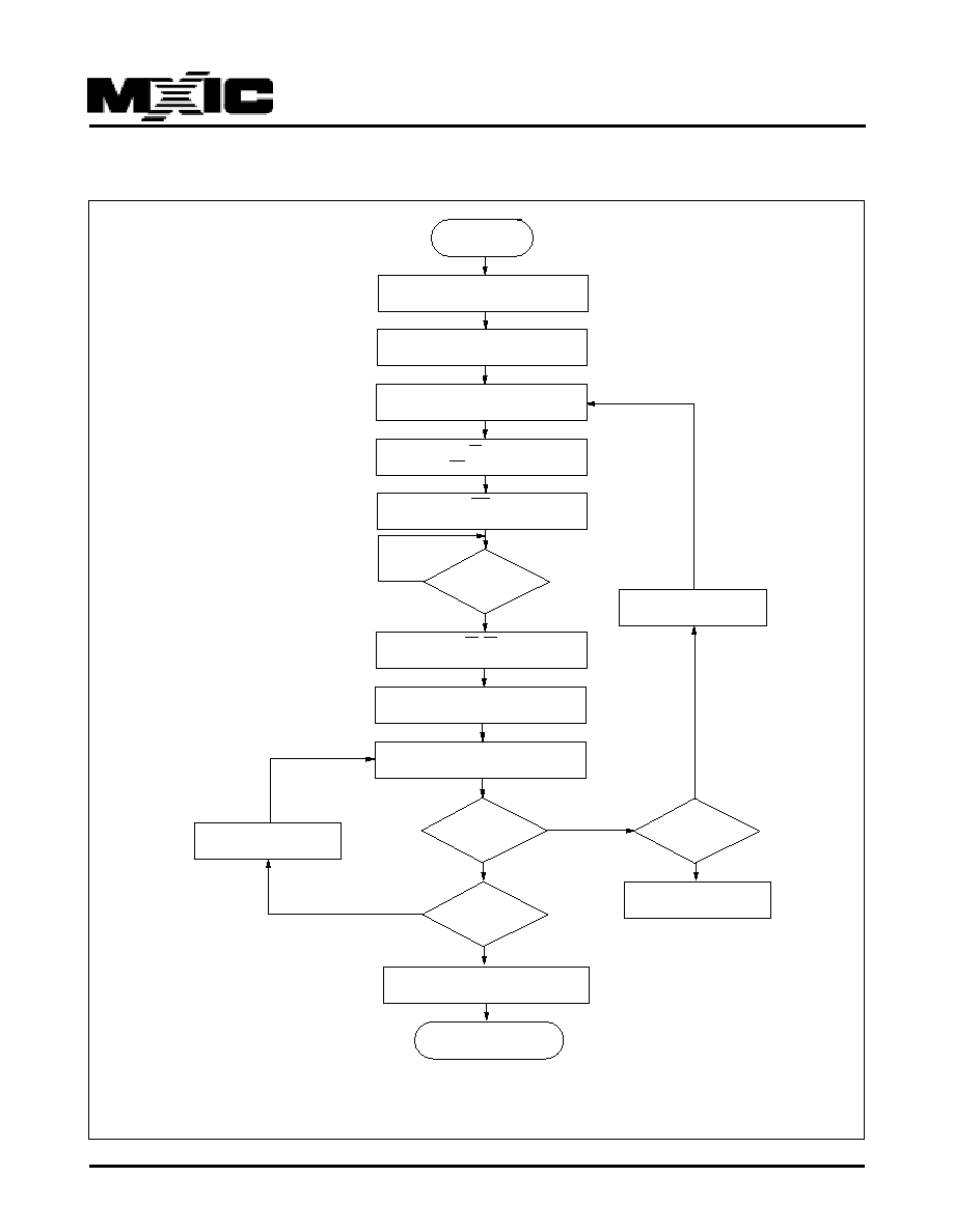
AUTOMATIC CHIP ERASE ALGORITHM FLOWCHART
START
Write Data AAH Address 555H
Write Data 55H Address 2AAH
Write Data AAH Address 555H
Write Data 80H Address 555H
YES
NO
Toggle Bit Checking
Q6 not Toggled
Write Data 10H Address 555H
Write Data 55H Address 2AAH
Reset
Auto Chip Erase Exceed
Timing Limit
DATA Polling
Q7 = 1
YES
Q5 = 1
Auto Chip Erase Completed
NO
NO
Invalid
Command
21
P/N:PM0629
REV. 1.0, DEC. 20, 1999
MX29F4000
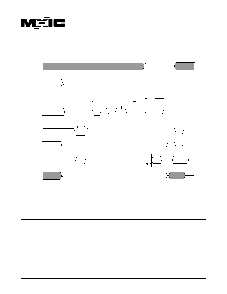
Sector data indicated by A16 to A18 are erased. External
erase verify is not required because data are erased
automatically by internal control circuit. Erasure com-
pletion can be verified by DATA polling and toggle bit
checking after automatic erase starts. Device outputs 0
during erasure and 1 after erasure on Q7.(Q6 is for
toggle bit; see toggle bit, DATA polling, timing waveform)
AUTOMATIC SECTOR ERASE TIMING WAVEFORM
AUTOMATIC SECTOR ERASE TIMING WAVEFORM
tAH
Sector
Address0
555H
2AAH
2AAH
555H
555H
Sector
Address1
Sector
Addressn
Vcc 5V
CE
OE
Q0,Q1,
Q4(Note 1)
WE
A16-A18
Q7
A0~A10
Command
In
Command
In
Command
In
Command
In
Command
In
Command
In
Command
In
Command
In
Command
In
Command
In
Command
In
Command
In
Command
In
Command
In
Command #30H
Command #30H
Command #30H
Command #55H
Command #AAH
Command #80H
Command #55H
Command #AAH
(Q0~Q7)
Command
In
Command
In
tDH
tDS
tCEP
tCWC
tAETB
tBAL
DATA polling
tCEPH1
tAS
Notes:
(1). Q6:Toggle bit, Q5:Timing-limit bit, Q3: Time-out bit, Q2: Toggle bit
22
P/N:PM0629
REV. 1.0, DEC. 20, 1999
MX29F4000
AUTOMATIC SECTOR ERASE ALGORITHM FLOWCHART
START
Write Data AAH Address 555H
Write Data 55H Address 2AAH
Write Data AAH Address 555H
Write Data 80H Address 555H
YES
NO
Toggle Bit Checking
Q6 not Toggled
Write Data 30H Sector Address
Write Data 55H Address 2AAH
Reset
Auto Sector Erase Exceed
Timing Limit
DATA Polling
Q7 = 1
Q5 = 1
Auto Sector Erase Completed
Load Other Sector Addrss If Necessary
(Load Other Sector Address)
YES
NO
Last Sector
to Erase
Time-out Bit
Checking Q3=1 ?
Toggle Bit Checking
Q6 Toggled ?
Invalid Command
NO
YES
YES
NO
23
P/N:PM0629
REV. 1.0, DEC. 20, 1999
MX29F4000
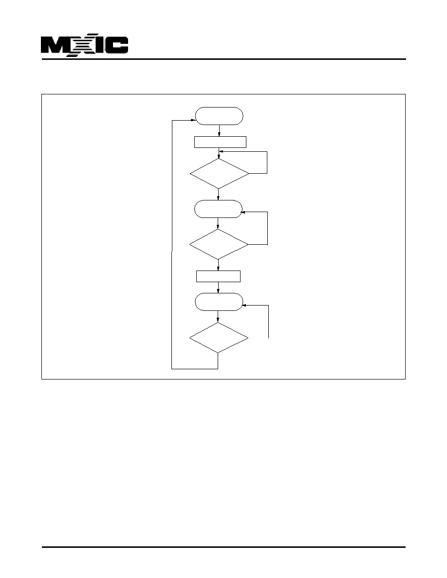
ERASE SUSPEND/ERASE RESUME FLOWCHART
START
Write Data B0H
Toggle Bit checking Q6
not toggled
YES
NO
Write Data 30H
Continue Erase
Reading or
Programming End
Read Array or
Program
Another
Erase Suspend ?
NO
YES
YES
NO
24
P/N:PM0629
REV. 1.0, DEC. 20, 1999
MX29F4000
TIMING WAVEFORM FOR SECTOR PROTECTION FOR SYSTEM WITH 12V
tOE
Data
OE
WE
12V
5V
12V
5V
CE
A9
A1
A6
tOESP
tWPP 1
tVLHT
tVLHT
tVLHT
Verify
01H
F0H
A18-A16
Sector Address
25
P/N:PM0629
REV. 1.0, DEC. 20, 1999
MX29F4000
TIMING WAVEFORM FOR CHIP UNPROTECTION FOR SYSTEM WITH 12V
tOE
Data
OE
WE
12V
5V
12V
5V
CE
A9
A1
tOESP
tWPP 2
tVLHT
tVLHT
tVLHT
Verify
00H
A6
F0H
26
P/N:PM0629
REV. 1.0, DEC. 20, 1999
MX29F4000
SECTOR PROTECTION ALGORITHM FOR SYSTEM WITH 12V
START
Set Up Sector Addr
(A18, A17, A16)
PLSCNT=1
Sector Protection
Complete
Data=01H?
Yes
.
OE=VID,A9=VID,CE=VIL
A6=VIL
Activate WE Pulse
Time Out 10us
Set WE=VIH, CE=OE=VIL
A9 should remain VID
Read from Sector
Addr=SA, A1=1
Protect Another
Sector?
Remove VID from A9
Write Reset Command
Device Failed
PLSCNT=32?
Yes
No
No
27
P/N:PM0629
REV. 1.0, DEC. 20, 1999
MX29F4000
CHIP UNPROTECTION ALGORITHM FOR SYSTEM WITH 12V
START
Protect All Sectors
PLSCNT=1
Chip Unprotect
Complete
Data=00H?
Toggle bit checking
Q6 not Toggled
Yes
Yes
Write "unlock for sector protect/unprotect"
Command (Table 1)
Set OE=A9=VIH
CE=VIL,A6=1
Activate WE Pulse to start
Data do'nt care
Set OE=CE=VIL
A9=VIH,A1=1
Set Up First Sector Addr
All sectors have
been verified?
Write Reset Command
Device Failed
PLSCNT=1000?
No
Increment
PLSCNT
No
Read Data from Device
Yes
Yes
No
No
Increment
Sector Addr
* It is recommended before unprotect whole chip, all sectors should be protected in advance.
28
P/N:PM0629
REV. 1.0, DEC. 20, 1999
MX29F4000
TIMING WAVEFORM FOR SECTOR PROTECTION FOR SYSTEM WITHOUT 12V
tOE
Data
OE
WE
CE
A1
A6
* See the following Note!
Verify
01H
A18-A16
Sector Address
5V
Note1: Must issue "unlock for sector protect/unprotect" command before sector protection
for a system without 12V provided.
Note2: Except F0H
Toggle bit polling
Don't care
(Note 2)
tCEP
F0H

29
P/N:PM0629
REV. 1.0, DEC. 20, 1999
MX29F4000
TIMING WAVEFORM FOR CHIP UNPROTECTION FOR SYSTEM WITHOUT 12V
tOE
Data
WE
CE
A1
Verify
00H
A6
Note1: Must issue "unlock for sector protect/unprotect" command before sector unprotection
for a system without 12V provided.
OE
tCEP
5V
Toggle bit polling
Don't care
(Note 2)
* See the following Note!
F0H
Note2: Except F0H

30
P/N:PM0629
REV. 1.0, DEC. 20, 1999
MX29F4000
SECTOR PROTECTION ALGORITHM FOR SYSTEM WITHOUT 12V
START
Set Up Sector Addr
(A18, A17, A16)
PLSCNT=1
Sector Protection
Complete
Data=01H?
Yes
OE=VIH,A9=VIH
CE=VIL,A6=VIL
Activate WE Pulse to start
Data don't care
Set CE=OE=VIL
A9=VIH
Read from Sector
Addr=SA, A1=1
Protect Another
Sector?
Write Reset Command
Device Failed
PLSCNT=32?
Yes
No
Increment PLSCNT
No
Write "unlock for sector protect/unprotect"
Command(Table1)
Toggle bit checking
Q6 not Toggled
No
.
Yes
31
P/N:PM0629
REV. 1.0, DEC. 20, 1999
MX29F4000
CHIP UNPROTECTION ALGORITHM FOR SYSTEM WITHOUT 12V
START
Protect All Sectors
PLSCNT=1
Chip Unprotect
Complete
Data=00H?
Yes
Set OE=A9=VID
CE=VIL,A6=1
Activate WE Pulse
Time Out 12ms
Set OE=CE=VIL
A9=VID,A1=1
Set Up First Sector Addr
All sectors have
been verified?
Remove VID from A9
Write Reset Command
Device Failed
PLSCNT=1000?
No
Increment
PLSCNT
No
Read Data from Device
Yes
Yes
No
Increment
Sector Addr
* It is recommended before unprotect whole chip, all sectors should be protected in advance.
32
P/N:PM0629
REV. 1.0, DEC. 20, 1999
MX29F4000
ID CODE READ TIMING WAVEFORM
tACC
tCE
tACC
tOE
tOH
tOH
tDF
DATA OUT
C2H
99H
VID
VIH
VIL
ADD
A9
ADD
A2-A8
A10-A18
CE
A1
OE
WE
ADD
A0
DATA OUT
DATA
Q0-Q7
VCC
5V
VIH
VIL
VIH
VIL
VIH
VIL
VIH
VIL
VIH
VIL
VIH
VIL
VIH
VIL

33
P/N:PM0629
REV. 1.0, DEC. 20, 1999
MX29F4000
ORDERING INFORMATION
PLASTIC PACKAGE
PART NO.
ACCESS TIME
OPERATING CURRENT
STANDBY CURRENT
PACKAGE
(ns)
MAX.(mA)
MAX.(uA)
MX29F4000PC-55
55
30
5
32 Pin PDIP
(EPROM pinout)
MX29F4000PC-70
70
30
5
32 Pin PDIP
(EPROM pinout)
MX29F4000PC-90
90
30
5
32 Pin PDIP
(EPROM pinout)
MX29F4000PC-12
120
30
5
32 Pin PDIP
(EPROM pinout)

34
P/N:PM0629
REV. 1.0, DEC. 20, 1999
MX29F4000
MIN.
MAX.
Input Voltage with respect to GND on all pins except I/O pins
-1.0V
13.5V
Input Voltage with respect to GND on all I/O pins
-1.0V
Vcc + 1.0V
Current
-100mA
+100mA
Includes all pins except Vcc. Test conditions: Vcc = 5.0V, one pin at a time.
LIMITS
PARAMETER
MIN.
TYP.(2)
MAX.(3)
UNITS
Sector Erase Time
1.3
10.4
sec
Chip Erase Time
4
32
sec
Byte Programming Time
7
210
us
Chip Programming Time
4
12
sec
Erase/Program Cycles
100,000
Cycles
LATCHUP CHARACTERISTICS
ERASE AND PROGRAMMING PERFORMANCE(1)
Note:
1.Not 100% Tested, Excludes external system level over head.
2.Typical values measured at 25
�
C,5V.
3.Maximunm values measured at 25
�
C,4.5V.
PARAMETER
MIN.
UNIT
Data Retention Time
20
Years
DATA RETENTION

35
P/N:PM0629
REV. 1.0, DEC. 20, 1999
MX29F4000
REVISION HISTORY
Revision
Description
Page
Date
1.0
1.To remove "Advanced Information" datasheet marking and
P1
DEC/20/1999
contain information on products in full production
2.The modification summary of Revision 0.1 & Revision 1.0:
2-1.Program/erase cycle times:10K cycles-->100K cycles
P1,34
2-2.To add data retention 20 years
P1,34
2-3.To modify timing of sector address loading period while
P8
operating multi-sector erase from 80us to 30us
2-4.To modify tBAL from 80us to 100us
P15
2-5.To remove A9 from "timing waveform for sector protection for
P28
system without 12V"
To remove A9 from "timing waveform for chip unprotection for P29
system without 12V"

M
ACRONIX
I
NTERNATIONAL
C
O.,
L
TD.
HEADQUARTERS:
TEL:+886-3-578-8888
FAX:+886-3-578-8887
EUROPE OFFICE:
TEL:+32-2-456-8020
FAX:+32-2-456-8021
JAPAN OFFICE:
TEL:+81-44-246-9100
FAX:+81-44-246-9105
SINGAPORE OFFICE:
TEL:+65-747-2309
FAX:+65-748-4090
TAIPEI OFFICE:
TEL:+886-3-509-3300
FAX:+886-3-509-2200
M
ACRONIX
A
MERICA,
I
NC.
TEL:+1-408-453-8088
FAX:+1-408-453-8488
CHICAGO OFFICE:
TEL:+1-847-963-1900
FAX:+1-847-963-1909
http : //www.macronix.com
MACRONIX INTERNATIONAL CO., LTD. reserves the rignt to change product and specifications without notice.
36
MX29F4000