
1
P/N:PM1008
REV. 1.1, MAY 28, 2004
MX29LV320AT/B
32M-BIT [4M x 8 / 2M x 16] SINGLE VOLTAGE
3V ONLY FLASH MEMORY
FEATURES
GENERAL FEATURES
∑ 4,194,304 x 8 / 2,097,152 x 16 switchable
∑ Sector Structure
- 8K-Byte x 8 and 64K-Byte x 63
∑ Extra 64K-Byte sector for security
- Features factory locked and identifiable, and cus-
tomer lockable
∑ Twenty-Four Sector Groups
- Provides sector group protect function to prevent pro-
gram or erase operation in the protected sector group
- Provides chip unprotect function to allow code chang-
ing
- Provides temporary sector group unprotect function
for code changing in previously protected sector groups
∑ Single Power Supply Operation
- 2.7 to 3.6 volt for read, erase, and program opera-
tions
∑ Latch-up protected to 250mA from -1V to Vcc + 1V
∑ Low Vcc write inhibit is equal to or less than 1.4V
∑ Compatible with JEDEC standard
- Pinout and software compatible to single power sup-
ply Flash
∑ 2nd generation of 3V/32M Flash product
- Fully compatible with MX29LV320T/B device
PERFORMANCE
∑ High Performance
- Fast access time: 70/90ns
- Fast program time: 7us/word typical utilizing acceler-
ate function
- Fast erase time: 0.9s/sector, 35s/chip (typical)
∑ Low Power Consumption
- Low active read current: 10mA (typical) at 5MHz
- Low standby current: 200nA (typical)
∑ Minimum 100,000 erase/program cycle
∑ 10 years data retention
SOFTWARE FEATURES
∑ Erase Suspend/ Erase Resume
- Suspends sector erase operation to read data from
or program data to another sector which is not being
erased
∑ Status Reply
- Data polling & Toggle bits provide detection of pro-
gram and erase operation completion
∑ Support Common Flash Interface (CFI)
HARDWARE FEATURES
∑ Ready/Busy (RY/BY) Output
- Provides a hardware method of detecting program
and erase operation completion
∑ Hardware Reset (RESET) Input
- Provides a hardware method to reset the internal state
machine to read mode
∑ WP/ACC input pin
- Provides accelerated program capability
PACKAGE
∑ 48-Pin TSOP
∑ 48-Ball CSP
GENERAL DESCRIPTION
The MX29LV320AT/B is a 32-mega bit Flash memory
organized as 4M bytes of 8 bits and 2M words of 16 bits.
MXIC's Flash memories offer the most cost-effective and
reliable read/write non-volatile random access memory.
The MX29LV320AT/B is packaged in 48-pin TSOP and
48-ball CSP. It is designed to be reprogrammed and
erased in system or in standard EPROM programmers.
The standard MX29LV320AT/B offers access time as
fast as 70ns, allowing operation of high-speed micropro-
cessors without wait states. To eliminate bus conten-
tion, the MX29LV320AT/B has separate chip enable (CE)
and output enable (OE) controls.
MXIC's Flash memories augment EPROM functionality
with in-circuit electrical erasure and programming. The
MX29LV320AT/B uses a command register to manage
this functionality.
MXIC Flash technology reliably stores memory
contents even after 100,000 erase and program
cycles. The MXIC cell is designed to optimize the
erase and program mechanisms. In addition, the
combination of advanced tunnel oxide processing
and low internal electric fields for erase and
programming operations produces reliable cycling.

2
P/N:PM1008
REV. 1.1, MAY 28, 2004
MX29LV320AT/B
AUTOMATIC PROGRAMMING
The MX29LV320AT/B is byte/word programmable using
the Automatic Programming algorithm. The Automatic
Programming algorithm makes the external system do
not need to have time out sequence nor to verify the
data programmed. The typical chip programming time at
room temperature of the MX29LV320AT/B is less than
36 seconds.
AUTOMATIC PROGRAMMING ALGORITHM
MXIC's Automatic Programming algorithm require the user
to only write program set-up commands (including 2 un-
lock write cycle and A0H) and a program command (pro-
gram data and address). The device automatically times
the programming pulse width, provides the program veri-
fication, and counts the number of sequences. A status
bit similar to DATA polling and a status bit toggling be-
tween consecutive read cycles, provide feedback to the
user as to the status of the programming operation.
AUTOMATIC CHIP ERASE
The entire chip is bulk erased using 50 ms erase pulses
according to MXIC's Automatic Chip Erase algorithm.
Typical erasure at room temperature is accomplished in
less than 35 seconds. The Automatic Erase algorithm
automatically programs the entire array prior to electri-
cal erase. The timing and verification of electrical erase
are controlled internally within the device.
AUTOMATIC SECTOR ERASE
The MX29LV320AT/B is sector(s) erasable using
MXIC's Auto Sector Erase algorithm. Sector erase
modes allow sectors of the array to be erased in one
erase cycle. The Automatic Sector Erase algorithm
automatically programs the specified sector(s) prior to
electrical erase. The timing and verification of
electrical erase are controlled internally within the
device.
AUTOMATIC ERASE ALGORITHM
MXIC's Automatic Erase algorithm requires the user to
write commands to the command register using stand-
ard microprocessor write timings. The device will auto-
matically pre-program and verify the entire array. Then
the device automatically times the erase pulse width,
provides the erase verification, and counts the number
of sequences. A status bit toggling between consecu-
tive read cycles provides feedback to the user as to the
status of the programming operation.
Register contents serve as inputs to an internal state-
machine which controls the erase and programming cir-
cuitry. During write cycles, the command register inter-
nally latches address and data needed for the program-
ming and erase operations. During a system write cycle,
addresses are latched on the falling edge, and data are
latched on the rising edge of WE .
MXIC's Flash technology combines years of EPROM
experience to produce the highest levels of quality, relia-
bility, and cost effectiveness. The MX29LV320AT/B elec-
trically erases all bits simultaneously using Fowler-Nord-
heim tunneling. The bytes/words are programmed by
using the EPROM programming mechanism of hot elec-
tron injection.
During a program cycle, the state-machine will control
the program sequences and command register will not
respond to any command set. During a Sector Erase
cycle, the command register will only respond to Erase
Suspend command. After Erase Suspend is completed,
the device stays in read mode. After the state machine
has completed its task, it will allow the command regis-
ter to respond to its full command set.
The MX29LV320AT/B uses a 2.7V to 3.6V VCC
supply to perform the High Reliability Erase and
auto Program/Erase algorithms.
The highest degree of latch-up protection is
achieved with MXIC's proprietary non-epi process.
Latch-up protection is proved for stresses up to 100
milliamperes on address and data pin from -1V to
VCC + 1V.

3
P/N:PM1008
REV. 1.1, MAY 28, 2004
MX29LV320AT/B
PIN CONFIGURATION
48 TSOP
SYMBOL
PIN NAME
A0~A20
Address Input
Q0~Q14
15 Data Inputs/Outputs
Q15/A-1
Q15(Data Input/Output, word mode)
A-1(LSB Address Input, byte mode)
CE
Chip Enable Input
WE
Write Enable Input
OE
Output Enable Input
BYTE
Word/Byte Selection Input
RESET
Hardware Reset Pin, Active Low
RY/BY
Read/Busy Output
VCC
3.0 volt-only single power supply
WP/ACC
Hardware Write Protect/Acceleration
Pin
GND
Device Ground
NC
Pin Not Connected Internally
PIN DESCRIPTION
LOGIC SYMBOL
48-Ball CSP 6mm x 8mm (Ball Pitch = 0.8 mm), Top View, Balls Facing Down
A
B
C
D
E
F
G
H
6
A13
A12
A14
A15
A16
BYTE
Q15/A-1 GND
5
A9
A8
A10
A11
Q7
Q14
Q13
Q6
4
WE
RESET
NC
A19
Q5
Q12
Vcc
Q4
3
RY/BY WP/ACC
A18
A20
Q2
Q10
Q11
Q3
2
A7
A17
A6
A5
Q0
Q8
Q9
Q1
1
A3
A4
A2
A1
A0
CE
OE
GND
16 or 8
Q0-Q15
(A-1)
RY/BY
A0-A20
WP/ACC
CE
OE
WE
RESET
BYTE
21
A15
A14
A13
A12
A11
A10
A9
A8
A19
A20
WE
RESET
NC
WP/ACC
RY/BY
A18
A17
A7
A6
A5
A4
A3
A2
A1
1
2
3
4
5
6
7
8
9
10
11
12
13
14
15
16
17
18
19
20
21
22
23
24
A16
BYTE
GND
Q15/A-1
Q7
Q14
Q6
Q13
Q5
Q12
Q4
VCC
Q11
Q3
Q10
Q2
Q9
Q1
Q8
Q0
OE
GND
CE
A0
48
47
46
45
44
43
42
41
40
39
38
37
36
35
34
33
32
31
30
29
28
27
26
25
MX29LV320AT/B

4
P/N:PM1008
REV. 1.1, MAY 28, 2004
MX29LV320AT/B
BLOCK DIAGRAM
CONTROL
INPUT
LOGIC
PROGRAM/ERASE
HIGH VOLTAGE
WRITE
STATE
MACHINE
(WSM)
STATE
REGISTER
MX29LV320AT/B
FLASH
ARRAY
X-DECODER
ADDRESS
LATCH
AND
BUFFER
Y-PASS GATE
Y
-DECODER
ARRAY
SOURCE
HV
COMMAND
DATA
DECODER
COMMAND
DATA LATCH
I/O BUFFER
PGM
DATA
HV
PROGRAM
DATA LATCH
SENSE
AMPLIFIER
Q0-Q15/A-1
A0-A20
CE
OE
WE
RESET
BYTE

5
P/N:PM1008
REV. 1.1, MAY 28, 2004
MX29LV320AT/B
Sector
Sector
Sector Address
Sector Size
(x8)
(x16)
Group
A20-A12
(Kbytes/Kwords)
Address Range
Address Range
1
SA0
000000xxx
64/32
000000h-00FFFFh
000000h-07FFFh
1
SA1
000001xxx
64/32
010000h-01FFFFh
008000h-0FFFFh
1
SA2
000010xxx
64/32
020000h-02FFFFh
010000h-17FFFh
1
SA3
000011xxx
64/32
030000h-03FFFFh
018000h-01FFFFh
2
SA4
000100xxx
64/32
040000h-04FFFFh
020000h-027FFFh
2
SA5
000101xxx
64/32
050000h-05FFFFh
028000h-02FFFFh
2
SA6
000110xxx
64/32
060000h-06FFFFh
030000h-037FFFh
2
SA7
000111xxx
64/32
070000h-07FFFFh
038000h-03FFFFh
3
SA8
001000xxx
64/32
080000h-08FFFFh
040000h-047FFFh
3
SA9
001001xxx
64/32
090000h-09FFFFh
048000h-04FFFFh
3
SA10
001010xxx
64/32
0A0000h-0AFFFFh
050000h-057FFFh
3
SA11
001011xxx
64/32
0B0000h-0BFFFFh
058000h-05FFFFh
4
SA12
001100xxx
64/32
0C0000h-0CFFFFh
060000h-067FFFh
4
SA13
001101xxx
64/32
0D0000h-0DFFFFh
068000h-06FFFFh
4
SA14
001110xxx
64/32
0E0000h-0EFFFFh
070000h-077FFFh
4
SA15
001111xxx
64/32
0F0000h-0FFFFFh
078000h-07FFFFh
5
SA16
010000xxx
64/32
100000h-10FFFFh
080000h-087FFFh
5
SA17
010001xxx
64/32
110000h-11FFFFh
088000h-08FFFFh
5
SA18
010010xxx
64/32
120000h-12FFFFh
090000h-097FFFh
5
SA19
010011xxx
64/32
130000h-13FFFFh
098000h-09FFFFh
6
SA20
010100xxx
64/32
140000h-14FFFFh
0A0000h-0A7FFFh
6
SA21
010101xxx
64/32
150000h-15FFFFh
0A8000h-0AFFFFh
6
SA22
010110xxx
64/32
160000h-16FFFFh
0B0000h-0B7FFFh
6
SA23
010111xxx
64/32
170000h-17FFFFh
0B8000h-0BFFFFh
7
SA24
011000xxx
64/32
180000h-18FFFFh
0C0000h-0C7FFFh
7
SA25
011001xxx
64/32
190000h-19FFFFh
0C8000h-0CFFFFh
7
SA26
011010xxx
64/32
1A0000h-1AFFFFh
0D0000h-0D7FFFh
7
SA27
011011xxx
64/32
1B0000h-1BFFFFh
0D8000h-0DFFFFh
8
SA28
011100xxx
64/32
1C0000h-1CFFFFh
0E0000h-0E7FFFh
8
SA29
011101xxx
64/32
1D0000h-1DFFFFh
0E8000h-0EFFFFh
8
SA30
011110xxx
64/32
1E0000h-1EFFFFh
0F0000h-0F7FFFh
8
SA31
011111xxx
64/32
1F0000h-1FFFFFh
0F8000h-0FFFFFh
9
SA32
100000xxx
64/32
200000h-20FFFFh
100000h-107FFFh
9
SA33
100001xxx
64/32
210000h-21FFFFh
108000h-10FFFFh
9
SA34
100010xxx
64/32
220000h-22FFFFh
110000h-117FFFh
9
SA35
100011xxx
64/32
230000h-23FFFFh
118000h-11FFFFh
10
SA36
100100xxx
64/32
240000h-24FFFFh
120000h-127FFFh
10
SA37
100101xxx
64/32
250000h-25FFFFh
128000h-12FFFFh
10
SA38
100110xxx
64/32
260000h-26FFFFh
130000h-137FFFh
10
SA39
100111xxx
64/32
270000h-27FFFFh
138000h-13FFFFh
Table 1.a: MX29LV320AT SECTOR GROUP ARCHITECTURE

6
P/N:PM1008
REV. 1.1, MAY 28, 2004
MX29LV320AT/B
Sector
Sector
Sector Address
Sector Size
(x8)
(x16)
Group
A20-A12
(Kbytes/Kwords)
Address Range
Address Range
11
SA40
101000xxx
64/32
280000h-28FFFFh
140000h-147FFFh
11
SA41
101001xxx
64/32
290000h-29FFFFh
148000h-14FFFFh
11
SA42
101010xxx
64/32
2A0000h-2AFFFFh
150000h-157FFFh
11
SA43
101011xxx
64/32
2B0000h-2BFFFFh
158000h-15FFFFh
12
SA44
101100xxx
64/32
2C0000h-2CFFFFh
160000h-147FFFh
12
SA45
101101xxx
64/32
2D0000h-2DFFFFh
168000h-14FFFFh
12
SA46
101110xxx
64/32
2E0000h-2EFFFFh
170000h-177FFFh
12
SA47
101111xxx
64/32
2F0000h-2FFFFFh
178000h-17FFFFh
13
SA48
110000xxx
64/32
300000h-30FFFFh
180000h-187FFFh
13
SA49
110001xxx
64/32
310000h-31FFFFh
188000h-18FFFFh
13
SA50
110010xxx
64/32
320000h-32FFFFh
190000h-197FFFh
13
SA51
110011xxx
64/32
330000h-33FFFFh
198000h-19FFFFh
14
SA52
110100xxx
64/32
340000h-34FFFFh
1A0000h-1A7FFFh
14
SA53
110101xxx
64/32
350000h-35FFFFh
1A8000h-1AFFFFh
14
SA54
110110xxx
64/32
360000h-36FFFFh
1B0000h-1B7FFFh
14
SA55
110111xxx
64/32
370000h-37FFFFh
1B8000h-1BFFFFh
15
SA56
111000xxx
64/32
380000h-38FFFFh
1C0000h-1C7FFFh
15
SA57
111001xxx
64/32
390000h-39FFFFh
1C8000h-1CFFFFh
15
SA58
111010xxx
64/32
3A0000h-3AFFFFh
1D0000h-1D7FFFh
15
SA59
111011xxx
64/32
3B0000h-3BFFFFh
1D8000h-1DFFFFh
16
SA60
111100xxx
64/32
3C0000h-3CFFFFh
1E0000h-1E7FFFh
16
SA61
111101xxx
64/32
3D0000h-3DFFFFh
1E8000h-1EFFFFh
16
SA62
111110xxx
64/32
3E0000h-3EFFFFh
1F0000h-1F7FFFh
17
SA63
111111000
8/4
3F0000h-3F1FFFh
1F8000h-1F8FFFh
18
SA64
111111001
8/4
3F2000h-3F3FFFh
1F9000h-1F9FFFh
19
SA65
111111010
8/4
3F4000h-3F5FFFh
1FA000h-1FAFFFh
20
SA66
111111011
8/4
3F6000h-3F7FFFh
1FB000h-1FBFFFh
21
SA67
111111100
8/4
3F8000h-3F9FFFh
1FC000h-1FCFFFh
22
SA68
111111101
8/4
3FA000h-3FBFFFh
1FD000h-1FDFFFh
23
SA69
111111110
8/4
3FC000h-3FDFFFh
1FE000h-1FEFFFh
24
SA70
111111111
8/4
3FE000h-3FFFFFh
1FF000h-1FFFFFh
Top Boot Security Sector Addresses
Sector Address
Sector Size
(x8)
(x16)
A20~A12
(Kbytes/Kwords)
Address Range
Address Range
111111xxx
64/32
3F0000h-3FFFFFh
1F8000h-1FFFFFh
Note:The address range is A20:A-1 in byte mode (BYTE=VIL) or A20:A0 in word mode (BYTE=VIH)

7
P/N:PM1008
REV. 1.1, MAY 28, 2004
MX29LV320AT/B
Sector
Sector
Sector Address
Sector Size
(x8)
(x16)
Group
A20-A12
(Kbytes/Kwords)
Address Range
Address Range
1
SA0
000000000
8/4
000000h-001FFFh
000000h-000FFFh
2
SA1
000000001
8/4
002000h-003FFFh
001000h-001FFFh
3
SA2
000000010
8/4
004000h-005FFFh
002000h-002FFFh
4
SA3
000000011
8/4
006000h-007FFFh
003000h-003FFFh
5
SA4
000000100
8/4
008000h-009FFFh
004000h-004FFFh
6
SA5
000000101
8/4
00A000h-00BFFFh
005000h-005FFFh
7
SA6
000000110
8/4
00C000h-00DFFFh
006000h-006FFFh
8
SA7
000000111
8/4
00E000h-00FFFFh
007000h-007FFFh
9
SA8
000001xxx
64/32
010000h-01FFFFh
008000h-00FFFFh
9
SA9
000010xxx
64/32
020000h-02FFFFh
010000h-017FFFh
9
SA10
000011xxx
64/32
030000h-03FFFFh
018000h-01FFFFh
10
SA11
000100xxx
64/32
040000h-04FFFFh
020000h-027FFFh
10
SA12
000101xxx
64/32
050000h-05FFFFh
028000h-02FFFFh
10
SA13
000110xxx
64/32
060000h-06FFFFh
030000h-037FFFh
10
SA14
000111xxx
64/32
070000h-07FFFFh
038000h-03FFFFh
11
SA15
001000xxx
64/32
080000h-08FFFFh
040000h-047FFFh
11
SA16
001001xxx
64/32
090000h-09FFFFh
048000h-04FFFFh
11
SA17
001010xxx
64/32
0A0000h-0AFFFFh
050000h-057FFFh
11
SA18
001011xxx
64/32
0B0000h-0BFFFFh
058000h-05FFFFh
12
SA19
001100xxx
64/32
0C0000h-0CFFFFh
060000h-067FFFh
12
SA20
001101xxx
64/32
0D0000h-0DFFFFh
068000h-06FFFFh
12
SA21
001110xxx
64/32
0E0000h-0EFFFFh
070000h-077FFFh
12
SA22
001111xxx
64/32
0F0000h-0FFFFFh
078000h-07FFFFh
13
SA23
010000xxx
64/32
100000h-10FFFFh
080000h-087FFFh
13
SA24
010001xxx
64/32
110000h-11FFFFh
088000h-08FFFFh
13
SA25
010010xxx
64/32
120000h-12FFFFh
090000h-097FFFh
13
SA26
010011xxx
64/32
130000h-13FFFFh
098000h-09FFFFh
14
SA27
010100xxx
64/32
140000h-14FFFFh
0A0000h-0A7FFFh
14
SA28
010101xxx
64/32
150000h-15FFFFh
0A8000h-0AFFFFh
14
SA29
010110xxx
64/32
160000h-16FFFFh
0B0000h-0B7FFFh
14
SA30
010111xxx
64/32
170000h-17FFFFh
0B8000h-0BFFFFh
15
SA31
011000xxx
64/32
180000h-18FFFFh
0C0000h-0C7FFFh
15
SA32
011001xxx
64/32
190000h-19FFFFh
0C8000h-0CFFFFh
15
SA33
011010xxx
64/32
1A0000h-1AFFFFh
0D0000h-0D7FFFh
15
SA34
011011xxx
64/32
1B0000h-1BFFFFh
0D8000h-0DFFFFh
16
SA35
011100xxx
64/32
1C0000h-1CFFFFh
0E0000h-0E7FFFh
16
SA36
011101xxx
64/32
1D0000h-1DFFFFh
0E8000h-0EFFFFh
16
SA37
011110xxx
64/32
1E0000h-1EFFFFh
0F0000h-0F7FFFh
16
SA38
011111xxx
64/32
1F0000h-1FFFFFh
0F8000h-0FFFFFh
Table 1.b: MX29LV320AB SECTOR GROUP ARCHITECTURE

8
P/N:PM1008
REV. 1.1, MAY 28, 2004
MX29LV320AT/B
Sector
Sector
Sector Address
Sector Size
(x8)
(x16)
Group
A20-A12
(Kbytes/Kwords)
Address Range
Address Range
17
SA39
100000xxx
64/32
200000h-20FFFFh
100000h-107FFFh
17
SA40
100001xxx
64/32
210000h-21FFFFh
108000h-10FFFFh
17
SA41
100010xxx
64/32
220000h-22FFFFh
110000h-117FFFh
17
SA42
100011xxx
64/32
230000h-23FFFFh
118000h-11FFFFh
18
SA43
100100xxx
64/32
240000h-24FFFFh
120000h-127FFFh
18
SA44
100101xxx
64/32
250000h-25FFFFh
128000h-12FFFFh
18
SA45
100110xxx
64/32
260000h-26FFFFh
130000h-137FFFh
18
SA46
100111xxx
64/32
270000h-27FFFFh
138000h-13FFFFh
19
SA47
101000xxx
64/32
280000h-28FFFFh
140000h-147FFFh
19
SA48
101001xxx
64/32
290000h-29FFFFh
148000h-14FFFFh
19
SA49
101010xxx
64/32
2A0000h-2AFFFFh
150000h-157FFFh
19
SA50
101011xxx
64/32
2B0000h-2BFFFFh
158000h-15FFFFh
20
SA51
101100xxx
64/32
2C0000h-2CFFFFh
160000h-167FFFh
20
SA52
101101xxx
64/32
2D0000h-2DFFFFh
168000h-16FFFFh
20
SA53
101110xxx
64/32
2E0000h-2EFFFFh
170000h-177FFFh
20
SA54
101111xxx
64/32
2F0000h-2FFFFFh
178000h-17FFFFh
21
SA55
110000xxx
64/32
300000h-30FFFFh
180000h-187FFFh
21
SA56
110001xxx
64/32
310000h-31FFFFh
188000h-18FFFFh
21
SA57
110010xxx
64/32
320000h-32FFFFh
190000h-197FFFh
21
SA58
110011xxx
64/32
330000h-33FFFFh
198000h-19FFFFh
22
SA59
110100xxx
64/32
340000h-34FFFFh
1A0000h-1A7FFFh
22
SA60
110101xxx
64/32
350000h-35FFFFh
1A8000h-1AFFFFh
22
SA61
110110xxx
64/32
360000h-36FFFFh
1B0000h-1B7FFFh
22
SA62
110111xxx
64/32
370000h-37FFFFh
1B8000h-1BFFFFh
23
SA63
111000xxx
64/32
380000h-38FFFFh
1C0000h-1C7FFFh
23
SA64
111001xxx
64/32
390000h-39FFFFh
1C8000h-1CFFFFh
23
SA65
111010xxx
64/32
3A0000h-3AFFFFh
1D0000h-1D7FFFh
23
SA66
111011xxx
64/32
3B0000h-3BFFFFh
1D8000h-1DFFFFh
24
SA67
111100xxx
64/32
3C0000h-3CFFFFh
1E0000h-1E7FFFh
24
SA68
111101xxx
64/32
3D0000h-3DFFFFh
1E8000h-1EFFFFh
24
SA69
111110xxx
64/32
3E0000h-3EFFFFh
1F0000h-1F7FFFh
24
SA70
111111xxx
64/32
3F0000h-3FFFFFh
1F8000h-1FFFFFh
Bottom Boot Security Sector Addresses
Sector Address
Sector Size
(x8)
(x16)
A20~A12
(Kbytes/Kwords)
Address Range
Address Range
111111xxx
64/32
000000h-00FFFFh
00000h-07FFFh
Note:The address range is A20:A-1 in byte mode (BYTE=VIL) or A20:A0 in word mode (BYTE=VIH)

9
P/N:PM1008
REV. 1.1, MAY 28, 2004
MX29LV320AT/B
Operation
CE
OE
WE RESET WP/ACC
Addresses
Q0~Q7
Q8 ~ Q15
(Note 2)
Byte=VIH
Byte=VIL
Read
L
L
H
H
L/H
A
IN
D
OUT
D
OUT
Q8-A14
=High-Z
Write (Note 1)
L
H
L
H
Note 3
A
IN
D
IN
D
IN
Q15=A-1
Accelerate
L
H
L
H
V
HH
A
IN
D
IN
D
IN
Program
Standby
VCC
±
X
X
VCC
±
H
X
High-Z
High-Z
High-Z
0.3V
0.3V
Output Disable
L
H
H
H
L/H
X
High-Z
High-Z
High-Z
Reset
X
X
X
L
L/H
X
High-Z
High-Z
High-Z
Sector Group
L
H
L
V
ID
L/H
Sector Addresses, D
IN
, D
OUT
X
X
Protect (Note 2)
A6=L, A1=H, A0=L
Chip Unprotect
L
H
L
V
ID
Note 3
Sector Addresses, D
IN
, D
OUT
X
X
(Note 2)
A6=H, A1=H, A0=L
Temporary Sector
X
X
X
V
ID
Note 3
A
IN
D
IN
D
IN
High-Z
Group Unprotect
Legend:
L=Logic LOW=V
IL
, H=Logic High=V
IH
, V
ID
=12.0
±
0.5V, V
HH
=11.5-12.5V, X=Don't Care, A
IN
=Address IN, D
IN
=Data IN,
D
OUT
=Data OUT
Notes:
1. When the WP/ACC pin is at V
HH
, the device enters the accelerated program mode. See "Accelerated Program
Operations" for more information.
2.The sector group protect and chip unprotect functions may also be implemented via programming equipment. See
the "Sector Group Protection and Chip Unprotection" section.
3.If WP/ACC=V
IL
, the two outermost boot sectors remain protected. If WP/ACC=V
IH
, the two outermost boot sector
protection depends on whether they were last protected or unprotected using the method described in "Sector/
Sector Block Protection and Unprotection". If WP/ACC=V
HH
, all sectors will be unprotected.
4.DIN or Dout as required by command sequence, data polling, or sector protection algorithm.
5.Address are A20:A0 in word mode (BYTE=V
IH
), A20:A-1 in byte mode (BYTE=V
IL
).
Table 2. BUS OPERATION--1

10
P/N:PM1008
REV. 1.1, MAY 28, 2004
MX29LV320AT/B
A20
A11
A9
A8
A6
A5
Operation
CE
OE
WE
to
to
to
to
A1
A0
Q0-Q7
Q8-Q15
A12
A10
A7
A2
Read Silicon ID
L
L
H
X
X
V
ID
X
L
X
L
L
C2H
X
Manufacturer Code
Read Silicon ID
L
L
H
X
X
V
ID
X
L
X
L
H
A7H
22h(word)
MX29LV320AT
X (byte)
Read Silicon ID
L
L
H
X
X
V
ID
X
L
X
L
H
A8H
22h(word)
MX29LV320AB
X (byte)
Sector Protect
L
L
H
SA
X
V
ID
X
L
X
H
L
01h(1),
X
Verification
or 00h
Security Sector
L
L
H
X
X
V
ID
X
L
X
H
H
99h(2),
X
Indicater
or 19h
Bit (Q7)
BUS OPERATION--2
Notes:
1.Code=00h means unprotected, or code=01h protected.
2.Code=99 means factory locked, or code=19h not factory locked.

11
P/N:PM1008
REV. 1.1, MAY 28, 2004
MX29LV320AT/B
REQUIREMENTS FOR READING ARRAY
DATA
To read array data from the outputs, the system must
drive the CE and OE pins to VIL. CE is the power control
and selects the device. OE is the output control and gates
array data to the output pins. WE should remain at VIH.
The internal state machine is set for reading array data
upon device power-up, or after a hardware reset. This
ensures that no spurious alteration of the memory content
occurs during the power transition. No command is
necessary in this mode to obtain array data. Standard
microprocessor read cycles that assert valid address on
the device address inputs produce valid data on the device
data outputs. The device remains enabled for read access
until the command register contents are altered.
WRITE COMMANDS/COMMAND SEQUENCES
To program data to the device or erase sectors of memory
, the system must drive WE and CE to VIL, and OE to
VIH.
An erase operation can erase one sector, multiple sectors
, or the entire device. Table 1 indicates the address space
that each sector occupies. A "sector address" consists
of the address bits required to uniquely select a sector.
Writing specific address and data commands or
sequences into the command register initiates device
operations. Table 3 defines the valid register command
sequences. Writing incorrect address and data values or
writing them in the improper sequence resets the device
to reading array data. Section has details on erasing a
sector or the entire chip, or suspending/resuming the erase
operation.
After the system writes the Automatic Select command
sequence, the device enters the Automatic Select mode.
The system can then read Automatic Select codes from
the internal register (which is separate from the memory
array) on Q7-Q0. Standard read cycle timings apply in
this mode. Refer to the Automatic Select Mode and
Automatic Select Command Sequence section for more
information.
ICC2 in the DC Characteristics table represents the active
current specification for the write mode. The "AC
Characteristics" section contains timing specification
table and timing diagrams for write operations.
ACCELERATED PROGRAM OPERATION
The device offers accelerated program operations through
the WP/ACC function. If the system asserts V
HH
on ACC
pin, the device will provide the fast programming time to
user. This function is primarily intended to allow faster
manufacturing throughput during production. Removing
V
HH
from the WP/ACC pin returns the device to normal
operation. Note that the WP/ACC pin must not be at V
HH
for operations other than accelerated programming, or
device damage may result.
STANDBY MODE
MX29LV320AT/B can be set into Standby mode with two
different approaches. One is using both CE and RESET
pins and the other one is using RESET pin only.
When using both pins of CE and RESET, a CMOS
Standby mode is achieved with both pins held at Vcc ±
0.3V. Under this condition, the current consumed is less
than 0.2uA (typ.). If both of the CE and RESET are held
at VIH, but not within the range of VCC ±
0.3V, the device
will still be in the standby mode, but the standby current
will be larger. During Auto Algorithm operation, Vcc ac-
tive current (ICC2) is required even CE = "H" until the
operation is completed. The device can be read with stan-
dard access time (tCE) from either of these standby
modes.
When using only RESET, a CMOS standby mode is
achieved with RESET input held at Vss
±
0.3V, Under
this condition the current is consumed less than 1uA
(typ.). Once the RESET pin is taken high, the device is
back to active without recovery delay.
In the standby mode the outputs are in the high imped-
ance state, independent of the OE input.
MX29LV320AT/B is capable to provide the Automatic
Standby Mode to restrain power consumption during read-
out of data. This mode can be used effectively with an
application requested low power consumption such as
handy terminals.
To active this mode, MX29LV320AT/B automatically
switch themselves to low power mode when
MX29LV320AT/B addresses remain stable during access
time of tACC+30ns. It is not necessary to control CE,
WE, and OE on the mode. Under the mode, the current
consumed is typically 0.2uA (CMOS level).

12
P/N:PM1008
REV. 1.1, MAY 28, 2004
MX29LV320AT/B
OUTPUT DISABLE
With the OE input at a logic high level (VIH), output from
the devices are disabled. This will cause the output pins
to be in a high impedance state.
RESET OPERATION
The RESET pin provides a hardware method of resetting
the device to reading array data. When the RESET pin is
driven low for at least a period of tRP, the device
immediately terminates any operation in progress,
tristates all output pins, and ignores all read/write
commands for the duration of the RESET pulse. The
device also resets the internal state machine to reading
array data. The operation that was interrupted should be
reinitiated once the device is ready to accept another
command sequence, to ensure data integrity
Current is reduced for the duration of the RESET pulse.
When RESET is held at VSS
±
0.3V, the device draws
CMOS standby current (ICC4). If RESET is held at VIL
but not within VSS
±
0.3V, the standby current will be
greater.
The RESET pin may be tied to system reset circuitry. A
system reset would that also reset the Flash memory,
enabling the system to read the boot-up firm-ware from
the Flash memory.
If RESET is asserted during a program or erase
operation, the RY/BY pin remains a "0" (busy) until the
internal reset operation is complete, which requires a time
of tREADY (during Embedded Algorithms). The system
can thus monitor RY/BY to determine whether the reset
operation is complete. If RESET is asserted when a
program or erase operation is not executing (RY/BY pin
is "1"), the reset operation is completed within a time of
tREADY (not during Embedded Algorithms). The system
can read data tRH after the RESET pin returns to VIH.
Refer to the AC Characteristics tables for RESET
parameters and to Figure 14 for the timing diagram.
SECTOR GROUP PROTECT OPERATION
The MX29LV320AT/B features hardware sector group
protection. This feature will disable both program and
erase operations for these sector group protected. Sec-
tor protection can be implemented via two methods.
The primary method requires VID on the RESET only.
This method can be implemented either in-system or via
programming equipment. This method uses standard
microprocessor bus cycle timing. Refer to Figure 13 for
timing diagram and Figure 14 illustrates the algorithm for
the sector group protection operation.
The alternate method intended only for programming
equipment, must force VID on address pin A9 and con-
trol pin OE, (suggest VID = 12V) A6 = VIL and CE =
VIL(see Table 2). Programming of the protection circuitry
begins on the falling edge of the WE pulse and is termi-
nated on the rising edge. Contact MXIC for details.
To verify programming of the protection circuitry, the pro-
gramming equipment must force V
ID
on address pin A9 (
with CE and OE at VIL and WE at VIH). When A1=1, it
will produce a logical "1" code at device output Q0 for a
protected sector. Otherwise the device will produce 00H
for the unprotected sector. In this mode, the addresses,
except for A1, are don't care. Address locations with
A1= VIL are reserved to read manufacturer and device
codes.(Read Silicon ID)
It is also possible to determine if the group is protected
in the system by writing a Read Silicon ID command.
Performing a read operation with A1=VIH, it will produce
a logical "1" at Q0 for the protected sector.
CHIP UNPROTECT OPERATION
The MX29LV320AT/B also features the chip unprotect
mode, so that all sectors are unprotected after chip
unprotect is completed to incorporate any changes in
the code. It is recommended to protect all sectors before
activating chip unprotect mode.
The primary method requires VID on the RESET only.
This method can be implemented either in-system or via
programming equipment. This method uses standard
microprocessor bus cycle timing. Refer to Figure 13 for
timing diagram and Figure 14 illustrates the algorithm for
the sector group protection operation.
The alternate method intended only for programming
equipment, must force VID on address pin A9 and con-
trol pin OE, (suggest VID = 12V) A6 = VIL and CE =
VIL(see Table 2). Programming of the protection circuitry
begins on the falling edge of the WE pulse and is termi-
nated on the rising edge. Contact MXIC for details.

13
P/N:PM1008
REV. 1.1, MAY 28, 2004
MX29LV320AT/B
It is also possible to determine if the chip is unprotected
in the system by writing the Read Silicon ID command.
Performing a read operation with A1=VIH, it will produce
00H at data outputs(Q0-Q7) for an unprotected sector. It
is noted that all sectors are unprotected after the chip
unprotect algorithm is completed.
TEMPORARY SECTOR GROUP UNPROTECT
OPERATION
This feature allows temporary unprotection of previously
protected sector to change data in-system. The Tempo-
rary Sector Unprotect mode is activated by setting the
RESET pin to V
ID
(11.5V-12.5V). During this mode, for-
merly protected sectors can be programmed or erased
as un-protected sector. Once V
ID
is remove from the
RESET pin, all the previously protected sectors are pro-
tected again.
WRITE PROTECT (WP)
The write protect function provides a hardware method
to protect boot sectors without using V
ID
.
If the system asserts VIL on the WP/ACC pin, the de-
vice disables program and erase functions in the two
"outermost" 8 Kbyte boot sectors independently of
whether those sectors were protected or unprotected
using the method described in Sector/Sector Group Pro-
tection and Chip Unprotection". The two outermost 8
Kbyte boot sectors are the two sectors containing the
lowest addresses in a bottom-boot-configured device, or
the two sectors containing the highest addresses in a
top-boot-configured device.
If the system asserts VIH on the WP/ACC pin, the de-
vice reverts to whether the two outermost 8K Byte boot
sectors were last set to be protected or unprotected. That
is, sector protection or unprotection for these two sec-
tors depends on whether they were last protected or un-
protected using the method described in "Sector/Sector
Group Protection and Chip Unprotection".
Note that the WP/ACC pin must not be left floating or
unconnected; inconsistent behavior of the device may
result.
AUTOMATIC SELECT OPERATION
Flash memories are intended for use in applications where
the local CPU alters memory contents. As such, manu-
facturer and device codes must be accessible while the
device resides in the target system. PROM program-
mers typically access signature codes by raising A9 to
a high voltage. However, multiplexing high voltage onto
address lines is not generally desired system design prac-
tice.
MX29LV320AT/B provides hardware method to access
the Automatic Select operation. This method requires V
ID
on A9 pin, VIL on CE, OE, A6, and A1 pins. When apply-
ing VIL on A0 pin, the device will output MXIC's manu-
facture code of C2H. When applying VIH on A0 pin, the
device will output MX29LV320AT/B device code of 22A7h
and 22A8h.
VERIFY SECTOR GROUP PROTECT STATUS
OPERATION
MX29LV320AT/B provides hardware method for sector
group protect status verify. This method requires V
ID
on
A9 pin, VIH on WE and A1 pins, VIL on CE, OE, A6, and
A0 pins, and sector address on A12 to A20 pins. When
the identified sector is protected, the device will output
01H. When the identified sector is not protect, the device
will output 00H.
SECURITY SECTOR FLASH MEMORY REGION
The Security Sector (Security Sector) feature provides a
Flash memory region that enables permanent part iden-
tification through an Electronic Serial Number (ESN). The
Security Sector is 64 Kbytes (32 Kwords) in length, and
uses a Security Sector Indicator Bit (Q7) to indicate
whether or not the Security Sector is locked when shipped
from the factory. This bit is per-manently set at the fac-
tory and cannot be changed, which prevents cloning of a
factory locked part. This ensures the security of the ESN
once the product is shipped to the field.
MXIC offers the device with the Security Sector either
factory locked or customer lockable. The factory-locked
version is always protected when shipped from the fac-
tory, and has the Security on Silicon Sector (Security
Sector) Indicator Bit permanently set to a "1". The cus-
tomer-lockable version is shipped with the unprotected,
allowing customers to utilize the that sector in any man-

14
P/N:PM1008
REV. 1.1, MAY 28, 2004
MX29LV320AT/B
ner they choose. The customer-lockable version has the
Security on Silicon Sector (Security Sector) Indicator Bit
permanently set to a "0". Thus, the Security Sector Indi-
cator Bit prevents customer-lockable devices from be-
ing used to replace devices that are factory locked.
The system accesses the Security Sector through a
command sequence (see "Enter Security Sector/Exit
Security Sector Command Sequence"). After the sys-
tem has written the Enter Security Sector command se-
quence, it may read the Security Sector by using the ad-
dresses normally occupied by the boot sectors. This
mode of operation continues until the system issues the
Exit Security Sector command sequence, or until power
is removed from the device. On power-up, or following a
hardware reset, the device reverts to sending commands
to the boot sectors.
Factory Locked: Security Sector Programmed
and Protected at the Factory
In a factory locked device, the Security Sector is pro-
tected when the device is shipped from the factory. The
Security Sector cannot be modified in any way. The de-
vice is available preprogrammed with one of the follow-
ing:
A random, secure ESN only.
Customer code through the Express Flash service.
Both a random, secure ESN and customer code through
the Express Flash service.
In devices that have an ESN, a Bottom Boot device will
have the 16-byte (8-word) ESN in the lowest address-
able memory area starting at 00000h and ending at
0000Fh (00007h). In the Top Boot device the starting
address of the ESN will be at the bottom of the lowest 8
Kbyte (4 Kword) boot sector starting at 3F0000h
(1F8000h) and ending at 3F000Fh (1F8007h).
Customer Lockable: Security Sector NOT Pro-
grammed or Protected at the Factory
If the security feature is not required, the Security Sec-
tor can be treated as an additional Flash memory space,
expanding the size of the available Flash array by 64
Kbytes (32 Kwords). The Security Sector can be read,
programmed, and erased as often as required. The Se-
curity Sector area can be protected using one of the
following procedures:
Write the three-cycle Enter Security Region command
sequence, and then follow the in-system sector group
protect algorithm as shown in Figure 14, except that RE-
SET may be at either VIH or V
ID
. This allows in-system
protection of the without raising any device pin to a high
voltage. Note that this method is only applicable to the
Security Sector.
Write the three-cycle Enter Security Region command
sequence, and then use the alternate method of sector
protection described in the "Sector/Sector Block Protec-
tion and Unprotection section.
Once the Security Sector is locked and verified, the sys-
tem must write the Exit Security Sector Region com-
mand sequence to return to reading and writing the re-
mainder of the array.
The Security Sector protection must be used with cau-
tion since, once protected, there is no procedure avail-
able for unprotecting the Security Sector area and none
of the bits in the Security Sector memory space can be
modified in any way.
DATA PROTECTION
The MX29LV320AT/B is designed to offer protection
against accidental erasure or programming caused by
spurious system level signals that may exist during power
transition. During power up the device automatically re-
sets the state machine in the Read mode. In addition,
with its control register architecture, alteration of the
memory contents only occurs after successful comple-
tion of specific command sequences. The device also
incorporates several features to prevent inadvertent write
cycles resulting from VCC power-up and power-down tran-
sition or system noise.
LOW VCC WRITE INHIBIT
When VCC is less than VLKO the device does not ac-
cept any write cycles. This protects data during VCC
power-up and power-down. The command register and
all internal program/erase circuits are disabled, and the
device resets. Subsequent writes are ignored until VCC
is greater than VLKO. The system must provide the proper
signals to the control pins to prevent unintentional write
when VCC is greater than VLKO.

15
P/N:PM1008
REV. 1.1, MAY 28, 2004
MX29LV320AT/B
WRITE PULSE "GLITCH" PROTECTION
Noise pulses of less than 5ns (typical) on OE, CE or WE
will not initiate a write cycle.
LOGICAL INHIBIT
Writing is inhibited by holding any one of OE = VIL, CE =
VIH or WE = VIH. To initiate a write cycle CE and WE
must be a logical zero while OE is a logical one.
POWER-UP SEQUENCE
The MX29LV320AT/B powers up in the Read only mode.
In addition, the memory contents may only be altered
after successful completion of the predefined command
sequences.
POWER-UP WRITE INHIBIT
If WE=CE=VIL and OE=VIH during power up, the device
does not accept commands on the rising edge of WE.
The internal state machine is automatically reset to the
read mode on power-up.
POWER SUPPLY DECOUPLING
In order to reduce power switching effect, each device
should have a 0.1uF ceramic capacitor connected be-
tween its VCC and GND.
SOFTWARE COMMAND DEFINITIONS
Device operations are selected by writing specific ad-
dress and data sequences into the command register.
Writing incorrect address and data values or writing them
in the improper sequence will reset the device to the
read mode. Table 3 defines the valid register command
sequences. Note that the Erase Suspend (B0H) and
Erase Resume (30H) commands are valid only while the
Sector Erase operation is in progress. Either of the two
reset command sequences will reset the device (when
applicable).
All addresses are latched on the falling edge of WE or
CE, whichever happens later. All data are latched on ris-
ing edge of WE or CE, whichever happens first.

16
P/N:PM1008
REV. 1.1, MAY 28, 2004
MX29LV320AT/B
First Bus
Second Bus Third Bus
Fourth Bus
Fifth Bus
Sixth Bus
Command
Bus
Cycle
Cycle
Cycle
Cycle
Cycle
Cycle
Cycles Addr
Data
Addr
Data Addr
Data Addr
Data
Addr Data Addr Data
Read(Note 5)
1
RA
RD
Reset(Note 4)
1
XXX
F0
Automatic Select(Note 5)
Manufacturer ID
Word
4
555
AA
2AA
55
555
90
X00
C2H
Byte
4
AAA
AA
555
55
AAA
90
X00
C2H
Device ID
Word
4
555
AA
2AA
55
555
90
X01
ID
Byte
4
AAA
AA
555
55
AAA
90
X02
Security Sector Factory Word
4
555
AA
2AA
55
555
90
X03
99/19
Protect Verify (Note 6) Byte
4
AAA
AA
555
55
AAA
90
X06
Sector Protect Verify
Word
4
555
AA
2AA
55
555
90
(SA)X02 00/01
(Note 7)
Byte
4
AAA
AA
555
55
AAA
90
(SA)X04
Enter Security Sector
Word
3
555
AA
2AA
55
555
88
Region
Byte
3
AAA
AA
555
55
AAA
88
Exit Security Sector
Word
4
555
AA
2AA
55
555
90
XXX
00
Byte
4
AAA
AA
555
55
AAA
90
XXX
00
Program
Word
4
555
AA
2AA
55
555
A0
PA
PD
Byte
4
AAA
AA
555
55
AAA
A0
PA
PD
Chip Erase
Word
6
555
AA
2AA
55
555
80
555
AA
2AA 55
555
10
Byte
6
AAA
AA
555
55
AAA
80
AAA
AA
555
55
AAA 10
Sector Erase
Word
6
555
AA
2AA
55
555
80
555
AA
2AA 55
SA
30
Byte
6
AAA
AA
555
55
AAA
80
AAA
AA
555
55
SA
30
CFI Query (Note 8)
Word
1
55
98
Byte
1
AA
98
Erase Suspend(Note 9)
1
SA
B0
Erase Resume(Note 10)
1
SA
30
TABLE 3. MX29LV320AT/B COMMAND DEFINITIONS
Legend:
X=Don't care
RA=Address of the memory location to be read.
RD=Data read from location RA during read operation.
PA=Address of the memory location to be programmed.
Addresses are latched on the falling edge of the WE or CE
pulse.
PD=Data to be programmed at location PA. Data is latched
on the rising edge of WE or CE pulse.
SA=Address of the sector to be erased or verified. Address
bits A20-A12 uniquely select any sector.
ID=22A7h(Top), 22A8h(Bottom)
Notes:
1. See Table 1 for descriptions of bus operations.
2. All values are in hexadecimal.
3. Except when reading array or Automatic Select data, all bus cycles are write operation.
4. The Reset command is required to return to the read mode when the device is in the Automatic Select mode or if Q5 goes
high.
5. The fourth cycle of the Automatic Select command sequence is a read cycle.
6. The data is 99h for factory locked and 19h for not factory locked.
7. The data is 00h for an unprotected sector/sector block and 01h for a protected sector/sector block. In the third cycle of the
command sequence, address bit A20=0 to verify sectors 0~31, A20=1 to verify sectors 32~70 for Top Boot device.
8. Command is valid when device is ready to read array data or when device is in Automatic Select mode.
9. The system may read and program functions in non-erasing sectors, or enter the Automatic Select mode, when in the erase
Suspend mode. The Erase Suspend command is valid only during a sector erase operation.
10. The Erase Resume command is valid only during the Erase Suspend mode.

17
P/N:PM1008
REV. 1.1, MAY 28, 2004
MX29LV320AT/B
READING ARRAY DATA
The device is automatically set to reading array data
after device power-up. No commands are required to
retrieve data. The device is also ready to read array data
after completing an Automatic Program or Automatic
Erase algorithm.
After the device accepts an Erase Suspend command,
the device enters the Erase Suspend mode. The sys-
tem can read array data using the standard read tim-
ings, except that if it reads at an address within erase-
suspended sectors, the device outputs status data. After
completing a programming operation in the Erase
Suspend mode, the system may once again read array
data with the same exception. See Erase Suspend/Erase
Resume Commands" for more information on this mode.
The system
must
issue the reset command to re-en-
able the device for reading array data if Q5 goes high
during an active program or erase operation, or while in
the Automatic Select mode. See the "Reset Command"
section, next.
RESET COMMAND
Writing the reset command to the device resets the
device to reading array data. Address bits are don't care
for this command.
The reset command may be written between the se-
quence cycles in an erase command sequence before
erasing begins. This resets the device to reading array
data. Once erasure begins, however, the device ignores
reset commands until the operation is complete.
The reset command may be written between the se-
quence cycles in a program command sequence before
programming begins. This resets the device to reading
array data (also applies to programming in Erase Suspend
mode). Once programming begins, however, the device
ignores reset commands until the operation is complete.
The reset command may be written between the se-
quence cycles in an Automatic Select command
sequence. Once in the Automatic Select mode, the reset
command
must
be written to return to reading array data
(also applies to Automatic Select during Erase Suspend).
If Q5 goes high during a program or erase operation,
writing the reset command returns the device to read-ing
array data (also applies during Erase Suspend).
AUTOMATIC SELECT COMMAND SEQUENCE
The Automatic Select command sequence allows the
host system to access the manufacturer and device
codes, and determine whether or not a sector is pro-
tected. Table 2 shows the address and data requirements.
This method is an alternative to that shown in Table 3,
which is intended for EPROM programmers and requires
V
ID
on address bit A9.
The Automatic Select command sequence is initiated
by writ-ing two unlock cycles, followed by the Automatic
Select command. The device then enters the Automatic
Select mode, and the system may read at any address
any number of times, without initiating another command
sequence. A read cycle at address XX00h retrieves the
manufacturer code. A read cycle at address XX01h in
word mode (or xx02h in byte mode) returns the device
code. A read cycle containing a sector address (SA) and
the address 02h on A7-A0 in word mode (or the address
04h on A6-A-1 in byte mode) returns 01h if that sector is
protected, or 00h if it is unprotected. Refer to Table 1 for
valid sector addresses.
The system must write the reset command to exit the
Automatic Select mode and return to reading array data.
ENTER SECURITY SECTOR & EXIT SECURITY
SECTOR COMMAND SEQUENCE
The Security Sector provides a secured area which con-
tains a random, sixteen-byte electronic serial
number.(ESN)
The system can access the Security Sector area by is-
suing the three-cycle "Enter Security Sector command
sequence. The device continues to access the security
section area until the system issues the four-cycle Exit
Security Sector command sequence. The Exit Security
Sector command sequence returns the device to normal
operation.
BYTE/WORD PROGRAM COMMAND SEQUENCE
The device programs one byte/word of data for each
program operation. The command sequence requires four
bus cycles, and is initiated by writing two unlock write
cycles, followed by the program set-up command. The
program address and data are written next, which in turn
initiate the Embedded Program algorithm. The system is
not
required to provide further controls or timings. The
device automatically generates the program pulses and

18
P/N:PM1008
REV. 1.1, MAY 28, 2004
MX29LV320AT/B
verifies the programmed cell margin. Table 3 shows the
address and data requirements for the byte/word program
command sequence.
When the Embedded Program algorithm is complete, the
device then returns to reading array data and addresses
are no longer latched. The system can determine the
status of the program operation by using Q7, Q6, or RY/
BY. See "Write Operation Status" for information on these
status bits.
Any commands written to the device during the Em-
bedded Program Algorithm are ignored. Note that a
hardware reset immediately terminates the programming
operation. The Byte/Word Program command sequence
should be reinitiated once the device has reset to reading
array data, to ensure data integrity.
Programming is allowed in any sequence and across
sector boundaries. A bit cannot be programmed from a
"0" back to a "1". Attempting to do so may cause the
device to set Q5 to "1" ," or cause the Data Polling
algorithm to indicate the operation was successful.
Pins
A0
A1
Q7
Q6
Q5
Q4
Q3
Q2
Q1
Q0
Code (Hex)
Manufacture code
VIL
VIL
1
1
0
0
0
0
1
0
C2H
Device code for MX29LV320AT
VIH VIL
1
0
1
0
0
1
1
1
22A7H
Device code for MX29LV320AB
VIH VIL
1
0
1
0
1
0
0
0
22A8H
TABLE 4. SILICON ID CODE
AUTOMATIC CHIP/SECTOR ERASE COMMAND
The device does not require the system to preprogram
prior to erase. The Automatic Erase algorithm automati-
cally preprograms and verifies the entire memory for an
all zero data pattern prior to electrical erase. The system
is not required to provide any controls or timings during
these operations. Table 3 shows the address and data
requirements for the chip erase command sequence.
Any commands written to the chip during the Automatic
Erase algorithm are ignored. Note that a hard-ware reset
during the chip erase operation immediately terminates
the operation. The Chip Erase command sequence should
However, a succeeding read will show that the data is
still "0". Only erase operations can convert a "0" to a
"1".
SETUP AUTOMATIC CHIP/SECTOR ERASE
Chip erase is a six-bus cycle operation. There are two
"unlock" write cycles. These are followed by writing the
"set-up" command 80H. Two more "unlock" write cycles
are then followed by the chip erase command 10H, or
the sector erase command 30H.
The MX29LV320AT/B contains a Silicon-ID-Read opera-
tion to supplement traditional PROM programming meth-
odology. The operation is initiated by writing the read
silicon ID command sequence into the command regis-
ter. Following the command write, a read cycle with
A1=VIL,A0=VIL retrieves the manufacturer code of C2H.
A read cycle with A1=VIL, A0=VIH returns the device
code of A7H/A8H for MX29LV320AT/B.
be reinitiated once the device has returned to reading
array data, to ensure data integrity.
The system can determine the status of the erase op-
eration by using Q7, Q6, Q2, or RY/BY. See "Write Op-
eration Status" for information on these status bits. When
the Automatic Erase algorithm is complete, the device
returns to reading array data and addresses are no longer
latched.
Figure 5 illustrates the algorithm for the erase opera-tion.
See the Erase/Program Operations tables in "AC Char-
acteristics" for parameters, and to Figure 4 for timing
diagrams.

19
P/N:PM1008
REV. 1.1, MAY 28, 2004
MX29LV320AT/B
SECTOR ERASE COMMANDS
The device does not require the system to entirely
pre-program prior to executing the Automatic Set-up
Sector Erase command and Automatic Sector Erase
command. Upon executing the Automatic Sector
Erase command, the device will automatically
program and verify the sector(s) memory for an all-
zero data pattern. The system is not required to
provide any control or timing during these operations.
When the sector(s) is automatically verified to
contain an all-zero pattern, a self-timed sector erase
and verify begin. The erase and verify operations are
complete when the data on Q7 is "1" and the data on
Q6 stops toggling for two consecutive read cycles, at
which time the device returns to the Read mode. The
system is not required to provide any control or timing
during these operations.
When using the Automatic Sector Erase algorithm,
note that the erase automatically terminates when
adequate erase margin has been achieved for the
memory array (no erase verification command is
required). Sector erase is a six-bus cycle operation.
There are two "unlock" write cycles. These are
followed by writing the set-up command 80H. Two
more "unlock" write cycles are then followed by the
sector erase command 30H. The sector address is
latched on the falling edge of WE or CE, whichever
happens later , while the command(data) is latched on
the rising edge of WE or CE, whichever happens first.
Sector addresses selected are loaded into internal
register on the sixth falling edge of WE or CE,
whichever happens later. Each successive sector
load cycle started by the falling edge of WE or CE,
whichever happens later must begin within 50us from
the rising edge of the preceding WE or CE, whichever
happens first. Otherwise, the loading period ends and
internal auto sector erase cycle starts. (Monitor Q3 to
determine if the sector erase timer window is still
open, see section Q3, Sector Erase Timer.) Any
command other than Sector Erase(30H) or Erase
Suspend(B0H) during the time-out period resets the
device to read mode.
ERASE SUSPEND
This command only has meaning while the state ma-
chine is executing Automatic Sector Erase operation,
and therefore will only be responded during Automatic
Sector Erase operation. When the Erase Suspend com-
mand is issued during the sector erase operation, the
device requires a maximum 20us to suspend the sector
erase operation. However, When the Erase Suspend com-
mand is written during the sector erase time-out, the
device immediately terminates the time-out period and
suspends the erase operation. After this command has
been executed, the command register will initiate erase
suspend mode. The state machine will return to read
mode automatically after suspend is ready. At this time,
state machine only allows the command register to re-
spond to the Erase Resume, program data to, or read
data from any sector not selected for erasure. The sys-
tem can use Q7, or Q6 and Q2 together, to determine if
a sector is actively erasing or is erase-suspended.
The system can determine the status of the program
operation using the Q7 or Q6 status bits, just as in the
standard program operation. After an erase-suspend pro-
gram operation is complete, the system can once again
read array data within non-suspended blocks.
ERASE RESUME
This command will cause the command register to clear
the suspend state and return back to Sector Erase mode
but only if an Erase Suspend command was previously
issued. Erase Resume will not have any effect in all
other conditions. Another Erase Suspend command can
be written after the chip has resumed erasing.

20
P/N:PM1008
REV. 1.1, MAY 28, 2004
MX29LV320AT/B
Table 5. Write Operation Status
Notes:
1. Performing successive read operations from the erase-suspended sector will cause Q2 to toggle.
2. Performing successive read operations from any address will cause Q6 to toggle.
3. Reading the byte/word address being programmed while in the erase-suspend program mode will indicate logic "1"
at the Q2 bit.
However, successive reads from the erase-suspended sector will cause Q2 to toggle.
WRITE OPERATION STATUS
The device provides several bits to determine the sta-
tus of a write operation: Q2, Q3, Q5, Q6, Q7, and RY/BY.
Table 5 and the following subsections describe the func-
tions of these bits. Q7, RY/BY, and Q6 each offer a
method for determining whether a program or erase op-
eration is complete or in progress. These three bits are
discussed first.
Status
Q7
Q6
Q5
Q3
Q2
RY/BY
Note1
Note2
Byte/Word Program in Auto Program Algorithm
Q7
Toggle
0
N/A
No
0
Toggle
Auto Erase Algorithm
0
Toggle
0
1
Toggle
0
Erase Suspend Read
1
No
0
N/A Toggle
1
(Erase Suspended Sector)
Toggle
In Progress
Erase Suspended Mode
Erase Suspend Read
Data
Data
Data
Data
Data
1
(Non-Erase Suspended Sector)
Erase Suspend Program
Q7
Toggle
0
N/A
N/A
0
Byte/Word Program in Auto Program Algorithm
Q7
Toggle
1
N/A
No
0
Toggle
Exceeded
Time Limits Auto Erase Algorithm
0
Toggle
1
1
Toggle
0
Erase Suspend Program
Q7
Toggle
1
N/A
N/A
0

21
P/N:PM1008
REV. 1.1, MAY 28, 2004
MX29LV320AT/B
Q7: Data Polling
The Data Polling bit, Q7, indicates to the host system
whether an Automatic Algorithm is in progress or com-
pleted, or whether the device is in Erase Suspend. Data
Polling is valid after the rising edge of the final WE pulse
in the program or erase command sequence.
During the Automatic Program algorithm, the device out-
puts on Q7 the complement of the datum programmed
to Q7. This Q7 status also applies to programming dur-
ing Erase Suspend. When the Automatic Program algo-
rithm is complete, the device outputs the datum pro-
grammed to Q7. The system must provide the program
address to read valid status information on Q7. If a pro-
gram address falls within a protected sector, Data Poll-
ing on Q7 is active for approximately 1 us, then the de-
vice returns to reading array data.
During the Automatic Erase algorithm, Data Polling pro-
duces a "0" on Q7. When the Automatic Erase algorithm
is complete, or if the device enters the Erase Suspend
mode, Data Polling produces a "1" on Q7. This is analo-
gous to the complement/true datum out-put described
for the Automatic Program algorithm: the erase function
changes all the bits in a sector to "1" prior to this, the
device outputs the "complement," or "0"." The system
must provide an address within any of the sectors se-
lected for erasure to read valid status information on Q7.
After an erase command sequence is written, if all sec-
tors selected for erasing are protected, Data Polling on
Q7 is active for approximately 100 us, then the device
returns to reading array data. If not all selected sectors
are protected, the Automatic Erase algorithm erases the
unprotected sectors, and ignores the selected sectors
that are protected.
When the system detects Q7 has changed from the
complement to true data, it can read valid data at Q7-Q0
on the following read cycles. This is because Q7 may
change asynchronously with Q0-Q6 while Output Enable
(OE) is asserted low.
Q6:Toggle BIT I
Toggle Bit I on Q6 indicates whether an Automatic Pro-
gram or Erase algorithm is in progress or complete, or
whether the device has entered the Erase Suspend mode.
Toggle Bit I may be read at any address, and is valid
after the rising edge of the final WE or CE, whichever
happens first pulse in the command sequence (prior to
the program or erase operation), and during the sector
time-out.
During an Automatic Program or Erase algorithm opera-
tion, successive read cycles to any address cause Q6
to toggle. The system may use either OE or CE to con-
trol the read cycles. When the operation is complete, Q6
stops toggling.
After an erase command sequence is written, if all sec-
tors selected for erasing are protected, Q6 toggles for
100us and returns to reading array data. If not all se-
lected sectors are protected, the Automatic Erase algo-
rithm erases the unprotected sectors, and ignores the
selected sectors that are protected.
The system can use Q6 and Q2 together to determine
whether a sector is actively erasing or is erase suspended.
When the device is actively erasing (that is, the Auto-
matic Erase algorithm is in progress), Q6 toggling. When
the device enters the Erase Suspend mode, Q6 stops
toggling. However, the system must also use Q2 to de-
termine which sectors are erasing or erase-suspended.
Alternatively, the system can use Q7.
If a program address falls within a protected sector, Q6
toggles for approximately 2us after the program com-
mand sequence is written, then returns to reading array
data.
Q6 also toggles during the erase-suspend-program mode,
and stops toggling once the Automatic Program algo-
rithm is complete.
Table 5 shows the outputs for Toggle Bit I on Q6.
Q2:Toggle Bit II
The "Toggle Bit II" on Q2, when used with Q6, indicates
whether a particular sector is actively erasing (that is,
the Automatic Erase algorithm is in process), or whether
that sector is erase-suspended. Toggle Bit II is valid
after the rising edge of the final WE or CE, whichever
happens first pulse in the command sequence.
Q2 toggles when the system reads at addresses within
those sectors that have been selected for erasure. (The
system may use either OE or CE to control the read

22
P/N:PM1008
REV. 1.1, MAY 28, 2004
MX29LV320AT/B
cycles.) But Q2 cannot distinguish whether the sector
is actively erasing or is erase-suspended. Q6, by com-
parison, indicates whether the device is actively eras-
ing, or is in Erase Suspend, but cannot distinguish which
sectors are selected for erasure. Thus, both status bits
are required for sectors and mode information. Refer to
Table 5 to compare outputs for Q2 and Q6.
Reading Toggle Bits Q6/ Q2
Whenever the system initially begins reading toggle bit
status, it must read Q7-Q0 at least twice in a row to
determine whether a toggle bit is toggling. Typically, the
system would note and store the value of the toggle bit
after the first read. After the second read, the system
would compare the new value of the toggle bit with the
first. If the toggle bit is not toggling, the device has
completed the program or erase operation. The system
can read array data on Q7-Q0 on the following read cycle.
However, if after the initial two read cycles, the system
determines that the toggle bit is still toggling, the sys-
tem also should note whether the value of Q5 is high
(see the section on Q5). If it is, the system should then
determine again whether the toggle bit is toggling, since
the toggle bit may have stopped toggling just as Q5 went
high. If the toggle bit is no longer toggling, the device
has successfully completed the program or erase opera-
tion. If it is still toggling, the device did not complete the
operation successfully, and the system must write the
reset command to return to reading array data.
The remaining scenario is that system initially determines
that the toggle bit is toggling and Q5 has not gone high.
The system may continue to monitor the toggle bit and
Q5 through successive read cycles, determining the sta-
tus as described in the previous paragraph. Alternatively,
it may choose to perform other system tasks. In this
case, the system must start at the beginning of the al-
gorithm when it returns to determine the status of the
operation.
Q5:Program/Erase Timing
Q5 will indicate if the program or erase time has exceeded
the specified limits(internal pulse count). Under these
conditions Q5 will produce a "1". This time-out condition
indicates that the program or erase cycle was not suc-
cessfully completed. Data Polling and Toggle Bit are the
only operating functions of the device under this condi-
tion.
If this time-out condition occurs during sector erase op-
eration, it specifies that a particular sector is bad and it
may not be reused. However, other sectors are still func-
tional and may be used for the program or erase opera-
tion. The device must be reset to use other sectors.
Write the Reset command sequence to the device, and
then execute program or erase command sequence. This
allows the system to continue to use the other active
sectors in the device.
If this time-out condition occurs during the chip erase
operation, it specifies that the entire chip is bad or com-
bination of sectors are bad.
If this time-out condition occurs during the byte/word pro-
gramming operation, it specifies that the entire sector
containing that byte/word is bad and this sector maynot
be reused, (other sectors are still functional and can be
reused).
The time-out condition may also appear if a user tries to
program a non blank location without erasing. In this
case the device locks out and never completes the Au-
tomatic Algorithm operation. Hence, the system never
reads a valid data on Q7 bit and Q6 never stops toggling.
Once the Device has exceeded timing limits, the Q5 bit
will indicate a "1". Please note that this is not a device
failure condition since the device was incorrectly used.
The Q5 failure condition may appear if the system tries
to program a "1" to a location that is previously pro-
grammed to "0". Only an erase operation can change a
"0" back to a "1"." Under this condition, the device halts
the operation, and when the operation has exceeded the
timing limits, Q5 produces a "1".
Q3:Sector Erase Timer
After the completion of the initial sector erase command
sequence, the sector erase time-out will begin. Q3 will
remain low until the time-out is complete. Data Polling
and Toggle Bit are valid after the initial sector erase com-
mand sequence.
If Data Polling or the Toggle Bit indicates the device has
been written with a valid erase command, Q3 may be
used to determine if the sector erase timer window is

23
P/N:PM1008
REV. 1.1, MAY 28, 2004
MX29LV320AT/B
still open. If Q3 is high ("1") the internally controlled
erase cycle has begun; attempts to write subsequent
commands to the device will be ignored until the erase
operation is completed as indicated by Data Polling or
Toggle Bit. If Q3 is low ("0"), the device will accept addi-
tional sector erase commands. To insure the command
has been accepted, the system software should check
the status of Q3 prior to and following each subsequent
sector erase command. If Q3 were high on the second
status check, the command may not have been accepted.
If the time between additional erase commands from the
system can be less than 50us, the system need not to
monitor Q3.
RY/BY:READY/BUSY OUTPUT
The RY/BY is a dedicated, open-drain output pin that
indicates whether an Embedded Algorithm is in progress
or complete. The RY/BY status is valid after the rising
edge of the final WE pulse in the command sequence.
Since RY/BY is an open-drain output, several RY/BY pins
can be tied together in parallel with a pull-up resistor to
VCC .
If the output is low (Busy), the device is actively erasing
or programming. (This includes programming in the Erase
Suspend mode.) If the output is high (Ready), the device
is ready to read array data (includ-ing during the Erase
Suspend mode), or is in the standby mode.
QUERY COMMAND AND COMMON FLASH
INTERFACE (CFI) MODE
MX29LV320AT/B is capable of operating in the CFI mode.
This mode all the host system to determine the manu-
facturer of the device such as operating parameters and
configuration. Two commands are required in CFI mode.
Query command of CFI mode is placed first, then the
Reset command exits CFI mode. These are described in
Table 3.
The single cycle Query command is valid only when the
device is in the Read mode, including Erase Suspend,
Standby mode, and Automatic Select mode; however, it
is ignored otherwise.
The Reset command exits from the CFI mode to the
Read mode, or Erase Suspend mode, or Automatic Se-
lect mode. The command is valid only when the device
is in the CFI mode.

24
P/N:PM1008
REV. 1.1, MAY 28, 2004
MX29LV320AT/B
Table 6-1. CFI mode: Identification Data Values
(All values in these tables are in hexadecimal)
Description
Address (h)
Address (h)
Data (h)
(Word Mode)
(Byte Mode)
Query-unique ASCII string "QRY"
10
20
0051
11
22
0052
12
24
0059
Primary vendor command set and control interface ID code
13
26
0002
14
28
0000
Address for primary algorithm extended query table
15
2A
0040
16
2C
0000
Alternate vendor command set and control interface ID code (none)
17
2E
0000
18
30
0000
Address for secondary algorithm extended query table (none)
19
32
0000
1A
34
0000
Table 6-2. CFI Mode: System Interface Data Values
Description
Address (h)
Address (h)
Data (h)
(Word Mode)
(Byte Mode)
VCC supply, minimum (2.7V)
1B
36
0027
VCC supply, maximum (3.6V)
1C
38
0036
VPP supply, minimum (none)
1D
3A
0000
VPP supply, maximum (none)
1E
3C
0000
Typical timeout for single word/byte write (2
N
us)
1F
3E
0004
Typical timeout for maximum size buffer write (2
N
us) (not supported)
20
40
0000
Typical timeout for individual sector erase (2
N
ms)
21
42
000A
Typical timeout for full chip erase (2
N
ms)
22
44
0000
Maximum timeout for single word/byte write times (2
N
X Typ)
23
46
0005
Maximum timeout for maximum size buffer write times (2
N
X Typ)
24
48
0000
Maximum timeout for individual sector erase times (2
N
X Typ)
25
4A
0004
Maximum timeout for full chip erase times (not supported)
26
4C
0000

25
P/N:PM1008
REV. 1.1, MAY 28, 2004
MX29LV320AT/B
Table 6-3. CFI Mode: Device Geometry Data Values
Description
Address (h)
Address (h)
Data (h)
(Word Mode)
(Byte Mode)
Device size (2
N
bytes)
27
4E
0016
Flash device interface code (02=asynchronous x8/x16)
28
50
0002
29
52
0000
Maximum number of bytes in multi-byte write (not supported)
2A
54
0000
2B
56
0000
Number of erase sector regions
2C
58
0002
Erase Sector Region 1 Information
2D
5A
0007
[2E,2D] = # of same-size sectors in region 1-1
2E
5C
0000
[30, 2F] = sector size in multiples of 256-bytes
2F
5E
0020
30
60
0000
Erase Sector Region 2 Information
31
62
003E
32
64
0000
33
66
0000
34
68
0001
Erase Sector Region 3 Information
35
6A
0000
36
6C
0000
37
6E
0000
38
70
0000
Erase Sector Region 4 Information
39
72
0000
3A
74
0000
3B
76
0000
3C
78
0000
26
P/N:PM1008
REV. 1.1, MAY 28, 2004
MX29LV320AT/B
Table 6-4. CFI Mode: Primary Vendor-Specific Extended Query Data Values
Description
Address (h)
Address (h)
Data (h)
(Word Mode)
(Byte Mode)
Query-unique ASCII string "PRI"
40
80
0050
41
82
0052
42
84
0049
Major version number, ASCII
43
86
0031
Minor version number, ASCII
44
88
0031
Address sensitive unlock (0=required, 1= not required)
45
8A
0000
Erase suspend (2= to read and write)
46
8C
0002
Sector protect (N= # of sectors/group)
47
8E
0004
Temporary sector unprotect (1=supported)
48
90
0001
Sector protect/Chip unprotect scheme
49
92
0004
Simultaneous R/W operation (0=not supported)
4A
94
0000
Burst mode type (0=not supported)
4B
96
0000
Page mode type (0=not supported)
4C
98
0000
ACC (Acceleration) Supply Minimum
4D
9A
00B5
(0=not supported, D7-D4:Volt, D3-D0:100mV
ACC (Acceleration) Supply Maximum
4E
9C
00C5
(0=not supported, D7-D4:Volt, D3-D0:100mV
Top/Bottom Boot Sector Flag
4F
9E
000X
02h=Bottom Boot Device, 03h=Top Boot Device

27
P/N:PM1008
REV. 1.1, MAY 28, 2004
MX29LV320AT/B
ABSOLUTE MAXIMUM RATINGS
Storage Temperature
Plastic Packages . . . . . . . . . . . . . ..... -65
o
C to +150
o
C
Ambient Temperature
with Power Applied. . . . . . . . . . . . . .... -65
o
C to +125
o
C
Voltage with Respect to Ground
VCC (Note 1) . . . . . . . . . . . . . . . . . -0.5 V to +4.0 V
A9, OE, and
RESET (Note 2) . . . . . . . . . . . ....-0.5 V to +12.5 V
All other pins (Note 1) . . . . . . . -0.5 V to VCC +0.5 V
Output Short Circuit Current (Note 3) . . . . . . 200 mA
Notes:
1. Minimum DC voltage on input or I/O pins is -0.5 V.
During voltage transitions, input or I/O pins may over-
shoot VSS to -2.0 V for periods of up to 20ns. Maxi-
mum DC voltage on input or I/O pins is VCC +0.5 V.
During voltage transitions, input or I/O pins may over-
shoot to VCC +2.0 V for periods up to 20 ns.
2. Minimum DC input voltage on pins A9, OE, and
RESET is -0.5 V. During voltage transitions, A9, OE,
and RESET may overshoot VSS to -2.0 V for periods
of up to 20 ns. Maximum DC input voltage on pin A9
is +12.5 V which may overshoot to 14.0 V for periods
up to 20 ns.
3. No more than one output may be shorted to ground at
a time. Duration of the short circuit should not be
greater than one second.
Stresses above those listed under "Absolute Maximum
Ratings" may cause permanent damage to the device.
This is a stress rating only; functional operation of the
device at these or any other conditions above those in-
dicated in the operational sections of this data sheet is
not implied. Exposure of the device to absolute maxi-
mum rating conditions for extended periods may affect
device reliability.
OPERATING RATINGS
Commercial (C) Devices
Ambient Temperature (T
A
). . . . . . . . . . . . 0
∞
C to +70
∞
C
Industrial (I) Devices
Ambient Temperature (T
A
). . . . . . . . . . -40
∞
C to +85
∞
C
V
CC
Supply Voltages
V
CC
for full voltage range. . . . . . . . . . . +2.7 V to 3.6 V
Operating ranges define those limits between which the
functionality of the device is guaranteed.
28
P/N:PM1008
REV. 1.1, MAY 28, 2004
MX29LV320AT/B
Notes:
1. On the WP/ACC pin only, the maximum input load current when WP/ACC = VIL is
±
5.0uA / VIH is
±
3.0uA.
2. Maximum ICC specifications are tested with VCC = VCC max.
3. The ICC current listed is typically is less than 2 mA/MHz, with OE at VIH. Typical specifications are for VCC = 3.0V.
4. ICC active while Embedded Erase or Embedded Program is in progress.
5. Automatic sleep mode enables the low power mode when addresses remain stable for tACC + 30 ns. Typical sleep
mode current is 200 nA.
6. Not 100% tested.
DC CHARACTERISTICS VCC=2.7V~3.6V
Para- Description
Test Conditions
TA=0
∞∞
∞∞
∞
C to 70
∞∞
∞∞
∞
C TA=-40
∞∞
∞∞
∞
C to 85
∞∞
∞∞
∞
C
meter
Min
Typ
Max
Min
Typ
Max
Unit
ILI
Input Load Current
VIN = VSS to VCC,
±
1.0
±
1.0
uA
(Note 1)
VCC = VCC max
ILIT
A9 Input Load Current
VCC = VCC max,
35
45
uA
A9=12.5V
ILO
Output Leakage Current
VOUT = VSS to VCC ,
±
1.0
±
1.0
uA
VCC = VCC max
ICC1
VCC Active Read Current
CE= VIL, 5 MHz
10
16
10
16
mA
(Notes 2, 3)
OE = VIH 1 MHz
2
4
2
4
mA
ICC2
VCC Active Write Current
CE= VIL , OE = VIH,
15
30
15
30
mA
(Notes 2, 4, 6)
WE=VIL
ICC3
VCC Standby Current
CE, RESET,
0.2
15
0.2
15
uA
(Note 2)
WP/ACC = VCC
±
0.3V
ICC4
VCC Reset Current (Note 2)
RESET = VSS
±
0.3V,
0.2
15
0.2
15
uA
WP/ACC= VCC
±
0.3V
ICC5
Automatic Sleep Mode
VIH = VCC
±
0.3V;
0.2
15
0.2
15
uA
(Notes 2,5)
VIL = VSS
±
0.3V,
WP/ACC=VCC
±
0.3V
IACC WP/ACC Accelerated Program CE=VIL,
WP/ACC pin
5
10
5
10
mA
Current, Word or Byte
OE=VIH
VCC pin
15
30
15
30
mA
VIL
Input Low Voltage
-0.5
0.8
-0.5
0.8
V
VIH
Input High Voltage
0.7xVcc
Vcc+0.3 0.7xVcc
Vcc+0.3 V
VHH
Voltage for WP/ACC Sector
VCC = 3.0 V
±
10%
11.5
12.5
11.5
12.5
V
Protect/Unprotect and
Program Acceleration
VID
Voltage for Automatic Select
VCC = 3.0 V
±
10%
11.5
12.5
11.5
12.5
V
and Temporary Sector
Unprotect
VOL
Output Low Voltage
IOL=4.0mA,
0.45
0.45
V
VCC=VCC min
VOH1 Output High Voltage
IOH=-2.0mA,
0.85Vcc
0.85Vcc
V
VCC=VCC min
VOH2
IOH=-100uA,
Vcc-0.4
Vcc-0.4
V
VCC = VCC min
VLKO Low VCC Lock-Out Voltage
1.4
2.1
1.4
2.1
V
(Note 6)

29
P/N:PM1008
REV. 1.1, MAY 28, 2004
MX29LV320AT/B
SWITCHING TEST CIRCUITS
TEST SPECIFICATIONS
Test Condition
70
90
Unit
Output Load
1 TTL gate
Output Load Capacitance,CL
30
100
pF
(including jig capacitance)
Input Rise and Fall Times
5
ns
Input Pulse Levels
0.0-3.0
V
Input timing measurement
1.5
V
reference levels
Output timing measurement
1.5
V
reference levels
WAVEFORM
INPUTS
OUTPUTS
Steady
Changing from H to L
Changing from L to H
Don't Care, Any Change Permitted
Changing, State Unknown
Does Not Apply
Center Line is High Impedance State(High Z)
KEY TO SWITCHING WAVEFORMS
1.5V
1.5V
Measurement Level
3.0V
0.0V
OUTPUT
INPUT
SWITCHING TEST WAVEFORMS
DEVICE UNDER
TEST
DIODES=IN3064
OR EQUIVALENT
CL
6.2K ohm
1.6K ohm
+3.3V

30
P/N:PM1008
REV. 1.1, MAY 28, 2004
MX29LV320AT/B
Symbol
DESCRIPTION
CONDITION
70
90
Unit
tACC
Address to output delay
CE=VIL
MAX
70
90
ns
OE=VIL
tCE
Chip enable to output delay
OE=VIL
MAX
70
90
ns
tOE
Output enable to output delay
MAX
40
40
ns
tDF
OE High to output float(Note1)
MAX
30
30
ns
tOH
Output hold time of from the rising edge of
MIN
0
0
ns
Address, CE or OE whichever happens first
tRC
Read cycle time (Note 1)
MIN
70
90
ns
tWC
Write cycle time (Note 1)
MIN
70
90
ns
tCWC
Command write cycle time(Note 1)
MIN
70
90
ns
tAS
Address setup time
MIN
0
0
ns
tAH
Address hold time
MIN
45
45
ns
tDS
Data setup time
MIN
45
45
ns
tDH
Data hold time
MIN
0
0
ns
tVCS
Vcc setup time(Note 1)
MIN
50
50
ns
tCS
Chip enable setup time
MIN
0
0
ns
tCH
Chip enable hold time
MIN
0
0
ns
tOES
Output enable setup time (Note 1)
MIN
0
0
ns
tOEH
Output enable hold time (Note 1) Read
MIN
0
0
ns
Toggle &
MIN
10
10
ns
Data Polling
tWES
WE setup time
MIN
0
0
ns
tWEH
WE hold time
MIN
0
0
ns
tCEP
CE pulse width
MIN
45
45
ns
tCEPH
CE pulse width high
MIN
30
30
ns
tWP
WE pulse width
MIN
45
45
ns
tWPH
WE pulse width high
MIN
30
30
ns
tBUSY
Program/Erase valid to RY/BY delay
MAX
90
90
ns
tGHWL
Read recovery time before write
MIN
0
0
ns
tGHEL
Read recovery time before write
MIN
0
0
ns
tWHWH1 Programming operation BYTE
TYP
9
9
us
WORD
TYP
11
11
us
Accelerated programming operation word or
TYP
7
7
us
byte
tWHWH2 Sector erase operation
TYP
0.9
0.9
sec
tBAL
Sector address hold time
MAX
50
50
us
Note:
1.Not 100% Tested
2.t
r
= t
f
= 5ns
AC CHARACTERISTICS TA=-40
∞∞
∞∞
∞
C to 85
∞∞
∞∞
∞
C, VCC=2.7V~3.6V

31
P/N:PM1008
REV. 1.1, MAY 28, 2004
MX29LV320AT/B
Fig 1. COMMAND WRITE OPERATION
Addresses
CE
OE
WE
DIN
tDS
tAH
Data
tDH
tCS
tCH
tCWC
tWPH
tWP
tOES
tAS
VCC
3V
VIH
VIL
VIH
VIL
VIH
VIL
VIH
VIL
VIH
VIL
ADD Valid

32
P/N:PM1008
REV. 1.1, MAY 28, 2004
MX29LV320AT/B
READ/RESET OPERATION
Fig 2. READ TIMING WAVEFORMS
Addresses
CE
OE
tACC
WE
VIH
VIL
VIH
VIL
VIH
VIL
VIH
VIL
VOH
VOL
HIGH Z
HIGH Z
DATA Valid
tOE
tOEH
tDF
tCE
tRC
Outputs
tOH
ADD Valid
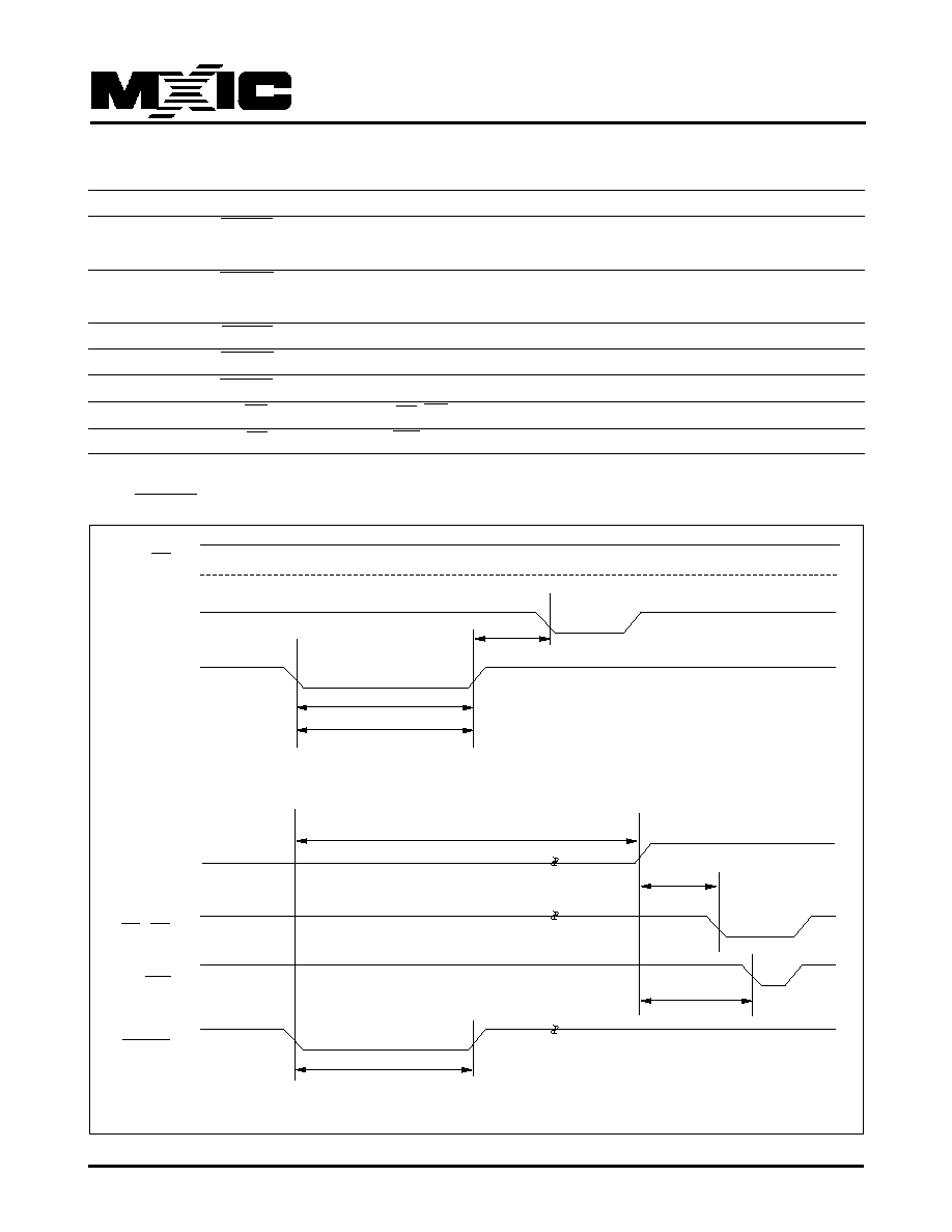
33
P/N:PM1008
REV. 1.1, MAY 28, 2004
MX29LV320AT/B
Fig 3. RESET TIMING WAVEFORM
AC CHARACTERISTICS
Parameter
Description
Test Setup
All Speed Options Unit
tREADY1
RESET PIN Low (During Automatic Algorithms)
MAX
20
us
to Read or Write (See Note)
tREADY2
RESET PIN Low (NOT During Automatic
MAX
500
ns
Algorithms) to Read or Write (See Note)
tRP1
RESET Pulse Width (During Automatic Algorithms)
MIN
10
us
tRP2
RESET Pulse Width (NOT During Automatic Algorithms)
MIN
500
ns
tRH
RESET High Time Before Read(See Note)
MIN
70
ns
tRB1
RY/BY Recovery Time(to CE, OE go low)
MIN
0
ns
tRB2
RY/BY Recovery Time(to WE go low)
MIN
50
ns
Note:Not 100% tested
tRH
tRB1
tRB2
tReady1
tRP2
tRP1
tReady2
RY/BY
CE, OE
RESET
Reset Timing NOT during Automatic Algorithms
Reset Timing during Automatic Algorithms
RY/BY
CE, OE
RESET
WE
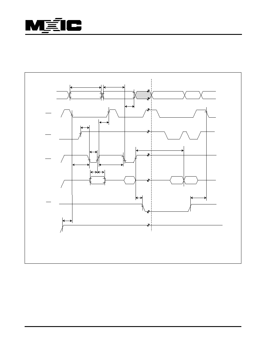
34
P/N:PM1008
REV. 1.1, MAY 28, 2004
MX29LV320AT/B
ERASE/PROGRAM OPERATION
Fig 4. AUTOMATIC CHIP ERASE TIMING WAVEFORM
tWC
Address
OE
CE
55h
2AAh
SA
10h
In
Progress Complete
VA
VA
NOTES:
SA=sector address(for Sector Erase), VA=Valid Address for reading status data(see "Write Operation Status").
tAS
tAH
555h for chip erase
tGHWL
tCH
tWP
tDS
tDH
tWHWH2
Read Status Data
Erase Command Sequence(last two cycle)
tBUSY
tRB
tCS
tWPH
tVCS
WE
Data
RY/BY
VCC

35
P/N:PM1008
REV. 1.1, MAY 28, 2004
MX29LV320AT/B
Fig 5. AUTOMATIC CHIP ERASE ALGORITHM FLOWCHART
START
Write Data AAH Address 555H
Write Data 55H Address 2AAH
Write Data AAH Address 555H
Write Data 80H Address 555H
YES
Write Data 10H Address 555H
Write Data 55H Address 2AAH
DATA = FFh ?
YES
Auto Erase Completed
Data Poll
from system
No

36
P/N:PM1008
REV. 1.1, MAY 28, 2004
MX29LV320AT/B
Fig 6. AUTOMATIC SECTOR ERASE TIMING WAVEFORM
tWC
Address
OE
CE
55h
2AAh
Sector
Address 1
Sector
Address 0
30h
In
Progress Complete
VA
VA
30h
NOTES:
SA=sector address(for Sector Erase), VA=Valid Address for reading status data(see "Write Operation Status").
Sector
Address n
tAS
tAH
tBAL
tGHWL
tCH
tWP
tDS tDH
tWHWH2
Read Status Data
Erase Command Sequence(last two cycle)
tBUSY
tRB
tCS
tWPH
tVCS
WE
Data
RY/BY
VCC
30h

37
P/N:PM1008
REV. 1.1, MAY 28, 2004
MX29LV320AT/B
Fig 7. AUTOMATIC SECTOR ERASE ALGORITHM FLOWCHART
START
Write Data AAH Address 555H
Write Data 55H Address 2AAH
Write Data AAH Address 555H
Write Data 80H Address 555H
Write Data 30H Sector Address
Write Data 55H Address 2AAH
Auto Sector Erase Completed
Data Poll from System
YES
NO
Data=FFh?
Last Sector
to Erase ?
NO
YES

38
P/N:PM1008
REV. 1.1, MAY 28, 2004
MX29LV320AT/B
Fig 8. ERASE SUSPEND/RESUME FLOWCHART
START
Write Data B0H
Toggle Bit checking Q6
not toggled
ERASE SUSPEND
YES
NO
Write Data 30H
Continue Erase
Reading or
Programming End
Read Array or
Program
Another
Erase Suspend ?
NO
YES
YES
NO
ERASE RESUME

39
P/N:PM1008
REV. 1.1, MAY 28, 2004
MX29LV320AT/B
Fig 9. AUTOMATIC PROGRAM TIMING WAVEFORMS
Fig 10. Accelerated Program Timing Diagram
tWC
Address
OE
CE
A0h
555h
PA
PD
Status
DOUT
PA
PA
NOTES:
1.PA=Program Address, PD=Program Data, DOUT is the true data the program address
tAS
tAH
tGHWL
tCH
tWP
tDS
tDH
tWHWH1
Read Status Data (last two cycle)
Program Command Sequence(last two cycle)
tBUSY
tRB
tCS
tWPH
tVCS
WE
Data
RY/BY
VCC
WP/ACC
tVHH
VHH
(11.5V ~ 12.5V)
VIL or VIH
VIL or VIH
tVHH

40
P/N:PM1008
REV. 1.1, MAY 28, 2004
MX29LV320AT/B
Fig 11. CE CONTROLLED WRITE TIMING WAVEFORM
tWC
tWH
tGHEL
tWHWH1 or 2
tCP
Address
WE
OE
CE
Data
Q7
PA
Data Polling
DOUT
RESET
RY/BY
NOTES:
1. PA=Program Address, PD=Program Data, DOUT=Data Out, Q7=complement of data written to device.
2. Figure indicates the last two bus cycles of the command sequence.
tAH
tAS
PA for program
SA for sector erase
555 for chip erase
tRH
tDH
tDS
tWS
A0 for program
55 for erase
tCPH
tBUSY
PD for program
30 for sector erase
10 for chip erase
555 for program
2AA for erase

41
P/N:PM1008
REV. 1.1, MAY 28, 2004
MX29LV320AT/B
Fig 12. AUTOMATIC PROGRAMMING ALGORITHM FLOWCHART
START
Write Data AAH Address 555H
Write Data 55H Address 2AAH
Write Program Data/Address
Write Data A0H Address 555H
YES
Verify Data OK ?
YES
Auto Program Completed
Data Poll
from system
Increment
Address
Last Address ?
No
No

42
P/N:PM1008
REV. 1.1, MAY 28, 2004
MX29LV320AT/B
SECTOR GROUP PROTECT/CHIP UNPROTECT
Fig 13. Sector Group Protect/Chip Unprotect Waveform (RESET Control)
Note:
1. For sector group protect A6=0, A1=1, A0=0 ; for chip unprotect A6=1, A1=1, A0=0
Sector Group Protect: 150us
Chip Unprotect: 15ms
1us
VID
VIH
Data
SA, A6
A1, A0
CE
WE
OE
Valid (note2)
Valid (note2)
Valid (note2)
Status
Sector Group Protect or Chip Unprotect
40h
60h
60h
Verify
RESET

43
P/N:PM1008
REV. 1.1, MAY 28, 2004
MX29LV320AT/B
Fig 14. IN-SYSTEM SECTOR GROUP PROTECT/CHIP UNPROTECT ALGORITHMS WITH RESET=VID
START
PLSCNT=1
RESET=VID
Wait 1us
Set up sector address
Sector Protect:
Write 60h to sector
address with
A6=0, A1=1, A0=0
Wait 150us
Verify Sector Protect:
Write 40h to sector
address with
A6=0, A1=1, A0=0
Read from
sector address
with
A6=0, A1=1, A0=0
Reset
PLSCNT=1
Remove VID from RESET
Write reset command
Sector Protect
Algorithm
Chip Unprotect
Algorithm
Sector Protect complete
Remove VID from RESET
Write reset command
Chip Unprotect complete
Device failed
Temporary Sector
Unprotect Mode
Increment PLSCNT
Increment PLSCNT
First Write
Cycle=60h?
Set up first sector address
Protect all sectors:
The indicated portion of
the sector protect algorithm
must be performed
for all unprotected sectors
prior to issuing the first
sector unprotect address
Chip Unprotect:
Write 60h to sector
address with
A6=1, A1=1, A0=0
Wait 15ms
Verify Sector Unprotect:
Write 40h to sector
address with
A6=1, A1=1, A0=0
Read from
sector address
with
A6=1, A1=1, A0=0
Data=01h?
PLSCNT=25?
Device failed
START
PLSCNT=1
RESET=VID
Wait 1us
First Write
Cycle=60h?
All sectors
protected?
Data=00h?
PLSCNT=1000?
Last sector
verified?
Yes
Yes
Yes
No
No
No
Yes
Yes
Yes
Yes
Yes
Yes
No
No
No
No
No
No
Protect another
sector?
Reset
PLSCNT=1
Temporary Sector
Unprotect Mode

44
P/N:PM1008
REV. 1.1, MAY 28, 2004
MX29LV320AT/B
Fig 15. TEMPORARY SECTOR GROUP UNPROTECT WAVEFORMS
RESET
CE
WE
RY/BY
tVIDR
12V
0 or 3V
VIL or VIH
tRSP
tVIDR
Program or Erase Command Sequence
Table 7. TEMPORARY SECTOR GROUP UNPROTECT
Parameter Std. Description
Test Setup
All Speed Options Unit
tVIDR
VID Rise and Fall Time (See Note)
Min
500
ns
tRSP
RESET Setup Time for Temporary Sector Unprotect
Min
4
us
Note:
Not 100% tested

45
P/N:PM1008
REV. 1.1, MAY 28, 2004
MX29LV320AT/B
Fig 16. TEMPORARY SECTOR GROUP UNPROTECT FLOWCHART
Start
RESET = VID (Note 1)
Perform Erase or Program Operation
RESET = VIH
Temporary Sector Unprotect Completed(Note 2)
Operation Completed
2. All previously protected sectors are protected again.
Note : 1. All protected sectors are temporary unprotected. VID=11.5V~12.5V.
(if WP/ACC=VIL, outermost boot sectors will remain protected)
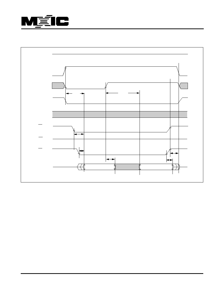
46
P/N:PM1008
REV. 1.1, MAY 28, 2004
MX29LV320AT/B
Fig 17. SILICON ID READ TIMING WAVEFORM
tACC
tCE
tACC
tOE
tOH
tOH
tDF
DATA OUT
C2H
A7H (TOP boot)
A8H (Bottom boot)
VID
VIH
VIL
ADD
A9
ADD
CE
A1
OE
WE
ADD
A0
DATA OUT
DATA
Q0-Q7
VCC
3V
VIH
VIL
VIH
VIL
VIH
VIL
VIH
VIL
VIH
VIL
VIH
VIL
VIH
VIL
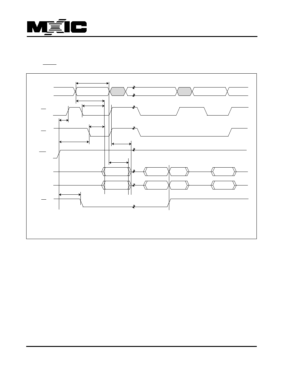
47
P/N:PM1008
REV. 1.1, MAY 28, 2004
MX29LV320AT/B
WRITE OPERATION STATUS
Fig 18. DATA POLLING TIMING WAVEFORMS (DURING AUTOMATIC ALGORITHMS)
NOTES:
VA=Valid address. Figure shows are first status cycle after command sequence, last status read cycle, and array data read cycle.
tDF
tCE
tCH
tOE
tOEH
tACC
tRC
tOH
Address
CE
OE
WE
Q7
Q0-Q6
RY/BY
tBUSY
Status Data
Status Data
Status Data
Complement
True
Valid Data
VA
VA
High Z
High Z
Valid Data
True

48
P/N:PM1008
REV. 1.1, MAY 28, 2004
MX29LV320AT/B
Fig 19. Data Polling Algorithm
START
Read Q7~Q0
Add. = VA (1)
Yes
Yes
Yes
No
No
No
Q7 = Data ?
Q7 = Data ?
Q5 = 1 ?
Read Q7~Q0
Add. = VA
PASS
FAIL
(2)
Notes:
1. VA=valid address for programming or erasure.
2. Q7 should be rechecked even Q5="1" because Q7 may change simultaneously with Q5.

49
P/N:PM1008
REV. 1.1, MAY 28, 2004
MX29LV320AT/B
Fig 20. TOGGLE BIT TIMING WAVEFORMS (DURING AUTOMATIC ALGORITHMS)
NOTES:
VA=Valid address; not required for Q6. Figure shows first two status cycle after command sequence, last status read cycle, and
array data read cycle.
tDF
tCE
tCH
tOE
tOEH
tACC
tRC
tOH
Address
CE
OE
WE
Q6/Q2
RY/BY
tBUSY
Valid Status
(first read)
Valid Status
(second read)
(stops toggling)
Valid Data
VA
VA
VA
VA
Valid Data
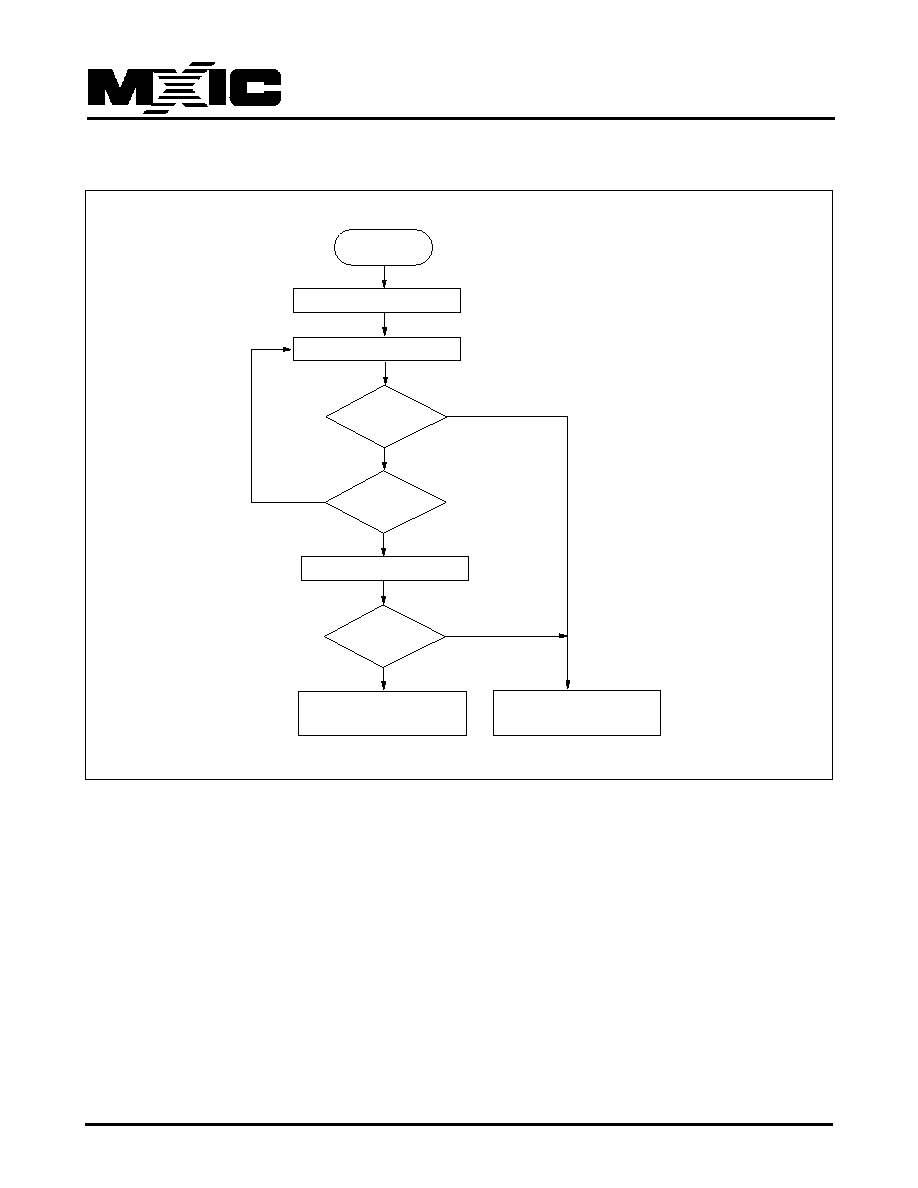
50
P/N:PM1008
REV. 1.1, MAY 28, 2004
MX29LV320AT/B
START
Read Q7~Q0
Read Q7~Q0
YES
NO
Toggle Bit Q6
=Toggle?
Q5=1?
YES
NO
(Note 1)
Read Q7~Q0 Twice
(Note 1,2)
Toggle Bit Q6=
Toggle?
Program/Erase Operation Not
Complete, Write Reset Command
YES
Program/Erase Operation Complete
Fig 21. Toggle Bit Algorithm
Note:
1. Read toggle bit twice to determine whether or not it is toggling.
2. Recheck toggle bit because it may stop toggling as Q5 changes to "1".

51
P/N:PM1008
REV. 1.1, MAY 28, 2004
MX29LV320AT/B
Fig 22. Q6 versus Q2
NOTES:
The system can use OE or CE to toggle Q2/Q6, Q2 toggles only when read at an address within an erase-suspended
WE
Enter Embedded
Erasing
Erase
Suspend
Enter Erase
Suspend Program
Erase
Suspend
Program
Erase Suspend
Read
Erase Suspend
Read
Erase
Erase
Resume
Erase
Complete
Erase
Q6
Q2

52
P/N:PM1008
REV. 1.1, MAY 28, 2004
MX29LV320AT/B
Figure 23. BYTE TIMING WAVEFORM FOR READ OPERATIONS (BYTE switching from byte
mode to word mode)
tFHQV
tELFH
DOUT
(Q0-Q7)
DOUT
(Q0-Q14)
VA
DOUT
(Q15)
CE
OE
BYTE
Q0~Q14
Q15/A-1
AC CHARACTERISTICS
WORD/BYTE CONFIGURATION (BYTE)
Parameter
Description
Speed Options
Unit
JEDEC
Std
-70
-90
tELFL/tELFH
CE to BYTE Switching Low or High
Max 5
ns
tFLQZ
BYTE Switching Low to Output HIGH Z
Max
25
30
ns
tFHQV
BYTE Switching High to Output Active
Min
70
90
ns
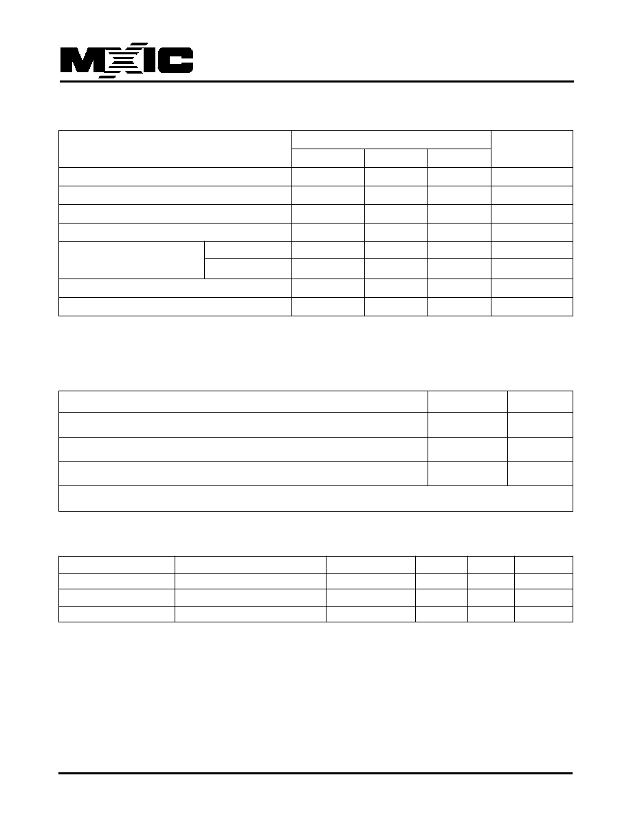
53
P/N:PM1008
REV. 1.1, MAY 28, 2004
MX29LV320AT/B
MIN.
MAX.
Input Voltage with respect to GND on all pins except I/O pins
-1.0V
12.5V
Input Voltage with respect to GND on all I/O pins
-1.0V
Vcc + 1.0V
VCC Current
-100mA
+100mA
Includes all pins except Vcc. Test conditions: Vcc = 3.0V, one pin at a time.
LIMITS
PARAMETER
MIN.
TYP.(2)
MAX.
UNITS
Sector Erase Time
0.9
15
sec
Chip Erase Time
35
50
sec
Byte Programming Time
9
300
us
Word Program Time
11
360
us
Chip Programming Time
Byte Mode
36
108
sec
Word Mode
24
72
sec
Accelerated Byte/Word Program Time
7
210
us
Erase/Program Cycles
100,000
Cycles
LATCH-UP CHARACTERISTICS
ERASE AND PROGRAMMING PERFORMANCE(1)
Note:
1.Not 100% Tested, Excludes external system level over head.
2.Typical values measured at 25
∞
C,3.3V.
Parameter Symbol
Parameter Description
Test Set
TYP
MAX
UNIT
CIN
Input Capacitance
VIN=0
6
7.5
pF
COUT
Output Capacitance
VOUT=0
8.5
12
pF
CIN2
Control Pin Capacitance
VIN=0
7.5
9
pF
TSOP PIN CAPACITANCE
Notes:
1. Sampled, not 100% tested.
2. Test conditions TA=25
∞
C, f=1.0MHz

54
P/N:PM1008
REV. 1.1, MAY 28, 2004
MX29LV320AT/B
ORDERING INFORMATION
PLASTIC PACKAGE
PART NO.
ACCESS TIME
Ball Pitch/
PACKAGE
Remark
(ns)
Ball Size
MX29LV320ATTC-70
70
-
48 Pin TSOP
MX29LV320ABTC-70
70
-
48 Pin TSOP
MX29LV320ATTI-70
70
-
48 Pin TSOP
MX29LV320ABTI-70
70
-
48 Pin TSOP
MX29LV320ATTC-90
90
-
48 Pin TSOP
MX29LV320ABTC-90
90
-
48 Pin TSOP
MX29LV320ATTI-90
90
-
48 Pin TSOP
MX29LV320ABTI-90
90
-
48 Pin TSOP
MX29LV320ATXBC-70
70
0.8mm/0.3mm
48-Ball CSP
MX29LV320ABXBC-70
70
0.8mm/0.3mm
48-Ball CSP
MX29LV320ATXEC-70
70
0.8mm/0.4mm
48-Ball CSP
MX29LV320ABXEC-70
70
0.8mm/0.4mm
48-Ball CSP
MX29LV320ATXBI-70
70
0.8mm/0.3mm
48-Ball CSP
MX29LV320ABXBI-70
70
0.8mm/0.3mm
48-Ball CSP
MX29LV320ATXEI-70
70
0.8mm/0.4mm
48-Ball CSP
MX29LV320ABXEI-70
70
0.8mm/0.4mm
48-Ball CSP
MX29LV320ATXBC-90
90
0.8mm/0.3mm
48-Ball CSP
MX29LV320ABXBC-90
90
0.8mm/0.3mm
48-Ball CSP
MX29LV320ATXEC-90
90
0.8mm/0.4mm
48-Ball CSP
MX29LV320ABXEC-90
90
0.8mm/0.4mm
48-Ball CSP
MX29LV320ATXBI-90
90
0.8mm/0.3mm
48-Ball CSP
MX29LV320ABXBI-90
90
0.8mm/0.3mm
48-Ball CSP
MX29LV320ATXEI-90
90
0.8mm/0.4mm
48-Ball CSP
MX29LV320ABXEI-90
90
0.8mm/0.4mm
48-Ball CSP

55
P/N:PM1008
REV. 1.1, MAY 28, 2004
MX29LV320AT/B
PART NO.
ACCESS TIME
Ball Pitch/
PACKAGE
Remark
(ns)
Ball Size
MX29LV320ATTC-70G
70
-
48 Pin TSOP
Pb-free
MX29LV320ABTC-70G
70
-
48 Pin TSOP
Pb-free
MX29LV320ATTI-70G
70
-
48 Pin TSOP
Pb-free
MX29LV320ABTI-70G
70
-
48 Pin TSOP
Pb-free
MX29LV320ATTC-90G
90
-
48 Pin TSOP
Pb-free
MX29LV320ABTC-90G
90
-
48 Pin TSOP
Pb-free
MX29LV320ATTI-90G
90
-
48 Pin TSOP
Pb-free
MX29LV320ABTI-90G
90
-
48 Pin TSOP
Pb-free
MX29LV320ATXBC-70G
70
0.8mm/0.3mm
48-Ball CSP
Pb-free
MX29LV320ABXBC-70G
70
0.8mm/0.3mm
48-Ball CSP
Pb-free
MX29LV320ATXEC-70G
70
0.8mm/0.4mm
48-Ball CSP
Pb-free
MX29LV320ABXEC-70G
70
0.8mm/0.4mm
48-Ball CSP
Pb-free
MX29LV320ATXBI-70G
70
0.8mm/0.3mm
48-Ball CSP
Pb-free
MX29LV320ABXBI-70G
70
0.8mm/0.3mm
48-Ball CSP
Pb-free
MX29LV320ATXEI-70G
70
0.8mm/0.4mm
48-Ball CSP
Pb-free
MX29LV320ABXEI-70G
70
0.8mm/0.4mm
48-Ball CSP
Pb-free
MX29LV320ATXBC-90G
90
0.8mm/0.3mm
48-Ball CSP
Pb-free
MX29LV320ABXBC-90G
90
0.8mm/0.3mm
48-Ball CSP
Pb-free
MX29LV320ATXEC-90G
90
0.8mm/0.4mm
48-Ball CSP
Pb-free
MX29LV320ABXEC-90G
90
0.8mm/0.4mm
48-Ball CSP
Pb-free
MX29LV320ATXBI-90G
90
0.8mm/0.3mm
48-Ball CSP
Pb-free
MX29LV320ABXBI-90G
90
0.8mm/0.3mm
48-Ball CSP
Pb-free
MX29LV320ATXEI-90G
90
0.8mm/0.4mm
48-Ball CSP
Pb-free
MX29LV320ABXEI-90G
90
0.8mm/0.4mm
48-Ball CSP
Pb-free
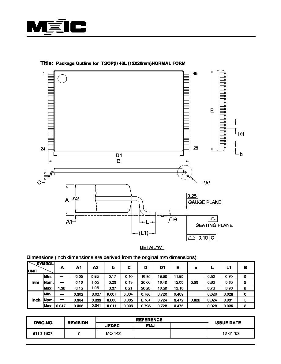
56
P/N:PM1008
REV. 1.1, MAY 28, 2004
MX29LV320AT/B
PACKAGE INFORMATION

57
P/N:PM1008
REV. 1.1, MAY 28, 2004
MX29LV320AT/B

58
P/N:PM1008
REV. 1.1, MAY 28, 2004
MX29LV320AT/B

59
P/N:PM1008
REV. 1.1, MAY 28, 2004
MX29LV320AT/B
REVISION HISTORY
Revision No. Description
Page
Date
1.0
1. Removed "Advanced Information" on page 1
P1
JAN/30/2004
1.1
1. To removed data retention information
P53
MAY/28/2004

MX29LV320AT/B
M
ACRONIX
I
NTERNATIONAL
C
O.,
L
TD.
Headquarters:
TEL:+886-3-578-6688
FAX:+886-3-563-2888
Europe Office :
TEL:+32-2-456-8020
FAX:+32-2-456-8021
Hong Kong Office :
TEL:+86-755-834-335-79
FAX:+86-755-834-380-78
Japan Office :
Kawasaki Office :
TEL:+81-44-246-9100
FAX:+81-44-246-9105
Osaka Office :
TEL:+81-6-4807-5460
FAX:+81-6-4807-5461
Singapore Office :
TEL:+65-6346-5505
FAX:+65-6348-8096
Taipei Office :
TEL:+886-2-2509-3300
FAX:+886-2-2509-2200
M
ACRONIX
A
MERICA,
I
NC.
TEL:+1-408-262-8887
FAX:+1-408-262-8810
http : //www.macronix.com
MACRONIX INTERNATIONAL CO., LTD. reserves the right to change product and specifications without notice.