
MDT10P56
This specification are subject to be changed without notice. Any latest information please preview
http;//www.mdtic.com.tw
P. 1
2003/ 5 Ver. 1.1
1. General Description
This EPROM-Based 8-bit micro-controller uses a fully
static CMOS technology process to achieve higher
speed and smaller size with the low power
consump-tion and high noise immunity. On chip
memory inclu-des 1K words of ROM, and 72 bytes of
static RAM.
2. Features
The followings are some of the features on the
hardware and software :
u
Fully COMS static design
u
8-bit data bus
u
On chip EPROM size : 1K words
u
Internal RAM size : 72 bytes
u
36 single word instructions
u
14-bit instructions
u
2-level stacks
u
Operating voltage : 2.5 V ~ 6.0 V
u
Operating frequency : 0 ~ 20 MHz
u
The most fast execution time is 200 ns under
20 MHz in all single cycle instructions except
the branch instruction
u
Addressing modes include direct, indirect and
relative addressing modes
u
Power-on Reset
u
Sleep Mode for power saving
u
5 types of oscillator can be selected by
programming option:
INTRC
Internal 4 MHz RC oscillator
RC
Low cost RC oscillator
LFXT
Low frequency crystal oscillator
XTAL
Standard crystal oscillator
HFXT
High frequency crystal oscillator
u
3 oscillator start-up time can be selected by
programming option:
20 ms, 40 ms, 80 ms
u
8-bit real time clock/counter(RTCC) with 8-bit
programmable prescaler
u
On-chip RC oscillator based Watchdog
Timer(WDT)
u
Wake-up from sleep on pin change
3. Applications
The application areas of this MDT10P56 range from
appliance motor control and high speed automotive
to low power remote transmitters/receivers, small
instruments, chargers, toy, automobile and PC
peripheral ... etc.

MDT10P56
This specification are subject to be changed without notice. Any latest information please preview
http;//www.mdtic.com.tw
P. 2
2003/ 5 Ver. 1.1
MDT10P56A3P/MDT10P56A3S
PC7 1
18 PB7
PC6 2
17 PB6
VDD 3
16 VSS
PB5 4
15 PB0
PB4 5
14 PB1
MCLR 6
13 PB2
7 12 PC0
PC1
PC5/RTCC
PC4
PC3
8
9
11
10 PC2
MDT10P56A4P/MDT10P56A4S
PC7 1
18 PB7
PC6 2
17 PB6
VDD 3
16 VSS
OSC1 4
15 PB0
OSC2/PB4 5
14 PB1
MCLR 6
13 PB2
7 12 PC0
PC1
PC5/RTCC
PC4
PC3
8
9
11
10 PC2
4. Pin Assignment
MDT10P56A1P/MDT10P56A1S
PC7 1
18 PB7
PC6 2
17 PB6
VDD 3
16 VSS
PB5 4
15 PB0
PB4 5
14 PB1
PB3 6
13 PB2
7 12 PC0
PC1
PC5/RTCC
PC4
PC3
8
9
11
10 PC2
MDT10P56A2P/MDT10P56A2S
PC7 1
18 PB7
PC6 2
17 PB6
VDD 3
16 VSS
OSC1 4
15 PB0
OSC2/PB4 5
14 PB1
PB3 6
13 PB2
7 12 PC0
PC1
PC5/RTCC
PC4
PC3
8
9
11
10 PC2
5. Pin Function Description
Pin Name
I/O
Function Description
PB7~0
I/O
Port B, TTL input level
PB3 input only.
PC7~0
I/O
Port C, TTL input level
PC5/RTCC
I/O
Real Time Clock/Counter, Schmitt Trigger input levels
/MCLR
I
Master Clear, Schmitt Trigger input levels
OSC1
I
Oscillator Input
OSC2
O
Oscillator Output
V
dd
Power supply
V
ss
Ground
MDT10P56
This specification are subject to be changed without notice. Any latest information please preview
http;//www.mdtic.com.tw
P. 3
2003/ 5 Ver. 1.1
6. Memory Map
(A) Register Map
Address
Description
00
Indirect Addressing Register
01
RTCC
02
PC
03
STATUS
04
MSR
06
Port B
07
Port C
08~1F
30~3F
50~5F
70~7F
General purpose registers
(1)IAR ( Indirect Address Register) : R0
(2) RTCC (Real Time Counter/Counter Register) : R1
(3) PC (Program Counter) : R2
Write PC, CALL --- always 0
JUMP --- from instruction word
RTIW, RET --- from STACK
A9
A8
A7~A0
Write PC, JUMP, CALL --- from STATUS b5
RTIW, RET --- from STACK
Write PC --- from ALU
JUMP, CALL --- from instruction word
RTIW, RET --- from STACK

MDT10P56
This specification are subject to be changed without notice. Any latest information please preview
http;//www.mdtic.com.tw
P. 4
2003/ 5 Ver. 1.1
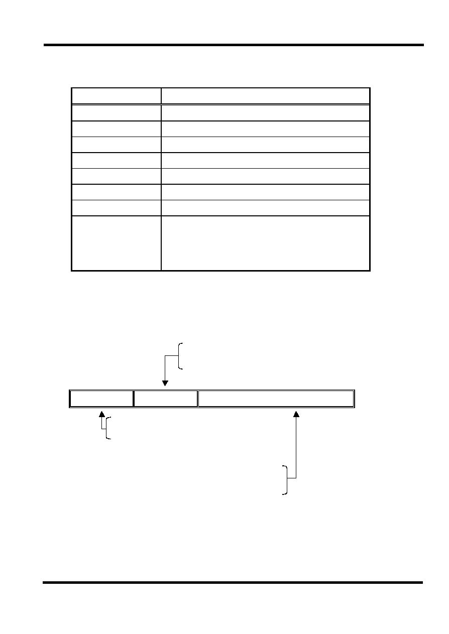
(4) STATUS (Status register) : R3
Bit
Symbol
Function
0
1
2
3
4
5
6
7
C
HC
Z
PF
TF
PAGE
----
PCWUF
Carry bit
Half Carry bit
Zero bit
Power down bit
WDT Timer overflow Flag bit
ROM page select bit :
Unimplemented
Pin change wake up from sleep
(5) MSR (Memory Bank Select Register) : R4
b7
b6
b5
b4
b3
b2
b1
b0
Read only "1" BANK Select
Indirect Addressing Mode
(6) PORT B : R6
PB7~PB0, I/O Register
PB3 input only.
(6) PORT C: R7
PC7~PC0, I/O Register.
(7) TMR (Time Mode Register)
Bit
Symbol
Function
Prescaler Value
RTCC rate
WDT rate
2
--
0
PS2
--
0
0 0 0
0 0 1
0 1 0
0 1 1
1 0 0
1 0 1
1 1 0
1 1 1
1 : 2
1 : 4
1 : 8
1 : 16
1 : 32
1 : 64
1 : 128
1 : 256
1 : 1
1 : 2
1 : 4
1 : 8
1 : 16
1 : 32
1 : 64
1 : 128
3
PSC
Prescaler assignment bit :
0
--
RTCC
1
--
Watchdog Timer
4
TCE
RTCC signal Edge :
0
--
Increment on low-to-high transition on RTCC pin
1
--
Increment on high-to-low transition on RTCC pin

MDT10P56
This specification are subject to be changed without notice. Any latest information please preview
http;//www.mdtic.com.tw
P. 5
2003/ 5 Ver. 1.1
Bit
Symbol
Function
Prescaler Value
RTCC rate
WDT rate
5
TCS
RTCC signal set :
0
--
Internal instruction cycle clock
1
--
Transition on RTCC pin
6
PBPHB
PortB pull-high :
0
--
Enable
1
--
Disable
7
PBWUB
PortB wake-up :
0
--
Enable
1
--
Disable
(8) CPIO B (Control Port I/O Mode Register)
The CPIO register is "write-only"
"0", I/O pin in output mode;
"1", I/O pin in input mode.
(9) CPIO C (Control Port I/O Mode Register)
The CPIO register is "write-only"
"0", I/O pin in output mode;
"1", I/O pin in input mode.
(10) Configurable options for EPROM (Set by writer) :
Oscillator Type
Oscillator Start-up Time
INTRC Oscillator
20ms,40ms,80ms
RC Oscillator
20ms,40ms,80ms
HFXT Oscillator
20ms,40ms,80ms
XTAL Oscillator
20ms,40ms,80ms
LFXT Oscillator
20ms,40ms,80ms
Watchdog Timer control
Watchdog timer disable all the time
Watchdog timer enable all the time
Security state
Security weak Disable
Security Disable
Security Enable
The default security state of EPROM is weak disable. Once the IC was set to
enable or disable, it's forbidden to change.