MLX90401
Brushless DC Motor Controller
3901090401
Page 1 of 12
Data Sheet
Rev. 002
Aug/02
Features and Benefits
∑
12V to 40V Operating Range
∑
On-Chip "Boost" Voltage Allows Use of All N-Channel Drivers
∑
Undervoltage Lockout
∑
On-Chip PWM Oscillator
∑
PWM Speed Control via Bottom Drivers
∑
Forward and Reverse Control
∑
BVDSS > 60V
∑
Selectable 60∞ or 120∞ Sensor Electrical Phasings
Applications
∑
Brushless DC Motor Control
Ordering Information
Part No.
Temperature Suffix
Package Code
MLX90401
E(-40∞C to 85∞C)
DF (24 Lead SOIC)
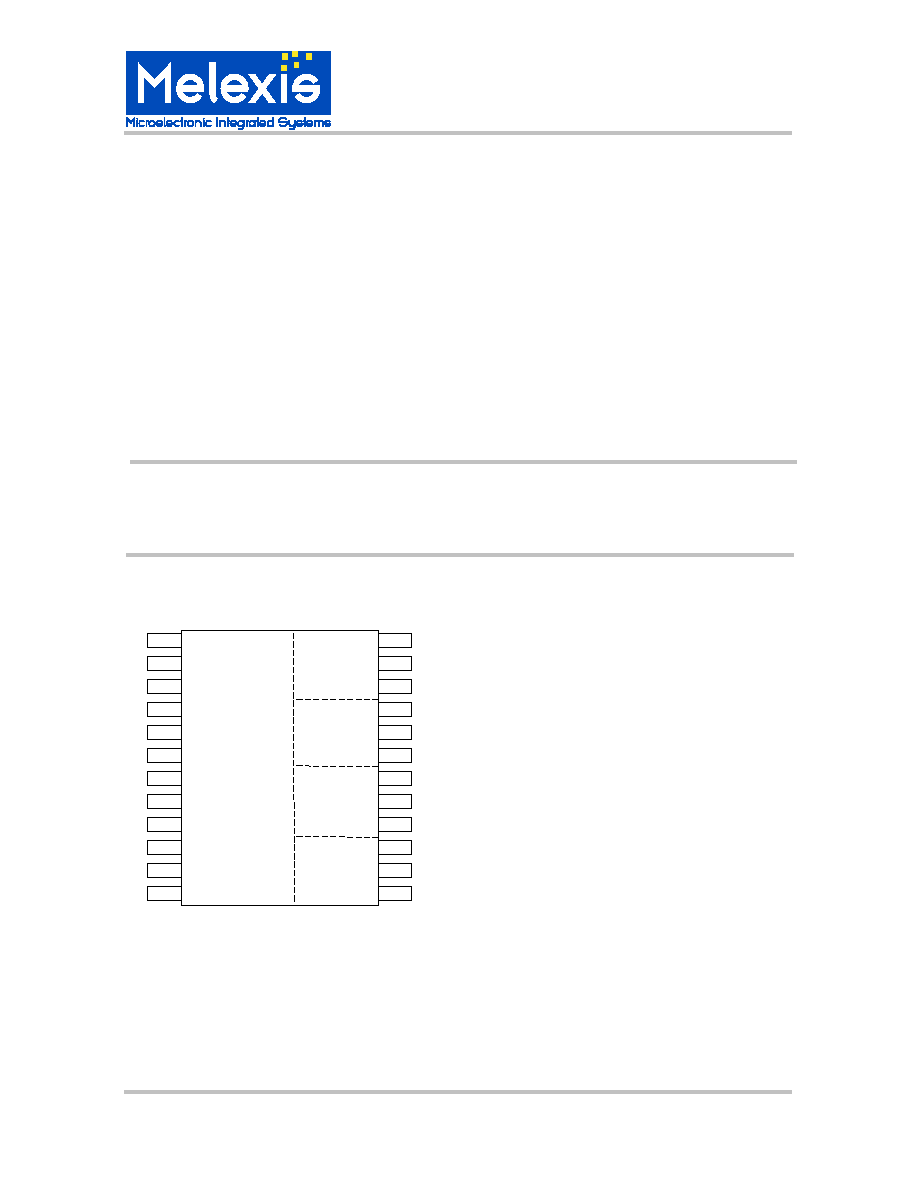
1. Pin connections
2. Description
The MLX90401 is a three-phase brushless DC
motor controller, designed to meet the needs of
high volume, low cost motors with 60
o
or 120∞
electrical sensor phasings which do not require
the expensive options needed for servo or other
closed loop applications.
The use of CMOS technology offers dense logic
as well as high voltage (60V) driver capabilities.
The use of discrete low cost N-channel power
FETs reduces overall system cost and the
device provides all of the logic necessary to
interface Hall-effect position sensors to N-
channel power FETs. Upper N-channel power
FETs require a gate drive in excess of the
supply voltage V+, and with the device's on-chip
"boost" voltage, the use of all N-Channel power
FETs is allowed.
Control inputs are provided for motor speed,
forward or reverse direction, disable, and
braking. Also 60∞ or 120∞ electrical sensor
phasings can be set externally.
The device is offered in a 24 Lead "Wide-Body"
SOIC package (DF).
1
2
3
4
5
6
7
8
9
10
11
12
24
23
22
21
20
19
18
17
16
15
14
13
Supply Voltage
Cap Boost "A"
V
REF
Out
Hall "A" Input
Hall "B" Input
Hall "C" Input
Fwd/Rev Input
Speed Adjust Input / Disable
Oscillator R/C
/Brake Input
Analog Ground
60∞/120∞ Select Input
Power Ground
Gate Top "A"
Feedback "A"
Cap Boost "B"
Gate Top "B"
Feedback "B"
Gate Bottom "B"
Gate Top "C"
Feedback "C"
Gate Bottom "C"
Cap Boost "C"
Gate Bottom "A"

MLX90401
Brushless DC Motor Controller
3901090401
Page 2-2 of 12
Data Sheet
Rev. 002
Aug/02
TABLE OF CONTENTS
FEATURES AND BENEFITS .................................................................................................................. 1
APPLICATIONS ...................................................................................................................................... 1
ORDERING INFORMATION.................................................................................................................... 1
1.
PIN CONNECTIONS ..................................................................................................................... 1-1
2.
DESCRIPTION .............................................................................................................................. 2-1
3.
MLX90401 ELECTRICAL SPECIFICATIONS ................................................................................... 3
4.
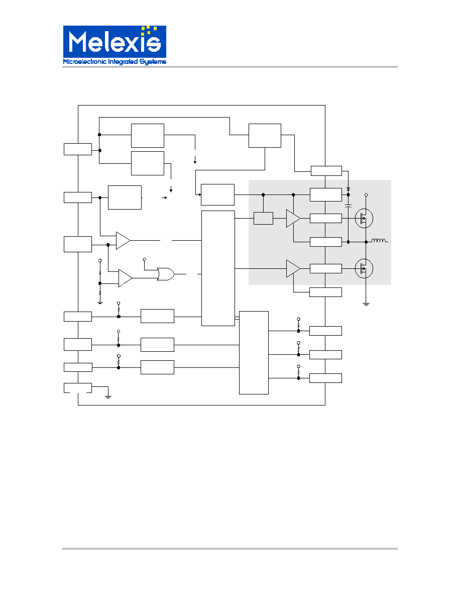
BLOCK DIAGRAM ........................................................................................................................... 5
5.
PIN FUNCTION DESCRIPTION ....................................................................................................... 6
6.
GENERAL DESCRIPTION ............................................................................................................... 7
6.1.
C
OMMUTATION DECODING AND OUTPUT CONTROL LOGIC
...........................................................................7
6.2.
O
SCILLATOR
.............................................................................................................................................7
6.3.
D
ISABLE
...................................................................................................................................................7
6.4.
P
ULSE WIDTH MODULATION
......................................................................................................................7
6.5.
D
RIVE OUTPUTS
........................................................................................................................................8
6.6.
U
NDERVOLTAGE LOCKOUT
.......................................................................................................................8
7.
LOGIC TABLE ................................................................................................................................. 9
8.
ABSOLUTE MAXIMUM RATINGS ................................................................................................... 9
9.
TYPICAL APPLICATION................................................................................................................ 10
10.
APPLICATION COMMENTS .......................................................................................................... 10
10.1.
D
EMO BOARD
.....................................................................................................................................10
11.
RELIABILITY INFORMATION ........................................................................................................ 10
12.
ESD PRECAUTIONS...................................................................................................................... 11
13.
PACKAGE INFORMATION ............................................................................................................ 11
14.
DISCLAIMER ................................................................................................................................. 12
MLX90401
Brushless DC Motor Controller
3901090401
Page 3 of 12
Data Sheet
Rev. 002
Aug/02
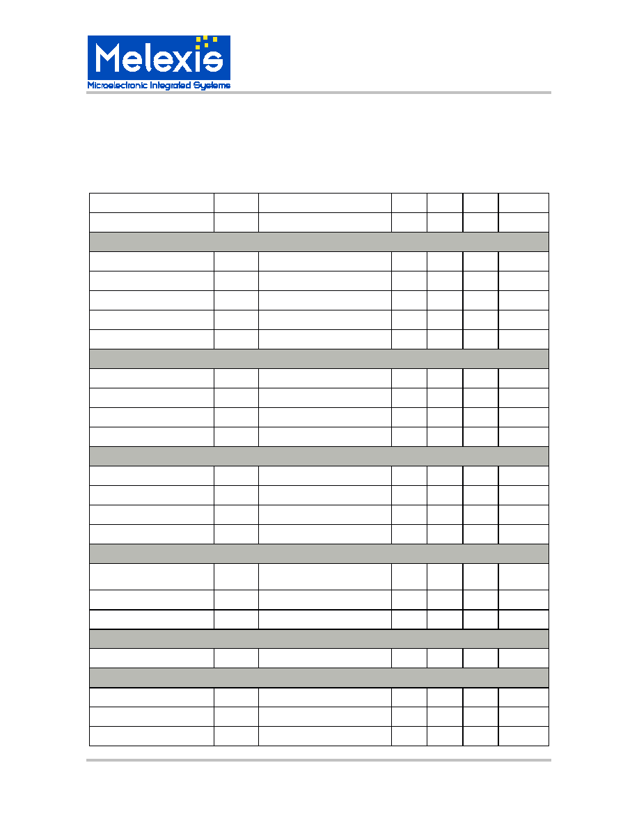
3. MLX90401 Electrical Specifications
DC Operating Parameters T
A
= -40
o
C to 85
o
C, V
DD
= 15V (unless otherwise specified)
Parameter
Symbol
Test Conditions
Min
Typ
Max
Units
Supply Voltage
V
DD
Operating
8
24
44
V
Supply Current
I
DD
Operating
20
35
mA
Voltage Reference, Undervoltage, Oscillator
Output Voltage
V
REF
8
12
15
V
Output Current
I
REF
10
mA
Undervoltage
V
UV
Operating
8
V
Oscillator Frequency
f
OSC
Operating, R
OSC
=10k, C
OSC
=5k
22
25
28
kHz
Frequency Drift
df
OSC
Operating
TBD
Logic Inputs Sensor (Pins 3,4,5), Fwd/Rev (pin 6), /Brake and 60∞/120∞ Select (Pins 9,11) Inputs
High State
V
IH
3.5
V
Low State
V
IL
1.5
V
High State Input Current
I
IH
1.0
mA
Low State Input Current
I
IL
2.0
mA
Disable Input (Pin 7)
High State
V
IH
4.2
V
Low State
V
IL
3.5
V
High State Input Current
I
IH
1.0
mA
Low State Input Current
I
IL
1.0
mA
Debouncing
Debounce Time (60∞/120∞ Select,
Fwd/Rev)
1)
t
delay1
18
25
35
ms
Debounce Time (/Brake)
1)
t
delay2
2
3.2
4.4
ms
Delay after Start-up
2)
t
delay3
18.6
25.6
35.6
ms
Charge Pumps
Output Current
I
OCP
100
µ A
Drivers
Top Output On-Resistance
R
ON,T
I
LOAD
= 50mA
50
Bottom Output On-Resistance
R
ON,B
I
LOAD
= 50mA
50
Rise Time
t
r
150
ns
MLX90401
Brushless DC Motor Controller
3901090401
Page 4 of 12
Data Sheet
Rev. 002
Aug/02
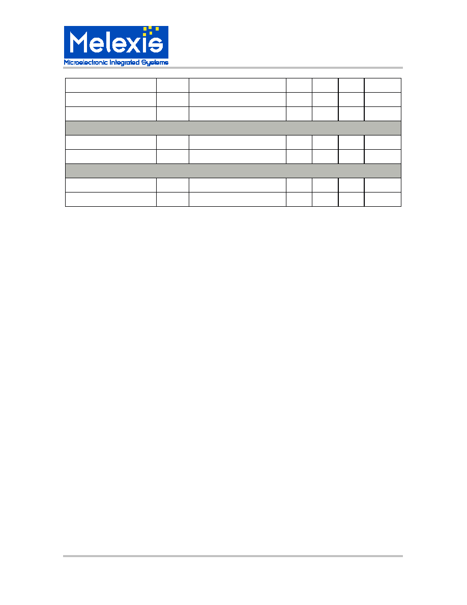
Fall Time
t
f
150
ns
Turn-on Propagation Delay
t
d,on
300
ns
Turn-off Propagation Delay
t
d,off
300
ns
Top Drivers
Leakage Current
I
OFF
V
OUT
= 60V
-10
µ A
Voltage Drop
V
OL
I
OUT
= 50mA
1.3
1.6
V
Bottom Drivers
Voltage Drop High State
V
OH
I
OUT
= 100mA
1.3
1.6
V
Voltage Drop Low State
V
OL
I
OUT
= 100mA
1.3
1.6
V
Note:
1) t
delay1
and t
delay2
depend on f
osc
and timing of the signals to be debounced. 60∞/120∞ Select and
Fwd/Rev are debounced using a clock with a frequency of 256*f
osc
. /Brake is debounced using a clock
with a frequency of 32*f
osc
. Debouncing takes between 2 and 3 clock cycles. Typical example for, say
60∞/120∞ Select: 2.5*256*1/f
osc
= 2.5*256*1/25kHz = 25.6 ms.
2) t
delay3
depends on f
osc
. Precautions are taken that t
delay3
is always larger than t
delay1
, so that there are
only output signals when the chip is in the correct state.