 | –≠–ª–µ–∫—Ç—Ä–æ–Ω–Ω—ã–π –∫–æ–º–ø–æ–Ω–µ–Ω—Ç: MLX90805 | –°–∫–∞—á–∞—Ç—å:  PDF PDF  ZIP ZIP |

MLX90805
Intelligent Triac Controller
3901090805
Page 1 of 16
Data Sheet
Rev. 004
Dec/02
Features and Benefits
!"
"Soft Start" Eliminates Current Surges
!"
Integrated Design Eliminates External Components
!"
Drives Virtually Any Resistive or Inductive Load
!"
Built≠in Thermal Protection
!"
Digital Design For Stable Triac Control
!"
Immune to Lifetime and Thermal Drift
!"
Low Power Consumption
!"
50Hz or 60Hz operation customizable by mask programming
Applications
!"
AC Light Dimmer
!"
Soft-Start AC Motor Controller
!"
Variable-Speed AC Motor Controller
Ordering Information
Part No.
Temperature Suffix
Package Code
Option Code*
MLX90805
C (0∞C to 70∞C)
AA (PDIP-8)
CA
MLX90805
C (0∞C to 70∞C)
DC (SOIC-8)
CA
* See Option Code Table for details
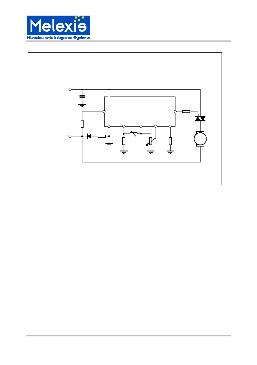
1. Functional Diagram
2. Description
The MLX90805 is a power control IC ideally
suited for control of any resistive or inductive
load regulated by a triac.
The chip was designed primarily for starting and
speed control of AC motors, but will work equally
well with any Inductive or resistive load such as
Incandescent lights.
The chip's primary purpose is to provide a "soft
start" for a motor, preventing current inrush. The
triac is controlled by a linear "ramp" from
minimum to maximum power. Start rate can be
varied from 0.5 sec. to 3 sec, by changing the
option bits.
The secondary function of the MLX90805 is
proper ignition of the triac for inductive and
resistive loads, while keeping the triac's current
consumption to a minimum.
Added features include a frequency locked loop
for stable ignition point.
zero
crossing
detector
Vref
Lookup
ROM
COMP
Options
Logic
Triac driver
Auto
retriggering
ADC
Power monitoring
and reset
Voltage
regulator
Vss
Vdda
THP
FB
ZCD
SET
Vref
Vref/2
90805

MLX90805
Intelligent Triac Controller
3901090805 Page 2 of 16
Data Sheet
Rev. 004
Dec/02
TABLE OF CONTENTS
FEATURES AND BENEFITS........................................................................................................................1
APPLICATIONS ............................................................................................................................................1
ORDERING INFORMATION .........................................................................................................................1
1. FUNCTIONAL DIAGRAM ...................................................................................................................
...1
2. DESCRIPTION ....................................................................................................................................
...1
3. ABSOLUTE MAXIMUM RATINGS........................................................................................................3
4. MLX90805
ELECTRICAL
SPECIFICATIONS.......................................................................................3
5. MLX90805
SPECIFIC
SPECIFICATIONS .............................................................................................3
6. GENERAL
DESCRIPTION ....................................................................................................................5
7. DIGITAL
FEATURES.............................................................................................................................6
8. PINOUT
DESCRIPTION ........................................................................................................................8
9. APPLICATION
INFORMATION.............................................................................................................9
9.1. S
OFT
S
TART
O
NLY
......................................................................................................................................... 9
9.2. S
OFT
S
TART
W
ITH
2-W
IRE
S
ETTING
............................................................................................................ 10
9.3. S
OFT
S
TART
W
ITH
3-W
IRE
S
ETTING
............................................................................................................ 11
9.4. P
ERFORMANCE OF
S
OFT
S
TART
M
ECHANISM
. .............................................................................................. 12
9.5. A
DDITIONAL
A
PPLICATION
I
NFORMATION
................................................................................................... 12
9.6. O
PTION
C
ODE
T
ABLE
................................................................................................................................... 13
10. RELIABILITY INFORMATION.............................................................................................................14
11. ESD PRECAUTIONS ...........................................................................................................................14
12. PACKAGE INFORMATION .................................................................................................................15
13. DISCLAIMER .......................................................................................................................................16

MLX90805
Intelligent Triac Controller
3901090805
Page 3 of 16
Data Sheet
Rev. 004
Dec/02
3. Absolute Maximum Ratings
Supply Voltage, V
DDA
(overvoltage)
18V
Supply Voltage, V
DDA
(operating)
15V
Supply Current, I
DDA
10mA
Maximum chip temperature
150
∞
C
ESD Sensitivity (AEC Q100 002)
2kV
Exceeding the absolute maximum ratings may cause permanent damage. Exposure to absolute-
maximum-rated conditions for extended periods may affect device reliability.
4. MLX90805 Electrical Specifications
DC Operating Parameters T
A
= 0
o
C to 85
o
C, V
DDA
= 13V to 18V (unless otherwise specified)
Parameter Symbol
Test
Conditions
Min
Typ
Max
Units
Ambient temperature
Tamb
0
85
∞C
Maximum chip temperature
Tch
150
∞C
Thermal resistance
Rth
DIP8 or SOP8 package
110
∞C/W
Maximum allowed source
supply current
IDD
Am
Drivers off, all the current flows in
the chip
5
mA
5. MLX90805 Specific Specifications
Power Supply
The MLX90805 ground pin (VSS) must be connected by external series resistors and a rectifier diode to
the AC line. An internal zener function limits the voltage at VDDA to approximately 15V. For proper
operation a decoupling capacitor must be connected between VDDA and VSS.
Parameter Symbol
Test
Conditions
Min
Typ
Max
Units
Voltage applied at the supply pin VDDA
IDDA = 5mA
14
15
16.5
V
Reference Voltage
VDD
IREF = 1.2mA
4.6
5.0
5.4
V
Current consumption
IDDA
VDDA = 14V. Drivers off.
0.6
0.9
1.2
mA
Power On Reset
This block ensures a correct start of the digital part.
The reset signal goes up for VDD > Vdporh and down for VDD < Vdporl.
Parameter Symbol
Test
Conditions
Min
Typ
Max
Units
High level threshold
Vdporh
2.5
V
Low level threshold
Vdporl
2.0
V
Hysteresis Vdphyst
0.5
V

MLX90805
Intelligent Triac Controller
3901090805
Page 4 of 16
Data Sheet
Rev. 004
Dec/02
Analog Power-On Reset
This block tracks the voltage applied at VDDA. The triac firing is permitted if VDDA > Vaporh and is
stopped when VDDA < Vaporl.
Parameter Symbol
Test
Conditions
Min
Typ
Max
Units
High level threshold
Vaporh
12
13 14 V
Low level threshold
Vaporl
9 10 11 V
Hysteresis Vaphyst
2 3 4 V
Zero Cross Detector
This detector contains two comparators with hysteresis. The first comparator has its reference at VDDA.
The reference of the second one is VDDA-1V.
Parameter Symbol
Test
Conditions
Min
Typ
Max
Units
High level threshold 1
Vzc1h
VDDA
+0.1
VDDA
+0.25
VDDA
+0.4
V
Low level threshold 1
Vzc1l
VDDA
-0.1
VDDA
-0.25
VDDA
-0.4
V
High level threshold 2
Vzc2h
VDDA
-1.5
VDDA
-2.1
VDDA
-2.7
V
Low level threshold 2
Vzc2l
VDDA
-2.0
VDDA
-2.6
VDDA
-3.2
V
External resistor
Rzc
Vline = 230VAC typ
470
k
Triac (Ignition) Driver
This driver operates as a switch to fire the triac ON. An external switch is needed to imitate the triac gate
current (aprox. 150
).
Parameter Symbol
Test
Conditions
Min
Typ
Max
Units
Triac gate current
ITRG
VDDA > Vaporh
90
mA
ADC
This is a 4-bit ADC.
Parameter Symbol
Test
Conditions
Min
Typ
Max
Units
Resolution
4 bits
Reference voltage
VREF
4.6 5 5.4 V

MLX90805
Intelligent Triac Controller
3901090805
Page 5 of 16
Data Sheet
Rev. 004
Dec/02
6. General Description
Voltage Regulator
The chip is supplied from the AC line voltage, by
a half wave rectifier. The voltage at pin VDDA is
limited to ~ 15.5V. The digital part and some of
the peripheral blocks are supplied by internally
generated VDD ~ 5V.
Analog Power on Reset
This block tracks the voltage at VDDA, and
permits generation of firing pulses for the triac
only if VDDA > ~13V. It is considered otherwise
that the motor is not properly supplied by the
mains.
Oscillator
There is an on chip oscillator. All timing
constraints inside the chip are derived from this
clock.
FLL
A frequency locked loop circuit is implemented
to obtain a clock frequency from a current
controlled oscillator, by using the mains
frequency as a reference. A successive
approximation algorithm is used at start up to
minimize the time for the oscillator adjustment.
Reference Voltage
This voltage is used to supply the external
potentiometer for the definition of different speed
settings.
ADC
The analog signal from the potentiometer, which
defines the speed setting, is transferred into
digital by a 4-bit ADC. The reference for the
converter is the voltage used to supply the
potentiometer.
ROM
The digital words from the ADC act as the
address of a ROM table in which the different
firing angles are programmed. This means that
16 different firing angles can be selected.
Zero Cross
This block detects the moments when mains
voltage crosses zero level. An accurate
detection allows good synchronization, so firing
pulses driving the triac can be generated at the
right moment.
Logic
This block performs all control functions to
realize time synchronization, smooth soft start,
and proper triac firing, so that motor runs at a
defined speed.
Triac Driver
This output is able to drive a triac through an
external resistor RT (typically RT is 150). It
defines the triac gate current and operates as a
switch.
Auto Retriggering
This block tracks if the triac is on after each firing
pulse. If the triac is off 20us after a firing pulse, a
new pulse is generated.
Thermal Protection
The chip is able to supply an external protection
circuitry, typically an NTC resistor with reference
resistor, to track the ambient temperature. If the
voltage at THP equals Vref/2 the protection is
activated and the chip sets the firing angle
defined by the value in ROM address 1. A
resistor connected to pin FB can introduce
hysteresis in the detection level.
Options
This block defines different modes of the chip
operation.

MLX90805
Intelligent Triac Controller
3901090805
Page 6 of 16
Data Sheet
Rev. 004
Dec/02
7. Digital Features
Debounce of ADC
The result from the potentiometer reading must not
jump from one position to the other, therefore a
special debouncing is designed. The debounce
circuit compares the current value from the ADC
with the previous one. The new value is accepted
only if the absolute difference between the new
and the previous value is greater then 1 LSB.
Power Settings (ROM table)
The ADC output data is applied after debouncing at
the address bus of the ROM and the corresponding
power settings are available at its data output
SETP[9:0]. The content of the ROM can be defined
freely: it does not need to be linearly or continuous.
When the potentiometer setting is changed from
one position to the other, the phase angle is moved
to the new position via the soft start procedure,
avoiding abrupt changes.
For programming the different speed settings in the
ROM table, following formula can be used, given ti
(in msec) is the delay from the previous zero
crossing to the moment of ignition:
10
2
]
0
:
9
[
-
=
Fmains
ti
ROMi
f.e.: for a phase angle of 50%, ti = 5msec for a
50Hz mains, and thus:
490
10
50
2
5
]
0
:
9
[
=
-
=
ROMi
Note:
The value should not be negative: very small
values can not be programmed.
Soft Start
The soft start is initiated after the supply voltage
has been built up. This behavior guarantees a
gentle start-up for the motor and automatically
ensures the optimum run-up time. The motor is
fired initially with a very small phase angle, i.e. a
delay time very close to half the mains period. The
phase angle is than increasing up to the phase
angle defined by the potentiometer setting. The
rate of increase is defined by the option ATN[4:0].
This option defines the time to increase the phase
angle from minimum to maximum. If the phase
angle, selected by the potentiometer, is not the
maximum phase angle then the soft start run-up
time is decreased proportionally.
Firing
The soft start circuit generates a predefined set of
values for the ignition angle IGN. These values are
compared with the value of a down counter,
which is clocked by DCLK = 100kHz (the
resolution is 10 us) and is cleared at beginning of
every half period of mains. When the counter
value becomes equal to IGN the firing circuit
produces an ignition pulse GATE with duration
20us, 40us, 80us or 320us. This duration can be
chosen with option DUTS[1:0]. The retriggering
circuit checks whether the triac is ON, if not
additional firing pulses are generated every 20us
(with respect to the end of the previous firing
pulse) until firing of the triac.
Thermal Protection
An external circuitry supplied by VREF defines
the voltage at pin THP. This voltage is
proportional to Tamb. It is tracked by an internal
comparator referred to VREF/2. The tracking
process is sampled. When the switch is ON (see
block diagram), the chip checks if Tamb is
greater than a predefined value. If yes, the motor
is driven to operate at the speed defined at the
first ROM address. During the time when the
switch is OFF, the chip checks what kind of mode
is defined by the external elements: 2-wire or 3-
wire potentiometer connection. A reconnection of
the elements used for thermal protection is
needed only to define the active mode of
operation.
The temperature for which thermal protection
becomes active or not is defined by the external
elements, keeping in mind that comparator is
referred to VREF/2.
In the case when thermal protection is not used,
pin THP should be connected to pin FB, which is
connected either to Vss or to Vref, depending on
the mode.
2-wire mode, if V(FB) = VREF
3-wire mode, if V(FB) = VSS
Options
The following options are available:
Firing angle definition
The firing angles, and corresponding motor
speeds, can be defined in ROMi[9:0]. This is the
ROM table, which is addressed by the ADC
reading the potentiometer setting. The ROM
contains 16 words of 10 bits. For programming
the different speed settings in the ROM table,
following formula can be used, given ti (in msec)
is the delay from the previous zero crossing to
the moment of ignition:

MLX90805
Intelligent Triac Controller
3901090805
Page 7 of 16
Data Sheet
Rev. 004
Dec/02
10
2
]
0
:
9
[
-
=
Fmains
ti
ROMi
With: Fmains = frequency of the mains (in Hz)
Note:
The value should not be negative: very small
values can not be programmed.
The content of the ROM can be defined freely: it
does not need to be linear or continuous. However
for a proper soft start generation under all
conditions, the value with minimum firing angle
(thus maximum speed) must be in the highest
ROM address.
Maximum phase angle
Independent of the phase angle definitions in the
ROM table, a maximum phase angle can be
defined. This is the phase angle that will be applied
immediately after the power on sequence, and is
therefore the first phase angle in the soft start
sequence.
This maximum phase angle is defined in MIN[9:0]
with the formula:
MIN[9:0] = Tini * 2 * Fmains - 10
With:
Tini
= the initial phase angle (in msec)
Fmains
= frequency of the mains (in Hz)
Default value:
Tini
= 7 msec and
Fmains
= 50Hz, thus MIN[9:0]
is 690.
Soft start time duration
There are 5 bits ATN[4:0] used to define the
duration of the soft start time. The bits can be
calculated with following formula:
Ts = ((Tini ≠ Tmin) * ATTN * 800) / Fmains
With:
Ts
= the duration of the soft start (in msec.)
Tini
= the initial phase angle defined by MIN[9:0]
(in msec)
Tmin
= the phase angle corresponding to the
value in the highest ROM address (in msec).
ATTN = bin2dec(ATN[4:0]+1)
, a value
between 2 and 32.
Default value:
Tini
= 8msec,
Tmin
= 1.84 msec,
ATTN
= 32,
thus
Ts
= 3.15 sec.
Firing pulse duration
The duration of the firing pulses can be defined by
the bits DUTS[1:0] and is equal to
DUT/(1000 * Fmains).
The value of DUT is defined in the following table:
DUTS1 DUTS0 DUT
0 0 16
0 1 4
1 0 2
1 1 1
The default value is 20 usec (for Fmains = 50Hz).
Enable Retriggering
With bit RTRIG set to 1, triac retriggering is
enabled. The retriggering circuit checks whether
the triac is ON, if not additional firing pulses are
generated every 20us (with respect to the end of
the previous firing pulse) until firing of the triac.
With bit RTRIG set to 0, triac retriggering is
disabled. For each triac firing two pulses are
generated with a delay of 20 usec (with respect to
the end of the previous firing pulse).
The default value is triggering enabled.
Retriggering Mask
With the option MINA[3:0] it is possible to define
a zone at the end of each half cycle of the mains
voltage, where it is impossible to generate
retriggering pulses. This has two purposes:
With some (non-inductive) loads the current can
become quite small at the end of each half cycle.
This can eventually activate the retriggering
circuit, which will unnecessarily generate
additional pulses thus increasing the current
consumption.
When generating a retriggering pulse just before
the zero crossing, this pulse could overlap to the
next half period. With some (non-inductive) loads
this can lead to false triggering at full power and
must be avoided.
The bits MINA[3:0] are defined according to the
following formula:
Tmina * 2 * Fmains = MINA[3:0] * 64
With:
Tmina
= the phase angle from which retriggering
is prohibited (in msec)
Fmains
= frequency of the mains (in Hz)
Default value:
MINA[3:0] = 1101
(2)
= 13
(10)
and Fmain = 50Hz,
this means that retriggering is prohibited at
8.32ms.

MLX90805
Intelligent Triac Controller
3901090805
Page 8 of 16
Data Sheet
Rev. 004
Dec/02
Soft start only Function regulator
See page 9
2-wire or 3-wire potentiometer
connection.
See pages 10 and 11
8. Pinout Description
Pin Name Type Description
1 SET Input Potentiometer
input
2 THP Input Thermal
protection
3
FB
Input
Feed back to create hysteresis for thermal protection
4
ZC
Input
Zero cross input
5
TRG
Output
Triac driver output
6 VSS Supply
Ground
7
VDDA
Supply
Supply, high level
8 VREF
Output
Reference
voltage

MLX90805
Intelligent Triac Controller
3901090805
Page 9 of 16
Data Sheet
Rev. 004
Dec/02
9. Application Information
Applications Example - Soft Start Only
90805
Vss
RZ
L
RM
ZC
N
Vdda
TRG
Cf
M
SET
RT
9.1. Soft Start Only
The chip is used to perform smooth soft start of
an electrical motor. It detects when the mains
voltage is applied and generates firing pulses for
the triac. The motor starts running, and the
maximum speed (motor operating at full power)
is reached after a predefined time. This
application is defined by fixing V(SET) = VSS.
This means, after soft start generation, always
the maximum speed (corresponding to the
highest ROM address) is selected.

MLX90805
Intelligent Triac Controller
3901090805
Page 10 of 16
Data Sheet
Rev. 004
Dec/02
Applications Example - Soft Start with 2-Wire Setting
90805
THP
Vref
FB
SET
RP
R1
R2
NTC
Pot
Vss
RZ
L
RM
ZC
N
Vdda
TRG
Cf
M
RT
9.2. Soft Start With 2-Wire Setting
The speed control is performed in addition to the
soft start in this application. A potentiometer in 2-
wire connection is used to define different speed
settings. An additional resistor RP with value
equal to the potentiometer is used to keep the
ADC input to be ratiometric. In this case, the
input signal for the ADC varies between 0 and
VREF/2.
The minimum speed corresponds to a
potentiometer set to its maximum value.
Maximum speed corresponds to a potentiometer
set to its minimum value (I.e. Rpot = 0). When
the mains voltage is applied to the system, the
motor starts running at a speed defined by the
potentiometer, as soon as the soft start time has
finished.
The disadvantage of the 2-wire application is
that, at minimum speed setting, the tolerance on
the absolute value of the potentiometer defines
the tolerance of the voltage at the SET input,
resulting in a less accurate selection of the
minimum speed setting. This can be avoided
when using the 3-wire application.
The voltage at SET is transferred to a 4-bit value
to address a ROM table in which the different
phase angles are defined with a 10-bit
resolution.
The 2-wire mode is selected by connecting VFB
to VREF (eventually via a resistor).
Note:
R1, R2 and NTC are only needed for thermal
protection, and can be left out otherwise
MLX90805
Intelligent Triac Controller
3901090805
Page 11 of 16
Data Sheet
Rev. 004
Dec/02
Applications Example - Soft Start with 3-Wire Setting
90805
THP
Vref
FB
SET
NTC
Pot
Vss
RZ
L
RM
ZC
N
Vdda
TRG
Cf
M
R1
R2
RT
9.3. Soft Start With 3-Wire Setting
The speed control is performed in addition to the
soft start in this application. A potentiometer in 3-
wire connection is used to define different speed
settings. The input signal for the ADC varies
between 0 and VREF.
The minimum speed corresponds to a maximum
voltage at SET. Maximum speed corresponds to
a minimum voltage at SET. When the mains
voltage is applied to the system, the motor starts
running at a speed defined by the potentiometer,
as soon as the soft start time has finished.
The voltage at SET is transferred to a 4-bit value
to address a ROM table in which the different
phase angles are defined with a 10-bit
resolution.
The 3-wire mode is selected by connecting VFB
to VSS (eventually via a resistor).
Note:
R1, R2 and NTC are only needed for thermal
protection, and can be left out otherwise

MLX90805
Intelligent Triac Controller
3901090805
Page 12 of 16
Data Sheet
Rev. 004
Dec/02
9.4. Performance of Soft Start Mechanism.
The plots are a measurement of motor current (signal A1) and speed (signal A2) during startup for a
particular motor.
In the first plot we have a soft start of approx. 3 seconds.
In the second plot we directly connect the same motor to the line voltage:
9.5. Additional Application Information
MLX90805 kitpart
The MLX90805 kitpart is an eeprom version of
MLX90805 in which all options can be
programmed via a standard SPI interface. The
kitpart is assembled in cerdip14 in such a way
that it is pin compatible with the 8-pin MLX90805
production version.
Following additional information is available for
the MLX90805:
Application note: a basic phase angle speed
controller
This document describes in detail how to make
an application with the MLX90805
MLX90805 Demo Board
This document describes the features and
possibilities of the MLX90805 demo board, and
how it can be ordered.
MLXSPI programming users guide
This is the user guide to the MLXSPI
programmer, which can be used to program all
options into the MLX90805 kitparts. It describes
both hardware and software of the MLXSPI
programmer.

MLX90805
Intelligent Triac Controller
3901090805
Page 13 of 16
Data Sheet
Rev. 004
Dec/02
9.6. Option Code Table
The table below lists all option values for the available option codes.
OPTION CA
Line Frequency
50 Hz
Retrigerring On
Soft start duration
2867 ms
Max Delay time
7.00 ms
Disable retrrigrering point
8.32 ms
Pulse Duration
40 us
ROM[0] Ignition angle 0*
5.90 ms
ROM[1] Ignition angle 1
5.67 ms
ROM[2] Ignition angle 2
5.44 ms
ROM[3] Ignition angle 3
5.22 ms
ROM[4] Ignition angle 4
5.00 ms
ROM[5] Ignition angle 5
4.77 ms
ROM[6] Ignition angle 6
4.56 ms
ROM[7] Ignition angle 7
4.34 ms
ROM[8] Ignition angle 8
4.11 ms
ROM[9] Ignition angle 9
3.87 ms
ROM[10] Ignition angle 10 3.62 ms
ROM[11] Ignition angle 11 3.35 ms
ROM[12] Ignition angle 12 3.05 ms
ROM[13] Ignition angle 13 2.73 ms
ROM[14] Ignition angle 14 2.31 ms
ROM[15] Ignition angle 15 1.12 ms
* The ignition angle is given in msec from the
zero crossing to the moment of ignition.

MLX90805
Intelligent Triac Controller
3901090805
Page 14 of 16
Data Sheet
Rev. 004
Dec/02
10. Reliability
Information
Melexis devices are classified and qualified regarding suitability for infrared, vapor phase and wave
soldering with usual (63/37 SnPb-) solder (melting point at 183degC).
The following test methods are applied:
IPC/JEDEC J-STD-020A (issue April 1999)
Moisture/Reflow Sensitivity Classification For Nonhermetic Solid State Surface Mount Devices
CECC00802 (issue 1994)
Standard Method For The Specification of Surface Mounting Components (SMDs) of Assessed Quality
MIL 883 Method 2003 / JEDEC-STD-22 Test Method B102
Solderability
For all soldering technologies deviating from above mentioned standard conditions (regarding peak
temperature, temperature gradient, temperature profile etc) additional classification and qualification tests
have to be agreed upon with Melexis.
The application of Wave Soldering for SMD's is allowed only after consulting Melexis regarding assurance
of adhesive strength between device and board.
For more information on manufacturability/solderability see quality page at our website:
http://www.melexis.com/
11. ESD
Precautions
Electronic semiconductor products are sensitive to Electro Static Discharge (ESD).
Always observe Electro Static Discharge control procedures whenever handling semiconductor products.

MLX90805
Intelligent Triac Controller
3901090805
Page 15 of 16
Data Sheet
Rev. 004
Dec/02
12. Package
Information
AA (PDIP-8) Package Dimensions
9.02
10.16
Min
Max
18.67
19.68
18.67
19.68
22.35
23.67
24.89
26.92
31.24
32.51
0.20
0.38
2.54
BSC
1.1
5
1.7
7
0.35
0.55
0.39
Min
Dimension
8 Leads
16 Leads
18 Leads
20 Leads
14 Leads
24 Leads
A
6.10
7.11
5.33
MAX
2.93
4.06
7.62
BSC
10.92
Max
A
Notes:
1-All measurements in mm
2-Body dimensions do not include mold
flash or
protrusion - not to exceed
0.15mm
DC (SOIC-8) Package Dimensions
0.40
1.27
0
o
to 8
o
2.35
2.65
0.010 min.
0.33
0.51
A
Dimension
8 Leads
14 Leads
A
4.80
5.00
Min
Max
8.55
8.75
16 Leads
9.80
10.00
3.80
4.00
5.80
6.20
1.27
Notes:
1-All nominal measurements in millimeters
2-Body dimensions do not include mold flash or
protrusion - not to exceed 0.15mm

MLX90805
Intelligent Triac Controller
3901090805
Page 16 of 16
Data Sheet
Rev. 004
Dec/02
13. Disclaimer
Devices sold by Melexis are covered by the warranty and patent indemnification provisions appearing in
its Term of Sale. Melexis makes no warranty, express, statutory, implied, or by description regarding the
information set forth herein or regarding the freedom of the described devices from patent infringement.
Melexis reserves the right to change specifications and prices at any time and without notice. Therefore,
prior to designing this product into a system, it is necessary to check with Melexis for current information.
This product is intended for use in normal commercial applications. Applications requiring extended
temperature range, unusual environmental requirements, or high reliability applications, such as military,
medical life-support or life-sustaining equipment are specifically not recommended without additional
processing by Melexis for each application.
The information furnished by Melexis is believed to be correct and accurate. However, Melexis shall not
be liable to recipient or any third party for any damages, including but not limited to personal injury,
property damage, loss of profits, loss of use, interrupt of business or indirect, special incidental or
consequential damages, of any kind, in connection with or arising out of the furnishing, performance or
use of the technical data herein. No obligation or liability to recipient or any third party shall arise or flow
out of Melexis' rendering of technical or other services.
© 2002 Melexis NV. All rights reserved.
For the latest version of this document,
go to our website at:
www.melexis.com
Or for additional information contact Melexis Direct:
Europe and Japan:
All other locations:
Phone: +32 13 67 04 95
Phone: +1 603 223 2362
E-mail: sales_europe@melexis.com
E-mail: sales_usa@melexis.com
QS9000, VDA6.1 and ISO14001 Certified