 | –≠–ª–µ–∫—Ç—Ä–æ–Ω–Ω—ã–π –∫–æ–º–ø–æ–Ω–µ–Ω—Ç: TH72031 | –°–∫–∞—á–∞—Ç—å:  PDF PDF  ZIP ZIP |
TH72031
868/915MHz
FSK Transmitter
3901072031
Page 1 of 14
Data Sheet
Rev. 004
Feb./03
PR
ELI
MIN
AR
Y
Features
!
Fully integrated PLL-stabilized VCO
!
Frequency range from 850 MHz to 930 MHz
!
Single-ended
RF
output
!
FSK through crystal pulling allows modulation
from DC to 40 kbit/s
!
High FSK deviation possible for wideband data
transmission
!
Wide power supply range from 1.9 V to 5.5 V
!
Very low standby current
!
Low
voltage
detector
!
High over-all frequency accuracy
!
FSK deviation and center frequency
independently adjustable
!
Adjustable output power range from
-12 dBm to +8.5 dBm
!
Adjustable current consumption from
4.0 mA to 14.0 mA
!
Conforms to EN 300 220 and similar standards
Ordering Information
Part No.
Temperature Code
Package Code
TH72031
K (-40 C∞ to 125 ∞C)
DC (SOIC8)
Application Examples
Pin Description
!
General digital data transmission
!
Tire Pressure Monitoring System (TPMS)
!
Remote Keyless Entry (RKE)
!
Low-power
telemetry
!
Alarm and security systems
!
Garage door openers
!
Home
automation
General Description
The TH72031 FSK transmitter IC is designed for applications in the European 868 MHz industrial-scientific-
medical (ISM) band, according to the EN 300 220 telecommunications standard. It can also be used for any
other system with carrier frequencies ranging from 850 MHz to 930 MHz (e.g. for applications in the US 915
MHz ISM band).
The transmitter's carrier frequency f
c
is determined by the frequency of the reference crystal f
ref
. The
integrated PLL synthesizer ensures that each RF value, ranging from 850 MHz to 930 MHz, can be achieved
by using a crystal with a reference frequency according to: f
ref
= f
c
/N, where N = 32 is the PLL feedback
divider ratio.
FSKDTA
VEE
ENTX
ROI
FSKSW
VCC
PSEL
OUT
TH72031
1
3
4
2
8
6
5
7

TH72031
868/915MHz
FSK Transmitter
3901072031
Page 2 of 14
Data Sheet
Rev. 004
Feb./03
PR
ELI
MIN
AR
Y
Document Content
1
Theory of Operation...................................................................................................3
1.1 General .............................................................................................................................. 3
1.2 Block Diagram.................................................................................................................... 3
2
Functional Description ..............................................................................................4
2.1 Crystal Oscillator................................................................................................................ 4
2.2 FSK Modulation ................................................................................................................. 4
2.3 Crystal Pulling .................................................................................................................... 4
2.4 Output Power Selection ..................................................................................................... 5
2.5 Lock Detection ................................................................................................................... 5
2.6 Low Voltage Detection ....................................................................................................... 5
2.7 Mode Control Logic ............................................................................................................ 6
2.8 Timing Diagrams................................................................................................................ 6
3
Pin Definition and Description ..................................................................................7
4
Electrical Characteristics ..........................................................................................8
4.1 Absolute Maximum Ratings................................................................................................ 8
4.2 Normal Operating Conditions ............................................................................................. 8
4.3 Crystal Parameter .............................................................................................................. 8
4.4 DC Characteristics ............................................................................................................. 9
4.5 AC Characteristics ........................................................................................................... 10
4.6 Output Power Steps ......................................................................................................... 10
5
Test Circuit ...............................................................................................................11
5.1 Test circuit component list to Fig. 6 .................................................................................. 11
6
Package Information................................................................................................12
7
Reliability Information..............................................................................................13
8
ESD Precautions ......................................................................................................13
9
Disclaimer .................................................................................................................14
TH72031
868/915MHz
FSK Transmitter
3901072031
Page 3 of 14
Data Sheet
Rev. 004
Feb./03
PR
ELI
MIN
AR
Y
1
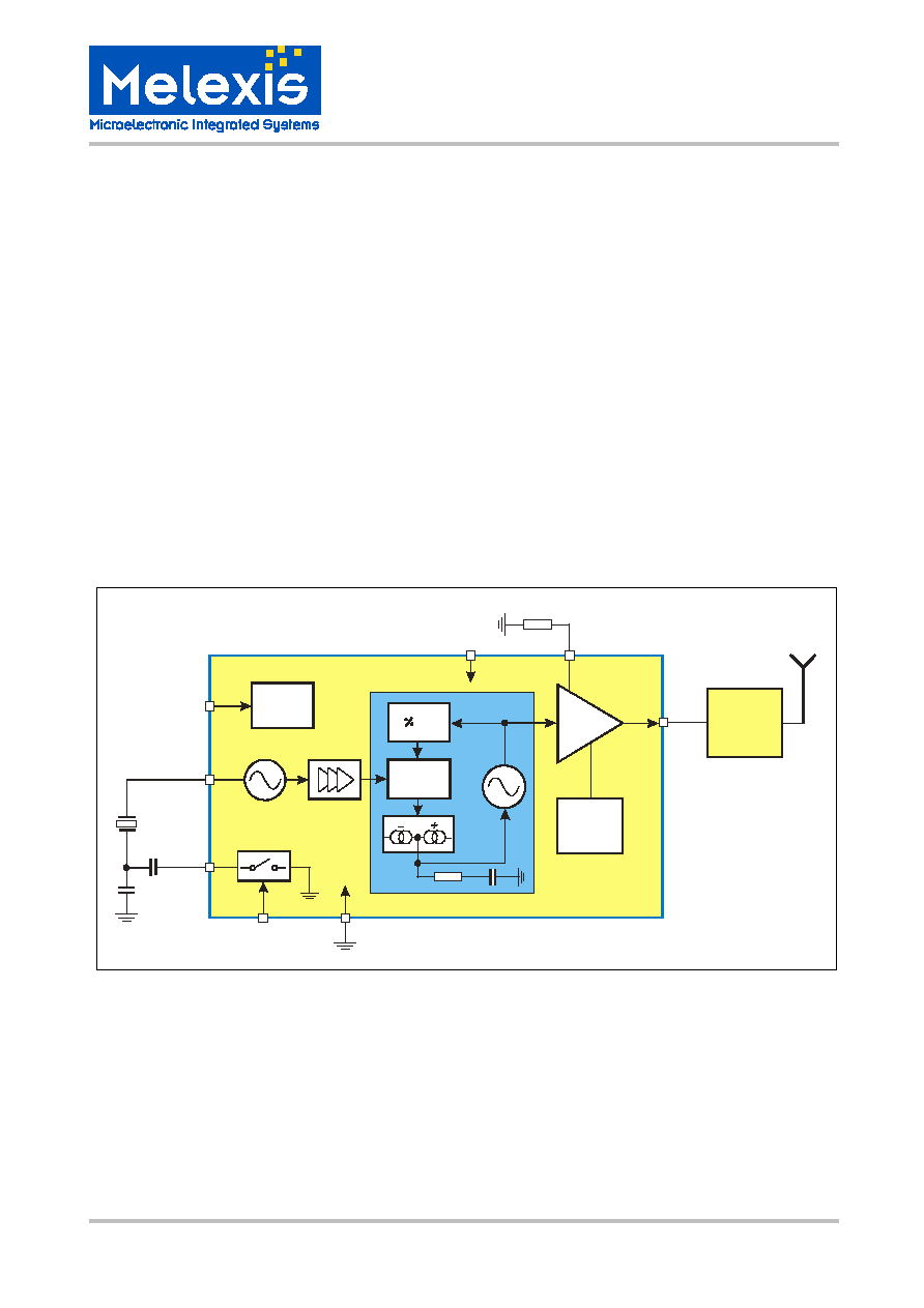
Theory of Operation
1.1 General
As depicted in Fig.1, the TH72031 transmitter consists of a fully integrated voltage-controlled oscillator
(VCO), a divide-by-32 divider (div32), a phase-frequency detector (PFD) and a charge pump (CP). An
internal loop filter determines the dynamic behavior of the PLL and suppresses reference spurious signals. A
Colpitts crystal oscillator (XOSC) is used as the reference oscillator of a phase-locked loop (PLL)
synthesizer. The VCO's output signal feeds the power amplifier (PA). The RF signal power P
out
can be
adjusted in four steps from P
out
= ≠12 dBm to +8.5 dBm, either by changing the value of resistor RPS
or by
varying the voltage V
PS
at pin PSEL. The open-collector output (OUT) can be used either to directly drive a
loop antenna or to be matched to a 50Ohm load. Bandgap biasing ensures stable operation of the IC at a
power supply range of 1.9 V to 5.5 V.
1.2 Block
Diagram
Fig. 1: Block diagram with external components
CX1
FSKDTA
antenna
matching
network
VEE
XOSC
low
voltage
detector
PA
XBUF
VCO
PLL
CP
PFD
32
OUT
PSEL
RPS
FSKSW
ROI
XTAL
CX2
8
1
7
5
3
2
mode
control
ENTX
4
6
VCC
TH72031
868/915MHz
FSK Transmitter
3901072031
Page 4 of 14
Data Sheet
Rev. 004
Feb./03
PR
ELI
MIN
AR
Y
2
Functional Description
2.1 Crystal
Oscillator
A Colpitts crystal oscillator with integrated functional capacitors is used as the reference oscillator for the PLL
synthesizer. The equivalent input capacitance CRO offered by the crystal oscillator input pin ROI is about
18pF. The crystal oscillator is provided with an amplitude control loop in order to have a very stable
frequency over the specified supply voltage and temperature range in combination with a short start-up time.
2.2 FSK
Modulation
FSK modulation can be achieved by pulling the
crystal oscillator frequency. A CMOS-
compatible data stream applied at the pin
FSKDTA digitally modulates the XOSC via an
integrated NMOS switch. Two external pulling
capacitors CX1 and CX2 allow the FSK
deviation
f and the center frequency f
c
to be
adjusted independently. At FSKDTA = 0, CX2 is
connected in parallel to CX1 leading to the low-
frequency component of the FSK spectrum
(f
min
); while at FSKDTA = 1, CX2 is deactivated
and the XOSC is set to its high frequency f
max
.
An external reference signal can be directly AC-
coupled to the reference oscillator input pin
ROI. Then the transmitter is used without a
crystal. Now the reference signal sets the
carrier frequency and may also contain the FSK
(or FM) modulation.
Fig. 2: Crystal pulling circuitry
FSKDTA
Description
0
f
min
= f
c
-
f (FSK switch is closed)
1
f
max
= f
c
+
f (FSK switch is open)
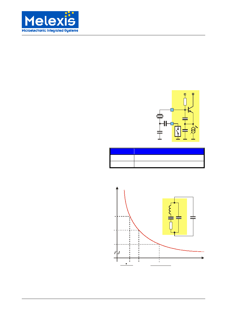
2.3 Crystal
Pulling
A crystal is tuned by the manufacturer to the
required oscillation frequency f
0
at a given load
capacitance CL and within the specified
calibration tolerance. The only way to pull the
oscillation frequency is to vary the effective load
capacitance CL
eff
seen by the crystal.
Figure 3 shows the oscillation frequency of a
crystal as a function of the effective load
capacitance. This capacitance changes in
accordance with the logic level of FSKDTA
around the specified load capacitance. The
figure illustrates the relationship between the
external pulling capacitors and the frequency
deviation.
It can also be seen that the pulling sensitivity
increases with the reduction of CL. Therefore,
applications with a high frequency deviation
require a low load capacitance. For narrow
band FSK applications, a higher load
capacitance could be chosen in order to reduce
the frequency drift caused by the tolerances of
the chip and the external pulling capacitors.
Fig. 3: Crystal pulling characteristic
CX2
VCC
XTAL
CX1
ROI
FSKSW
VEE
f
min
f
o
f
f
max
eff
CL
eff
CL
R1
C1
C0
L1
XTAL
CL
CX1 CRO
CX1+CRO
(CX1+CX2) CRO
CX1+CX2+CRO
TH72031
868/915MHz
FSK Transmitter
3901072031
Page 5 of 14
Data Sheet
Rev. 004
Feb./03
PR
ELI
MIN
AR
Y
2.4 Output Power Selection
The transmitter is provided with an output power selection feature. There are four predefined output power
steps and one off-step accessible via the power selection pin PSEL. A digital power step adjustment was
chosen because of its high accuracy and stability. The number of steps and the step sizes as well as the
corresponding power levels are selected to cover a wide spectrum of different applications.
The implementation of the output power control
logic is shown in figure 4. There are two
matched current sources with an amount of
about 8 µA. One current source is directly
applied to the PSEL pin. The other current
source is used for the generation of reference
voltages with a resistor ladder. These reference
voltages are defining the thresholds between
the power steps. The four comparators deliver
thermometer-coded control signals depending
on the voltage level at the pin PSEL. In order to
have a certain amount of ripple tolerance in a
noisy environment the comparators are
provided with a little hysteresis of about 20 mV.
With these control signals, weighted current
sources of the power amplifier are switched on
or off to set the desired output power level
(Digitally Controlled Current Source). The
LOCK signal and the output of the low voltage
detector are gating this current source.
Fig. 4: Block diagram of output power control circuitry
There are two ways to select the desired output power step. First by applying a DC voltage at the pin PSEL,
then this voltage directly selects the desired output power step. This kind of power selection can be used if
the transmission power must be changed during operation. For a fixed-power application a resistor can be
used which is connected from the PSEL pin to ground. The voltage drop across this resistor selects the
desired output power level. For fixed-power applications at the highest power step this resistor can be
omitted. The pin PSEL is in a high impedance state during the "TX standby" mode.
2.5 Lock
Detection
The lock detection circuitry turns on the power amplifier only after PLL lock. This prevents from unwanted
emission of the transmitter if the PLL is unlocked.
2.6 Low Voltage Detection
The supply voltage is sensed by a low voltage detect circuitry. The power amplifier is turned off if the supply
voltage drops below a value of about 1.85 V. This is done in order to prevent unwanted emission of the
transmitter if the supply voltage is too low.
&
&
&
PSEL
&
&
RPS
OUT