 | –≠–ª–µ–∫—Ç—Ä–æ–Ω–Ω—ã–π –∫–æ–º–ø–æ–Ω–µ–Ω—Ç: TH8061 | –°–∫–∞—á–∞—Ç—å:  PDF PDF  ZIP ZIP |

TH8061
Voltage Regulator with integrated LIN Transceiver
TH8061
≠
Datasheet
Page
1
of
30
3901008061
January 2003
Rev 005
Features
Features
Features
Features
o
Operating voltage V
SUP
= 5.5 to 18 V
o
Very low standby current consumption < 110 µA in normal mode (< 50 µA in sleep mode)
o
LIN-Bus Transceiver:
-
PNP-bipolar transistor driver
-
Slew rate control and wave shaping for best EMC behaviour
-
BUS input voltage -24V to 30V (independently of V
SUP
)
-
Possibility of wake up via LIN bus
-
Baud rate up to 20 kBaud
-
Compatible to LIN Specification 1.3
o
Wake-up by LIN BUS traffic and start-up capable independent of EN voltage level
o
Linear low drop voltage regulator:
-
Output voltage 5V± 1%
-
Output current max. 50mA
-
Output current limitation
-
Overtemperature shutdown
o
Reset time 100ms and reset threshold voltage 4.65V
o
CMOS compatible interface to microcontroller
o
Load dump protected (40V)
o
Resistant against transient pulses according to ISO 7637 at pin VSUP, BUS and EN
Ordering Information
Part
No.
Temperature
Range
Package
TH8061
K (-40 to 125 ∞C)
DC (SOIC8, 150mil)
General Description
General Description
General Description
General Description
The mini-ReLIN TH8061 is the low cost variant of our ReLIN-IC TH8060. It consist a low drop voltage regulator 5V/50mA
and a LIN bus transceiver. The LIN transceiver is suitable for LIN bus systems conform to "LIN-Protocol Specification"
rev.1.3.
The combination of voltage regulator and bus transceiver make it possible to develop simple, but powerful and cheap
slave nodes in LIN Bus systems.

TH8061
Voltage Regulator with integrated LIN Transceiver
TH8061
≠
Datasheet
Page
2
of
30
3901008061
January 2003
Rev 005
Contents
1.
Functional Diagram................................................................................................................................ 4
2.
Electrical Specification .......................................................................................................................... 5
2.1
Operating Conditions ........................................................................................................................ 5
2.2
Absolute Maximum Ratings.............................................................................................................. 5
2.3
Static Characteristics ........................................................................................................................ 6
2.4
Dynamic Characteristics ................................................................................................................... 8
2.5
Timing Diagrams............................................................................................................................... 9
2.6
Test Circuit for Dynamic and Static Characteristics ....................................................................... 10
3.
Functional Description ........................................................................................................................ 12
3.1
Operating Modes ............................................................................................................................ 12
3.2
LIN BUS Transceiver ...................................................................................................................... 12
3.3
Linear Regulator ............................................................................................................................. 14
3.4
RESET ............................................................................................................................................ 14
3.5
Initialization ..................................................................................................................................... 15
3.6
Mode Input EN................................................................................................................................ 15
3.7
Wake-Up......................................................................................................................................... 15
3.8
Overtemperature Shut Down.......................................................................................................... 15
4.
Application Hints.................................................................................................................................. 16
4.1
LIN System Parameter ................................................................................................................... 16
4.1.1.
Bus loading requirements ...................................................................................................... 16
4.1.2.
Recommendations for system design.................................................................................... 17
4.2
Min/max slope time calculation....................................................................................................... 18
4.3
Power Dissipation and operating range.......................................................................................... 19
4.4
Regulator circuitry........................................................................................................................... 21
4.5
Application circuitry......................................................................................................................... 21
4.6
EMI Supressing .............................................................................................................................. 21
4.7
Connection to Flash-MCU .............................................................................................................. 23
5.
Operating during Disturbance ............................................................................................................ 24
5.1
Operating without VSUP or GND ................................................................................................... 24
5.2
Short Circuit BUS against VBAT .................................................................................................... 24
5.3
Short Circuit BUS against GND...................................................................................................... 24
5.4
Short Circuit TxD against GND....................................................................................................... 24
5.5
TxD open ........................................................................................................................................ 24
5.6
Short Circuit VCC against GND...................................................................................................... 24
5.7
Overload of VCC............................................................................................................................. 24
5.8
Undervoltage VSUP, VCC.............................................................................................................. 24
5.9
Short circuit RxD, RESET against GND or VCC ............................................................................ 24
6.
PIN Description..................................................................................................................................... 25
7.
Mechanical Specification .................................................................................................................... 26
8.
ESD/EMC Remarks............................................................................................................................... 27
8.1
General Remarks............................................................................................................................ 27
8.2
ESD-Test ........................................................................................................................................ 27
8.3
EMC ................................................................................................................................................ 27
9.
Revision History ................................................................................................................................... 28
10.
Reliability Information.......................................................................................................................... 29
11.
Disclaimer ............................................................................................................................................. 29

TH8061
Voltage Regulator with integrated LIN Transceiver
TH8061
≠
Datasheet
Page
3
of
30
3901008061
January 2003
Rev 005
List of Figures
List of Figures
List of Figures
List of Figures
Figure 1- Block diagram .................................................................................................................................. 4
Figure 2 - Timing diagram for propagation delay............................................................................................ 9
Figure 3 - Timing diagram for slope times ...................................................................................................... 9
Figure 4 - Test circuit for delay time and slope control ................................................................................... 10
Figure 5 - Test circuit for supply current I
Snl
.................................................................................................... 10
Figure 6 - Test circuit for bus voltage "recessiv" V
BUSR
................................................................................... 10
Figure 7 - Test circuit for bus voltage "recessiv" V
BUSR
................................................................................... 11
Figure 8 - Test circuit for bus current "recessiv" I
BUSR
..................................................................................... 11
Figure 9 - Receive mode impulse diagram ..................................................................................................... 13
Figure 10 - Characteristic of current limitation VCC = f(I
VCC
).......................................................................... 14
Figure 11 - Reset behaviour ........................................................................................................................... 14
Figure 12 - Power dissipation LIN transceiver @ 20kbit................................................................................. 19
Figure 13 - Save operating area ..................................................................................................................... 20
Figure 14 - Application circuit (slave node)..................................................................................................... 21
Figure 15 - Application circuit for LIN subbus with TH8061 as slave node .................................................... 22
Figure 16 - Connection of RxD to MCU for flash programming...................................................................... 23

TH8061
Voltage Regulator with integrated LIN Transceiver
TH8061
≠
Datasheet
Page
4
of
30
3901008061
January 2003
Rev 005
1.
1.
1.
1. Functional Diagram
Functional Diagram
Functional Diagram
Functional Diagram
Wake-up
Control
Osc
VSUP
EN
VCC
Reset
Generator
Mode
Control
Aux.
Supply
Bandgap
Adjustment
current
limitation
control
amplifier
Temp.
Protection
Reset
Timer
TSHD
VBG
MR
VSS
RESET
VCC
4.65 V
BUS
30k
Rec-Filter
Wake-
Filter
RxD
Receiver
VSUP
Driver
control
TSHD
VCC
TxD
MR
Filter
VCC
Figure 1- Block diagram
TH8061
Voltage Regulator with integrated LIN Transceiver
TH8061
≠
Datasheet
Page
5
of
30
3901008061
January 2003
Rev 005
2.
2.
2.
2. Electrical Specification
Electrical Specification
Electrical Specification
Electrical Specification
All voltages are referenced to ground (GND). Positive currents flow into the IC.
The absolute maximum ratings (in accordance with IEC 134) given in the table below are limiting values that
do not lead to a permanent damage of the device but exceeding any of these limits may do so. Long term
exposure to limiting values may affect the reliability of the device. Correct operating of the device can't be
guaranteed if any of these limits are exceeded.
2.1 Operating
Conditions
Parameter
Symbol
Min
Max
Unit
Supply voltage
V
SUP
5.25
18
V
Output voltage
V
CC
4.95
5.05
V
Operating ambient temperature
T
A
-40
+125
∞C
Junction temperature
[1]
T
Jc
+150
∞C
2.2 Absolute Maximum Ratings
Parameter
Symbol
Condition
Min
Max
Unit
-1.0
18
T
60 s
-
30
Supply voltage at VSUP
[1]
V
SUP
T
500 ms
-
40
V
-24
30
Input voltage at pin BUS
[1]
V
BUS
T
500 ms
-
40
V
Difference VSUP-VCC
V
SUP
-V
CC
-0.3
40
V
Input voltage at pin EN
V
INEN
-0.3
V
SUP
+0.3
V
Input voltage at pin TxD, RxD, RESET
V
IN
-0.3
V
CC
+0.3
V
Input current at pin EN, TxD, RxD, RESET
I
IN
-25
25
mA
Input current for short circuit of pin VSUP and VCC
I
INSH
-500
500
mA
ESD Capability on pin BUS
ESD
BUSHB
Human body Modell, 100pF
via 1.5k
-2 2
kV
ESD Capability on all other pins
ESD
HB
Human body Modell, 100pF
via 1.5k
-2 2
kV
Power dissipation
P
0
Internal limited
[2]
Thermal resistance from junction to ambient(SOIC8)
R
THJA
160
K/W
Junction temperature
[3]
T
J
150
∞C
Storage temperature
T
STG
-55
150
∞C
[1]
The current and voltage values are valid independent from each other.
[2]
See chapter 4.3 Power Dissipation and operating range
[3]
See chapter 3.8 Overtemperature Shut Down and 4.3 Power Dissipation and operating range

TH8061
Voltage Regulator with integrated LIN Transceiver
TH8061
≠
Datasheet
Page
6
of
30
3901008061
January 2003
Rev 005
2.3 Static
Characteristics
Unless otherwise specified all values in the following tables are valid for V
SUP
= 5.25...18V and
T
AMB
= -40...125
o
C. All voltages are referenced to ground (GND), positive currents are flow into the IC.
Parameter
Symbol
Condition
Min
Typ
Max
Unit
VSUP
Operating voltage
V
SUP
5.25 12 18 V
Supply current, VCC ,,noload"
[3]
I
Snl
V
EN
= V
SUP
= 12V,
V
BUS
> V
SUP
-0.5V,
Pins 4 to 8 open
110
µA
Supply current, ,,sleep mode"
I
Ssleep
V
SUP
= 12V,
V
EN
= 0V,
V
BUS
> V
SUP
-0.5V
35
50
µA
VCC
V
CCn
5.5V
V
SUP
18V
T
A
= 25∞C
4.95
5.0
5.05
V
V
CCt
5.5V
V
SUP
18V
4.90
5.0
5.10
V
V
CCh
V
SUP
> 18V
4.95
5.0
5.25
V
Output voltage VCC
V
CCI
3.3 V< V
SUP
< 5.5 V
V
SUP
-V
D
5.1
V
I
VCC
= 20mA
150
mV
Drop-out voltage
[4]
V
D
I
VCC
= 50mA
500
mV
Output current VCC
I
VCC
V
SUP
3.0V
50
mA
Current limitation VCC
I
LVCC
V
SUP
> 0V
150
mA
Load capacity
C
load
1 ESR 7
2
µF
Reset threshold
V
RES
refered to V
CC
, V
SUP
> 4.6V
4.5
4.65
4.8
V
Power-on-reset threshold
[1]
V
POR
3.0
3.15
3.3
V
Enable Input EN
Input voltage low
V
ENL
-0.3
1.6
V
Input voltage high
V
ENH
2.5
V
SUP
+0.3
V
Hysteresis
[1]
V
ENHYS
100
mV
V
EN
> V
ENH
1.8
4.0
7.5
µA
Pull-down current EN
I
pdEN
V
EN
< V
ENL
70
100
130
µA
RESET Output
I
OUT
= 1 mA, V
SUP
> 5.5 V
0.8
V
Output voltage low
V
OL
10 k
RESET to VCC
V
SUP
= V
CC
= 0.8 V
0.2
V
Pull-up current
I
pu
-500
-375
-250
µA

TH8061
Voltage Regulator with integrated LIN Transceiver
TH8061
≠
Datasheet
Page
7
of
30
3901008061
January 2003
Rev 005
Parameter
Symbol
Condition
Min
Typ
Max
Unit
LIN BUS Interface
Receive threshold
V
thr_rec
,
V
thr_dom
0.4* V
SUP
0.6*
V
SUP
Center point of receive threshold
V
thr_cnt
= (V
thr_rec
+V
thr_dom
)/2
V
thr_cnt
0.475*
V
SUP
0.5*
V
SUP
0.525*
V
SUP
Hysteresis of receive threshold
V
thr_hys
= V
thr_rec
-V
thr_dom
V
thr_hys
7.3 V
V
SUP
18 V
0.12*
V
SUP
0.135*
V
SUP
0.15*
V
SUP
V
Input current BUS (recessive)
[3]
I
INBUSR
8
V
BUS
18 V,
V
SUP
= V
BUS
- 0.7V, TxD = 5V
20
µA
Input current BUS (recessive)
-I
INBUSR
V
SUP
= 0V, V
BUS
- 12V
-1
mA
Pull up resistor bus
R
BUSpu
20
30
47
k
Output voltage BUS (dominant)
[3]
V
BUSdom
7.3
V
SUP
18 V,
TxD = 0V, R
L
= 500
1.2
V
Output voltage BUS (recessive)
[2] [3]
V
BUSrec
7.3
V
SUP
18 V, TxD = 5V
0.8*V
SUP
V
Current limitation BUS
I
LIM
V
BUS
> 2.5V, TxD = 0V
40
120
mA
Input TxD
Pull-up Strom TxD
I
pu
-500 -375 -250
µA
Input low level TxD
V
IL
0.25
V
CC
Input high level TxD
V
IH
0.75
V
CC
Output RxD
Output voltage Low RxD
V
OL
I
OUT
= 1 mA
0.8
V
Output voltage High RxD
V
OH
I
OUT
= -1 mA
V
CC
- 0.3
V
Thermal Protection
Thermal shutdown
[1]
T
jshutdown
155
175
∞C
Thermal recovery
[1]
T
jrec
126
130
∞C
[1]
No production test, guaranteed by design and qualification
[2]
The recessive voltage at pin BUS don't should be less than 80% of voltage at KL30 V
BAT.
The voltage at V
SUP
results with
consideration of reverse diode V
SUP
= V
BAT
- 0,7V
[3]
See chapter 2.6 Test Circuit for Dynamic and Static Characteristics
[4]
The nominal V
CC
voltage is measured at V
SUP
=12V. If the V
CC
voltage is 100mV below its nominal value then the voltage drop is
V
D
= V
SUP
≠ V
CC
.

TH8061
Voltage Regulator with integrated LIN Transceiver
TH8061
≠
Datasheet
Page
8
of
30
3901008061
January 2003
Rev 005
2.4 Dynamic
Characteristics
8V
V
SUP
18V, -40∞C T
A
125∞C, unless otherwise specified
Parameter
Symbol
Condition
Min
Typ
Max
Unit
RESET
Reset time
t
Res
70
100
140
ms
Reset rising time
[1]
t
rr
3.0
6.5
10
µs
LIN BUS Interface
Transmit propagation delay
TxD -> BUS
[2]
[3]
t
dr_TXD
,
t
df_TXD
R
L
/C
L
at BUS
1k
/1nF
660
/6.8nF
500
/10nF
4
µs
Symmetry of propagation delay
BUS -> RxD
[2]
t
dsym_TXD
t
dr_TXD
- t
df_TXD
-2
2
µs
Receiver propagation delay
BUS -> RxD
[2]
[3]
t
dr_RXD
t
df_RXD
C
L(RXD)
= 50pF
6
µs
Symmetry of propagation delay
TxD -> BUS
[2]
t
dsym_RXD
t
dr_RXD
- t
df_RXD
-2
2
µs
Slew rate BUS rising edge
[1]
dV/dT
rise
20%
V
BUS
80%
C
BUS
= 100 pF
1.0
2.0
2.5
V/
µs
Slew rate BUS falling edge
[1]
dV/dT
fall
20%
V
BUS
80%
100pF
C
BUS
10nF
-2.5
-2.0
-1.0
V/
µs
Slope time, transition from recessive to
dominant
[3] [4]
t
sdom
V
SUP
= 8 V
R
L
= 500
/ C
L
=10nF
12
µs
Slope time, transition from dominant to
recessive
[3] [5]
t
srec
V
SUP
= 8 V
R
L
= 500
/ C
L
=10nF
12
µs
Slope time symmetry
t
ssym
V
SUP
= 8 V
R
L
= 500
/ C
L
=10nF
T
ssym
= t
sdom
- t
srec
-7 1
µs
Slope time, transition from recessive to
dominant
[3] [4]
t
sdom
V
SUP
= 18 V
R
L
= 500
/ C
L
=10nF
18
µs
Slope time, transition from dominant to
recessive
[3] [5]
t
srec
V
SUP
= 18 V
R
L
= 500
/ C
L
=10nF
18
µs
Slope time symmetry
t
ssym
V
SUP
= 18 V
R
L
= 500
/ C
L
=10nF
T
ssym
= t
sdom
- t
srec
-5 5
µs
Debouncing time BUS
t
deb_BUS
1.5
2.8
4.0
µs
Wake-up time
t
Wake_BUS
25 60 120
µs
[1]
No production test, guaranteed by design and qualification
[2]
See chapter 2.5 Timing Diagrams timing diagram
[3]
See chapter 2.6 Test Circuit for Dynamic and Static Characteristics
[4] t
sdom
= (t
VBUS40%
- t
VBUS95%
) / 0.55
[5] t
sdom
= (t
VBUS60%
- t
VBUS5%
) / 0.55

TH8061
Voltage Regulator with integrated LIN Transceiver
TH8061
≠
Datasheet
Page
9
of
30
3901008061
January 2003
Rev 005
2.5 Timing
Diagrams
Figure 2 - Timing diagram for propagation delay
Figure 3 - Timing diagram for slope times

TH8061
Voltage Regulator with integrated LIN Transceiver
TH8061
≠
Datasheet
Page
10
of
30
3901008061
January 2003
Rev 005
2.6 Test Circuit for Dynamic and Static Characteristics
Figure 4 - Test circuit for delay time and slope control
Figure 5 - Test circuit for supply current I
Snl
Figure 6 - Test circuit for bus voltage "recessiv" V
BUSR

TH8061
Voltage Regulator with integrated LIN Transceiver
TH8061
≠
Datasheet
Page
11
of
30
3901008061
January 2003
Rev 005
Figure 7 - Test circuit for bus voltage "recessiv" V
BUSR
Figure 8 - Test circuit for bus current "recessiv" I
BUSR

TH8061
Voltage Regulator with integrated LIN Transceiver
TH8061
≠
Datasheet
Page
12
of
30
3901008061
January 2003
Rev 005
3.
3.
3.
3. Functional Description
Functional Description
Functional Description
Functional Description
The TH8061 consist a low drop voltage regulator 5V/50mA and a LIN Bus transceiver, which is a bi-
directional bus interface for data transfer between LIN bus and the LIN protocol controller.
Additional integrated is a RESET output with a reset delay of 100ms and a fixed threshold of 4.65V.
3.1 Operating
Modes
Via the EN pin it is possible to switch the TH8061 into different operating modes:
Normal Mode
The whole TH8061 is active. Switching to normal mode can be done via the following actions:
-
Rising edge at EN (EN=high)
(local wake-up)
-
Activity on the LIN bus
(remote wake-up)
-
Power On Reset
Sleep Mode
The sleep mode is most current saving mode. With a falling edge on EN (EN=low) it is possible to switch to
this mode. The voltage regulator will be switched off and the LIN transceiver is in recessive state.
Switching into sleep mode can be done independent from the current transceiver state, that means if the
transmitter is in dominant state this state will be cancelled and it will be switched to recessive state.
Thermal Shutdown Mode
If the junction temperature T
J
is higher than 155∞C, the TH8061 will be switched into the thermal shutdown
mode. The impact of this mode is comparable with the sleep mode.
If T
J
falls below the thermal shutdown temperature (typ. 140∞C) the TH8061 will be switched to the previous
state.
3.2 LIN BUS Transceiver
The TH8061 is a bi-directional bus interface device for data transfer between LIN bus and the LIN protocol
controller.
The transceiver consist a pnp-driver (1.2V@40mA) with slew rate control, wave shaping and current
limitation and consists as well in the receiver a high voltage comparator followed by a debouncing unit.
Transmit Mode
During transmission the data at the pin TxD will be transferred to the BUS driver for generating a BUS signal.
To minimize the electromagnetic emission of the bus line, the BUS driver has an integrated slew rate control
and wave shaping unit.
Transmitting will be interrupted in the following cases:
- Sleep
mode
-
Thermal Shutdown active
-
Master Reset (V
CC
< 3.15V)
The recessive BUS level is generated from the integrated 30k pull up resistor in serial with a active diode
This diode prevent the reverse current of V
BUS
during differential voltage between VSUP and BUS
(V
BUS
>V
SUP
).
No additional termination resistor is necessary to use the TH8061 in LIN slave nodes. If this IC is used for
LIN master nodes it is necessary that the BUS pin is terminated via a external 1k
resistor in serial with a
diode to VBAT.

TH8061
Voltage Regulator with integrated LIN Transceiver
TH8061
≠
Datasheet
Page
13
of
30
3901008061
January 2003
Rev 005
Receive Mode
The data signals from the BUS pin will be transferred continuously to the pin RxD. Short spikes on the bus
signal are suppressed by the implemented debouncing circuit (
= 2.8µs).
Figure 9 - Receive mode impulse diagram
The receive threshold values V
thr_max
and V
thr_min
are symmetrical to the centre voltage of 0.5*V
SUP
with a
hysteresis of 0.135*V
SUP
. Including all tolerances the LIN specific receive threshold values of 0.4*V
SUP
and
0.6*V
SUP
will be secure observed.
Datarate
The TH8061 is a constant slew rate transceiver that means the bus driver works with a fixed slew rate
range of 1.0 V/µs
V/T 2.5V/µs. This principle secures a very good symmetry of the slope times
between recessive to dominant and dominant to recessive slopes within the LIN bus load range (C
BUS
, R
term
).
The TH8061 guarantees data rates up to 20kbit within the complete bus load range under worst case
conditions. The constant slew rate principle is very robust against voltage drops and can operate with RC-
oscillator systems with a clock tolerance up to ±2% between 2 nodes.
Input TxD
The 5V input TxD controls directly the BUS level:
TxD = low
->
BUS = low (dominant level)
TxD = high
->
BUS = high (recessive level)
The TxD pin has an internal pull up resistor connected to VCC. This secures that an open TxD pin generates
a recessive BUS level.
Output RxD
The received BUS signal will be output to the 5V RxD pin:
BUS
<
V
thr_cnt
≠ 0.5 * V
thr_hys
-> RxD
=
low
BUS
>
V
thr_cnt
+ 0.5 * V
thr_hys
->
RxD = high
This output is a push-pull driver between VCC and GND with a output current of 1mA.

TH8061
Voltage Regulator with integrated LIN Transceiver
TH8061
≠
Datasheet
Page
14
of
30
3901008061
January 2003
Rev 005
3.3 Linear
Regulator
The TH8061 has an integrated low drop linear regulator with a p-channel-MOSFET as driving transistor. This
regulator outputs a voltage of 5V ±2% and a current of
50mA within an input voltage range of
5.5V V
SUP
18V. The current limitation unit limits the output current for short circuits or over load to 100mA
respectively drop down the V
CC
voltage.
0
1
2
3
4
5
6
0
20
40
60
80
100
120
I
VCC
[mA]
Figure 10 - Characteristic of current limitation VCC = f(I
VCC
)
3.4 RESET
The RESET pin output the reset state of the TH8061. This output is switched from low to high if V
SUP
is
switched on and V
CC
>V
RES
after the time t
Res
.
Figure 11 - Reset behaviour
If the voltage V
CC
drop below V
RES
then the RESET output is switched from high to low after the time t
rr
has been
reached. For this reason short breaks of the V
CC
voltage and uncontrolled reset generations will be inhibit.
The RESET output driver secures that the reset low level during decreasing of the V
CC
voltage will be secure
generated.

TH8061
Voltage Regulator with integrated LIN Transceiver
TH8061
≠
Datasheet
Page
15
of
30
3901008061
January 2003
Rev 005
3.5 Initialization
The initialization is started if the power supply is switched on respectively every start of the voltage regulator
after switching off.
VSUP- Power ON
The TH8061 start with the normal mode if V
SUP
is switched on. The internal circuitry on VCC as well as the
internal help supply starts the initialisation with power-on-reset. The voltage regulator is switched on.
If V
CC
>V
POR
the bus-interface will be activated.
If the V
CC
voltage level is higher than V
Res
, the reset time t
Res
= 100ms is started. After t
Res
the RESET output
switches from low to high (see Figure 11).
The initialisation procedure at power on is started independent from the EN state.
Start of Linear Regulator
The initialization is only being done for the VCC circuitry parts. This procedure begins with leaving the master
reset state (V
CC
> V
POR
) and runs in the same manner as the VSUP-Power-On.
3.6 Mode Input EN
The TH8061 is switched into the sleep mode with a falling edge and into normal mode with a rising edge at
the EN pin. The normal mode will be kept as long as EN = high.
The deactivation of TH8061 with a falling edge at EN can be done independent from the state of the bus-
transceiver.
The EN input is internal pulled down so that it is secured if this pin is not connected a low level will be
generated. In the high state the pull down current will be switched off to reduce the quiescent current.
3.7 Wake-Up
If the regulator is put in standby mode it can be wake up with the BUS interface. Every pulse on the BUS
(high pulse or low pulse) with a pulse width of min. 45
µs switches on the regulator.
After the BUS has wake up the regulator, it can only be switched off with a high level followed by a low level
on the EN pin.
3.8 Overtemperature Shut Down
If the Junction temperature is 150∫C < T
j
< 170∫C the over temperature recognition will be active and the
regulator voltage will be switched off. The V
CC
voltage drops down, the reset state is entered and the bus-
transceiver is switched off (recessive state).
After T
j
fall below 140∫C the TH8061 will be initialized (see Figure 11), independent from the voltage levels
on EN and BUS. Within the thermal shutdown mode the transceiver can't switched to the normal mode
neither with local nor with remote wake-up.
The function of the TH8061 is possible between T
Amax
(125∞C) and the switch off temperature, but small
parameter differences can appear.
After over temperature switch off the IC behave as described in chapter 3.4 RESET.

TH8061
Voltage Regulator with integrated LIN Transceiver
TH8061
≠
Datasheet
Page
16
of
30
3901008061
January 2003
Rev 005
4.
4.
4.
4. Application Hints
Application Hints
Application Hints
Application Hints
4.1
LIN System Parameter
4.1.1. Bus loading requirements
Parameter
Symbol
Min
Typ
Max
Unit
Operating voltage range
V
BAT
8
18
V
Voltage drop of reverse protection diode
V
Drop_rev
0.4 0.7 1
V
Voltage drop at the serial diode in pull up path
V
SerDiode
0.4 0.7 1
V
Battery shift voltage
V
Shift_BAT
0
0.1
V
BAT
Ground shift voltage
V
Shift_GND
0
0.1 V
BAT
Master termination resistor
R
master
900 1000
1100
Slave termination resistor
R
slave
20 30 60 k
Number of system nodes
N
2
16
Total length of bus line
LEN
BUS
40 m
Line capacitance
C
LINE
100
150
pF/m
Capacitance of master node
C
Master
220 pF
Capacitance of slave node
C
Slave
220
250
pF
Total capacitance of the bus including slave and
master capacitance
C
BUS
0.47 4 10 nF
Network Total Resistance
R
Network
500
862
Time constant of overall system
1 5
µs
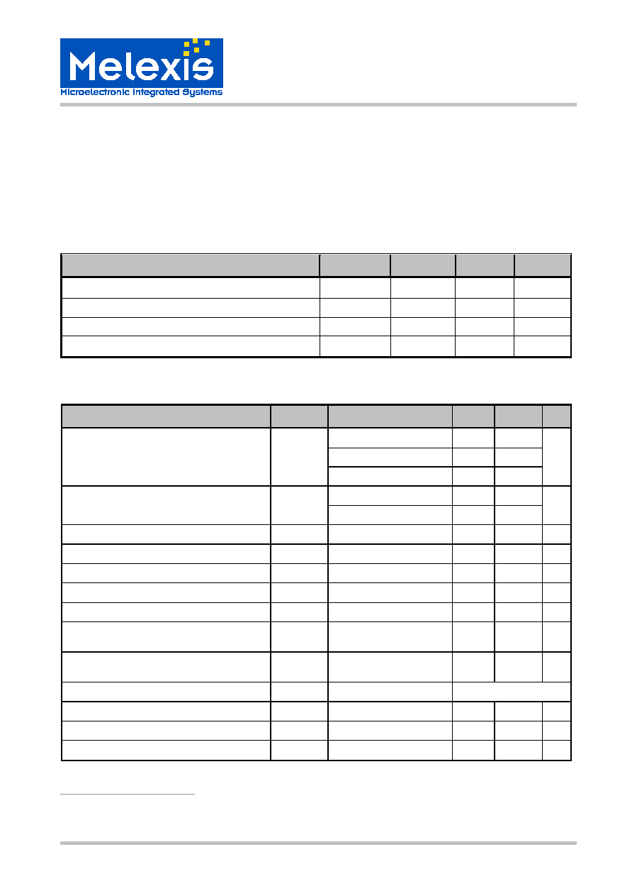
Table 1 - Bus loading requirements

TH8061
Voltage Regulator with integrated LIN Transceiver
TH8061
≠
Datasheet
Page
17
of
30
3901008061
January 2003
Rev 005
4.1.2. Recommendations for system design
The goal of the LIN physical layer standard is to be universal valid definition of the LIN system for plug &play
solutions in LIN networks up to 20kbd bus speed.
In case of small and medium LIN networks no problems occurring. It's recommended to adjust the total
network capacitance to at least 4nF for good EMC and EMI behavior. This can be done by adapting only the
master node capacitance. The slave node capacitance should have a unit load of typically 220pF for good
EMC/EMI behavior.
In large networks with long bus lines and the maximum number of nodes some system parameters can
exceed the defined limits and an intervention of the LIN system designer is required.
The whole capacitance of a slave node is not only the unit load capacitor itself. Additionally there is a
capacitance of wires and connectors and the internal capacitance of the LIN transmitter. This internal
capacitance is strongly dependent from the technology of the IC manufacturer and should be in the range of
30 to 150pF. If the bus lines have a total length of nearly 40m, the total bus capacitance can exceed 10nF.
A second reason for exceeding these limits is the tolerance of the integrated slave termination resistor. If
most of the slave nodes have a slave termination resistance near by the allowed maximum of 60k
, the total
network resistance is more than 700
. Even if the total network capacitance is below or equal to the
maximum specified value of 10nF, the network time constant is higher than 7
µs!
This problem can be removed only by adapting the master termination resistor to realize the required
maximum network time constant of 5
µs.
The LIN output driver of the TH8061 provides a higher driving capability than necessary within the LIN
standard (40mA @ 1.2V). With this driver stage the system designer have more degrees of freedom in case
of maximum LIN networks with a total network capacitance of more than 10nF. The total network resistance
can be decreased to:
R
tl_min
= (V
Bat_max
≠ V
BUSdom
) / I
BUS_max
= (18V ≠1.2V) / 40mA = 420
Note:
The adaptation of the network time constant is necessary in large networks (Master resistance)and also in
small networks (master capacitance).
The intervention in the LIN network has only to be done in the master ECU! The limits of the system have to
be known by the system designer and shouldn't have any influence to the LIN physical layer.
The TH8061 meets the requirements for implementation in RC-based slave nodes (oscillator tolerance <2%
at baudrate 20Kbit/s )under all worst case conditions in V
BAT
- or ground shift, operating voltage and load
conditions, and independent from the method of reverse polarity protection .
TH8061
Voltage Regulator with integrated LIN Transceiver
TH8061
≠
Datasheet
Page
18
of
30
3901008061
January 2003
Rev 005
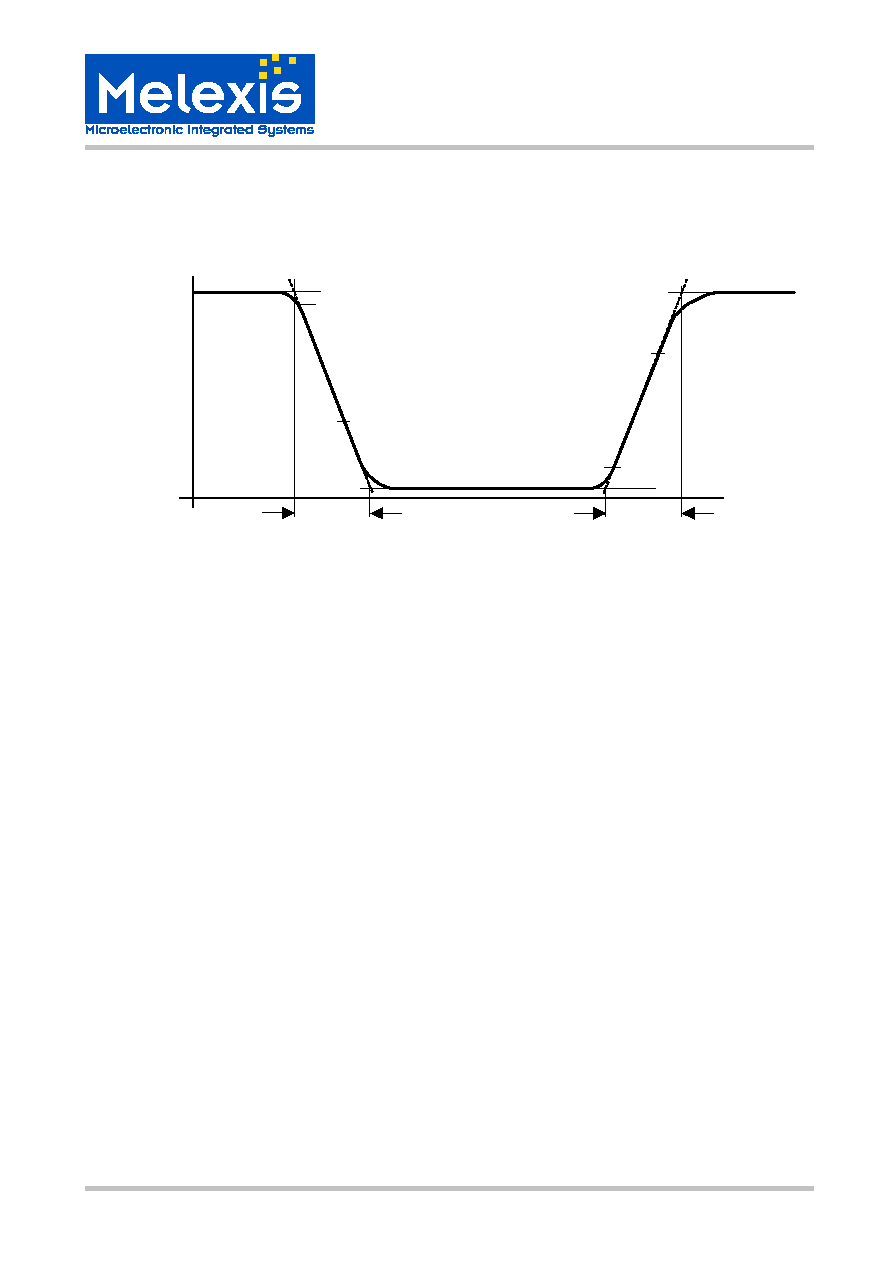
4.2 Min/max slope time calculation
BUS
V
BUS
95%
40%
t
sdom
5%
60%
100%
0%
t
srec
V
dom
Figure 12 - Slope time calculation
The slew rate of the bus voltage is measured between 40% and 60% of the output voltage swing (linear
region). The output voltage swing is the difference between dominant and recessive bus voltage.
dV/dt = 0.2*V
swing
/ (t
40%
- t
60%
)
The slope time is the extension of the slew rate tangent until the upper and lower voltage swing limits:
t
slope
= 5 * (t
40%
- t
60%
)
The slope time of the recessive to dominant edge is directly determined by the slew rate control of the
transmitter:
t
slope
= V
swing
/ dV/dt
The dominant to recessive edge is influenced from the network time constant and the slew rate control,
because it's a passive edge. In case of low battery voltages and high bus loads the rising edge is only
determined by the network. If the rising edge slew rate exceeds the value of the dominant one, the slew rate
control determines the rising edge.

TH8061
Voltage Regulator with integrated LIN Transceiver
TH8061
≠
Datasheet
Page
19
of
30
3901008061
January 2003
Rev 005
4.3 Power Dissipation and operating range
The max power dissipation depends on the thermal resistance of the package and the PCB, the temperature
difference between Junction and Ambient as well as the airflow.
The power dissipation can be calculated with:
P
D
= (V
SUP
≠ V
CC
) * I
VCC
+ P
D_TX
The power dissipation of the transmitter P
D_TX
depends on the transceiver configuration and its parameters
as well as on the bus voltage V
BUS
=V
BAT
-V
D
, the resulting termination resistance R
L
, the capacitive bus load
C
L
and the bit rate. Figure 13 shows the dependence of power dissipation of the transmitter as function of
V
SUP
. The conditions for calculation the power dissipation was: R
L
=500
, C
L
=10nF, Bitrate=20kbit and duty
cycle on TxD of 50%
Figure 13 - Power dissipation LIN transceiver @ 20kbit
The permitted package power dissipation can be calculated:
A
THJ
A
j
max
D
R
T
T
P
-
-
=
If we consider that P
D_TX_max
= f(V
SUP
) it can be calculated the max output current I
VCC
on V
CC
:
VCC
VSUP
P
R
T
T
I
VSUP
@
max
_
TX
_
D
A
THJ
A
j
CCmax
V
-
-
-
=
-
T
j
-T
A
is the temperature difference between junction and ambient and R
th
is the thermal resistance of the
package. The thermal energy is transferred via the package and the pins to the ambient. This transfer can be
improved with additional ground areas on the PCB as well as ground areas under the IC.

TH8061
Voltage Regulator with integrated LIN Transceiver
TH8061
≠
Datasheet
Page
20
of
30
3901008061
January 2003
Rev 005
Figure 14 - Save operating area
The linear regulator of the TH8061 operates with input voltages up to 18V and can output a current of 50mA.
The maximum power dissipation limits the maximum output current at high input voltages and high ambient
temperatures. The output current of 50mA at an ambient temperature of T
A
= 125∞C is only possible with
small voltage differences between V
SUP
and V
CC
. See Figure 14 for save operating areas for different
ambient and junction temperatures.

TH8061
Voltage Regulator with integrated LIN Transceiver
TH8061
≠
Datasheet
Page
21
of
30
3901008061
January 2003
Rev 005
4.4 Regulator
circuitry
Pin VCC
The linear regulator needs a minimum load capacity of 2µF connected to V
CC
for stable operating within the
whole operating area.
The choice of type and dimension of the load capacity must be done from the application point of view (e.g.
Tantal 10µF). Essential parameters are the switch on time of the VCC and the load regulation.
Small capacity values don't should combined with small ESR values to avoid stability problems.
Pin VSUP
The capacity connected to the VSUP pin influences the regulation behaviour especially the line regulation
and load regulation.
Big capacity values improve the line regulation and in parallel with a ceramic capacitor it archives good
disturbance suppressing.
4.5 Application
circuitry
Figure 15 - Application circuit (slave node)
4.6 EMI
Supressing
To minimize the influence of EMI on the bus line a 220pF capacitor should be direct connected to the BUS
pin (see Figure 15). This EMI-Filter causes that the RF immissions into the IC from the BUS line have no
affect resp. will be limited.
The value of the filter capacity can be adjusted to the size of the LIN network. 220pF should be used for
bigger networks. Values from 333pF up to 1nF should be used for middle to small LIN networks. Finally the
size of the filter capacity influences the effectiveness of the EMI suppressing in observation of the maximum
LIN bus capacity of 10nF.
Alternatively to a pure C-filter it is also possible to use LC- or RC-filter. The dimension of C, L or R, L
depends on the corner frequency, the maximum LIN bus capacity (10nF) and the compliance with the DC-
and AC LIN bus parameters.

TH8061
Voltage Regulator with integrated LIN Transceiver
TH8061
≠
Datasheet
Page
22
of
30
3901008061
January 2003
Rev 005
Figure 16 - Application circuit for LIN subbus with TH8061 as slave node

TH8061
Voltage Regulator with integrated LIN Transceiver
TH8061
≠
Datasheet
Page
23
of
30
3901008061
January 2003
Rev 005
4.7 Connection to Flash-MCU
During programming of a flash MCU the TH8061 should be disconnected from the MCU. This can be done
via disconnecting the supply voltage of the TH8061 or via switch off with the EN pin. The reverse current
supply of the IC via the RxD pin if the connected MCU pin is used as normal signal input and programming
input must be inhibit via decoupling with a diode. In this case the MCU must be supplied via the
programming interface.
Figure 17 ≠ Example circuitry for connection of RxD to MCU for flash programming

TH8061
Voltage Regulator with integrated LIN Transceiver
TH8061
≠
Datasheet
Page
24
of
30
3901008061
January 2003
Rev 005
5.
5.
5.
5. Operating during Disturba
Operating during Disturba
Operating during Disturba
Operating during Disturbance
nce
nce
nce
5.1 Operating without VSUP or GND
The BUS pin is designed for voltages of GND-24V up to GND+30V and this inhibit that the absence of V
SUP
or GND connection influence or disturb the communication between other bus nodes. No reverse supply of
the IC can appear if without GND or VSUP connection the BUS pin is on VBAT level.
5.2 Short Circuit BUS against VBAT
The reaction of the IC depends on the send state of the transceiver:
-
Recessive
LIN bus is blocked, no influence to the TH8061
- Dominant
Current limitation, thermal shut down of TH8061 if power dissipation will make an
overrun of T
J
5.3 Short Circuit BUS against GND
LIN bus is blocked. No influence to the TH8061.
5.4 Short Circuit TxD against GND
The LIN transceiver is permanent in the dominant state that mean the whole LIN bus. This state can only be
detected from the LIN controller. In this case the controller must switch off the LIN node via the EN input of
the TH8061. A thermal shut down of TH8061 will appear if the power dissipation will make an overrun of T
J.
5.5 TxD
open
The internal pull up resistor forces the LIN node to the recessive state. The communication between the
other bus-nodes will not disturb.
5.6 Short Circuit VCC against GND
The VCC pin is protected via a current limitation. This state is comparable with the behaviour in the sleep
mode.
5.7 Overload of VCC
Thermal switch off
The power dissipation is increasing if the load current is between I
VCC_max
and I
LVCC
. If the max junction
temperature of 150∞C is reached the IC will be switched off. The voltage regulator will also be switched off
and a reset signal is forced.
Over current
If the current limitation is active the voltage on VCC drops down. If this voltage under-run the threshold V
RES
a reset will be forced.
5.8 Undervoltage
VSUP,
VCC
The reset unit secures the correct behaviour of the driver during undervoltage. The BUS pin generates the
recessive state if V
CC
< V
POR
. The inputs EN and TxD have pull-up or pull-down characteristics.
If V
POR
V
CC
4.5V the TxD signal is transmitted to the bus. The receive mode is also active.
5.9 Short circuit RxD, RESET against GND or VCC
Both outputs are short circuit proof to VCC and ground.

TH8061
Voltage Regulator with integrated LIN Transceiver
TH8061
≠
Datasheet
Page
25
of
30
3901008061
January 2003
Rev 005
6.
6.
6.
6. PIN Description
PIN Description
PIN Description
PIN Description
TH8061
1
EN
RESET
BUS
GND
RxD
TxD
8
7
6
5
4
2
3
VSUP
VCC
Pin
Name
IO-Typ
Description
1
VSUP
Supply voltage
2
EN
I
Enable Input voltage regulator, HV-pull-down-Input, High-active
3
GND
Ground
4
BUS
I/O
LIN bus line
5
RxD
O
Receive Output, 5V-push-pull
6
TxD
I
5V-Transmit Input, pull-up-Input
7
RESET
O
Reset 5V-output, active low
8
VCC
O
Regulator output 5V/50mA

TH8061
Voltage Regulator with integrated LIN Transceiver
TH8061
≠
Datasheet
Page
26
of
30
3901008061
January 2003
Rev 005
7.
7.
7.
7. Mechanic
Mechanic
Mechanic
Mechanical Specification
al Specification
al Specification
al Specification
Small Outline Integrated Circiut (SOIC), SOIC 8, 150 mil
A1
B
C
D
E
e
H
h
L
A
ZD
A2
All Dimension in mm, coplanarity < 0.1 mm
min
max
0.10
0.25
0.36
0.46
0.19
0.25
4.80
4.98
3.81
3.99
1.27
5.80
6.20
0.25
0.50
0.41
1.27
1.52
1.72
0∞
8∞
0.53
1.37
1.57
All Dimension in inch, coplanarity < 0.004"
min
max
0.004
0.0098
0.014
0.018
0.0075
0.0098
0.189
0.196
0.150
0.157
0.050 0.2284
0.244
0.0099
0.0198
0.016
0.050
0.060
0.068
0∞
8∞
0.021 0.054
0.062

TH8061
Voltage Regulator with integrated LIN Transceiver
TH8061
≠
Datasheet
Page
27
of
30
3901008061
January 2003
Rev 005
8.
8.
8.
8. ESD
ESD
ESD
ESD/EMC
/EMC
/EMC
/EMC Remarks
Remarks
Remarks
Remarks
8.1 General
Remarks
Electronic semiconductor products are sensitive to Electro Static Discharge (ESD).
Always observe Electro Static Discharge control procedures whenever handling semiconductor products.
8.2 ESD-Test
The TH8061 is tested according MIL883D (human body model).
8.3 EMC
The test on EMC impacts is done according to ISO 7637-1 for power supply pins and ISO 7637-3 for data-
and signal pins.
Power Supply pin VSUP
:
Testpulse Condition
Duration
1 t
1
= 5 s / U
S
= -100 V /
t
D
= 2 ms
5000 pulses
2 t
1
= 0.5 s / U
S
= 100 V / t
D
= 0.05 ms
5000 pulses
3a/b
U
S
= -150 V/ U
S
= 100 V
burst 100ns / 10 ms / 90 ms break
1h
5
R
i
= 0.5
, t
D
= 400 ms
t
r
= 0.1 ms / U
P
+U
S
= 40 V
10 pulses every 1min
Data- and signal pins EN, BUS
:
Testpulse Condition
Duration
1 t
1
= 5 s / U
S
= -100 V /
t
D
= 2 ms
1000 pulses
2 t
1
= 0.5 s / U
S
= 100 V / t
D
= 0.05 ms
1000 pulses
3a/b
U
S
= -150 V/ U
S
= 100 V
burst 100ns / 10 ms / 90 ms break
1000 burst

TH8061
Voltage Regulator with integrated LIN Transceiver
TH8061
≠
Datasheet
Page
28
of
30
3901008061
January 2003
Rev 005
9.
9.
9.
9. Revision History
Revision History
Revision History
Revision History
Version
Changes
Remark
Date
1.0
Preliminary Release
Sep. 2000
1.2a
First official release
Feb. 2001
002
-
General changes to new document layout
-
Improved features description
-
Added detailed block diagram
-
Changed LIN Bus static and dynamic parameters to be conform to LIN
specification 1.2 and future 1.3
-
Added static parameters for pin TxD and RxD
-
Add timing diagram for slope time
-
Improved functional description
-
Added chapter "Operating during Disturbance"
-
Added chapter "Application Hints"
-
Added chapter "ESD/EMC Remarks"
-
Added chapter "Reliability Information"
-
Added chapter "Disclaimer"
Complete rework of
datasheet
Aug. 2002
003
-
Added chapter "LIN System Parameters"
-
Added chapter "Min/max slope time calculation"
Sep.
2002
004
-
Added chapter "Revision History"
15.11.02
005
-
Add compatibility to LIN 1.3
13.01.03

TH8061
Voltage Regulator with integrated LIN Transceiver
TH8061
≠
Datasheet
Page
29
of
30
3901008061
January 2003
Rev 005
10.
10.
10.
10. Reliability Information
Reliability Information
Reliability Information
Reliability Information
Melexis devices are classified and qualified regarding suitability for infrared, vapor phase and wave soldering
with usual (63/37 SnPb-) solder (melting point at 183degC).
The following test methods are applied:
-
IPC/JEDEC J-STD-020A (issue April 1999)
-
Moisture/Reflow Sensitivity Classification For Nonhermetic Solid State Surface Mount Devices
-
CECC00802 (issue 1994)
- Standard Method For The Specification of Surface Mounting Components (SMDs) of Assessed
Quality
-
MIL 883 Method 2003 / JEDEC-STD-22 Test Method B102
- Solderability
For all soldering technologies deviating from above mentioned standard conditions (regarding peak
temperature, temperature gradient, temperature profile etc) additional classification and qualification tests
have to be agreed upon with Melexis.
The application of Wave Soldering for SMD's is allowed only after consulting Melexis regarding assurance of
adhesive strength between device and board.
For more information on manufacturability/solderability see quality page at our website:
http://www.melexis.com/
11.
11.
11.
11. Disclaimer
Disclaimer
Disclaimer
Disclaimer
Devices sold by Melexis are covered by the warranty and patent indemnification provisions appearing in its
Term of Sale. Melexis makes no warranty, express, statutory, implied, or by description regarding the
information set forth herein or regarding the freedom of the described devices from patent infringement.
Melexis reserves the right to change specifications and prices at any time and without notice. Therefore,
prior to designing this product into a system, it is necessary to check with Melexis for current information.
This product is intended for use in normal commercial applications. Applications requiring extended
temperature range, unusual environmental requirements, or high reliability applications, such as military,
medical life-support or life-sustaining equipment are specifically not recommended without additional
processing by Melexis for each application.
The information furnished by Melexis is believed to be correct and accurate. However, Melexis shall not be
liable to recipient or any third party for any damages, including but not limited to personal injury, property
damage, loss of profits, loss of use, interrupt of business or indirect, special incidental or consequential
damages, of any kind, in connection with or arising out of the furnishing, performance or use of the technical
data herein. No obligation or liability to recipient or any third party shall arise or flow out of Melexis' rendering
of technical or other services.
© 2002 Melexis NV. All rights reserved.

TH8061
Voltage Regulator with integrated LIN Transceiver
TH8061
≠
Datasheet
Page
30
of
30
3901008061
January 2003
Rev 005
Your notes
Your notes
Your notes
Your notes
For the latest version of this document. Go to our website at
www.melexis.com
Or for additional information contact Melexis Direct:
Europe and Japan:
All other locations:
Phone: +32 1367 0495
Phone: +1 603 223 2362
E-mail: sales_europe@melexis.com
E-mail: sales_usa@melexis.com
QS9000, VDA6.1 and ISO14001 Certified