 | –≠–ª–µ–∫—Ç—Ä–æ–Ω–Ω—ã–π –∫–æ–º–ø–æ–Ω–µ–Ω—Ç: 4X16E43V | –°–∫–∞—á–∞—Ç—å:  PDF PDF  ZIP ZIP |
1
FEATURES
OPTIONS
MARKING
∑ Operating Temperature Range
Commercial (0∞C to +70∞C)
None
Extended (-40∞C to +85∞C)
IT
NOTE: 1. The "#" symbol indicates signal is active LOW.
Part Number Example:
MEM4X16E43VTW-5
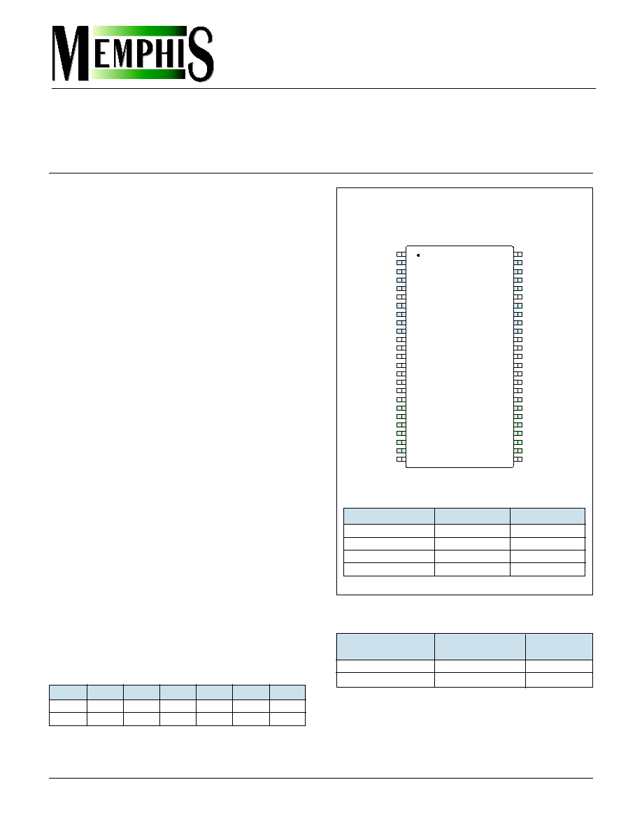
PIN ASSIGNMENT (Top View)
V
CC
DQ0
DQ1
DQ2
DQ3
V
CC
DQ4
DQ5
DQ6
DQ7
NC
V
CC
WE#
RAS#
NC
NC
NC
NC
A0
A1
A2
A3
A4
A5
V
CC
1
2
3
4
5
6
7
8
9
10
11
12
13
14
15
16
17
18
19
20
21
22
23
24
25
50
49
48
47
46
45
44
43
42
41
40
39
38
37
36
35
34
33
32
31
30
29
28
27
26
V
SS
DQ15
DQ14
DQ13
DQ12
V
SS
DQ11
DQ10
DQ9
DQ8
NC
V
SS
CASL#
CASH#
OE#
NC
NC
NC/
A12
A11
A10
A9
A8
A7
A6
V
SS
KEY TIMING PARAMETERS
SPEED
t
RC
t
RAC
t
PC
t
AA
t
CAC
t
CAS
-5
84ns
50ns
20ns
25ns
13ns
8ns
-6
104ns
60ns
25ns
30ns
15ns
10ns
50-Pin TSOP
4 MEG x 16 EDO DRAM PART NUMBERS
REFRESH
PART NUMBER ADDRESSING PACKAGE
4X16E43VTW-x 4 400-TSOP
4X16E83VTW-x 8 400-TSOP
x = speed
4X16E43V 4X16E83V
Configuration
4 Meg x 16
4 Meg x 16
Refresh
4K
8K
Row Address
4K (A0-A11)
8K (A0-A12)
Column Addressing
1K (A0-A9)
512 (A0-A8)
A12 for "8K" version, NC for "4K" version.
4 MEG x 16
EDO DRAM
EDO DRAM
4X16E43V
∑ Single +3.3V ±0.3V power supply
∑ Industry-standard x16 pinout, timing, functions,
and package
∑ 12 row, 10 column addresses (4)
13 row, 9 column addresses (8)
∑ High-performance CMOS silicon-gate process
∑ All inputs, outputs and clocks are LVTTL-compatible
∑ Extended Data-Out (EDO) PAGE MODE access
∑ 4,096-cycle CAS#-BEFORE-RAS# (CBR) REFRESH
distributed across 64ms
∑ Self refresh for low-power data retention
∑ Plastic Package
50-pin TSOP (400 mil)
TW
∑ Timing
50ns access
-5
60ns access
-6
∑ Refresh Rates
4K
4
8K
8

2
A0-
A11
RAS#
12
12
10
REFRESH
CONTROLLER
NO. 1 CLOCK
GENERATOR
V
DD
V
SS
12
10
COLUMN-
ADDRESS
BUFFER(10)
ROW-
ADDRESS
BUFFERS (12)
4,096
1,024
COLUMN
DECODER
16
REFRESH
COUNTER
ROW SELECT
ROW
DECODER
4,096 x 1,024 x 16
MEMORY
ARRAY
COMPLEMENT
SELECT
1,024 x 16
4,096 x 16
NO. 2 CLOCK
GENERATOR
WE#
OE#
DQ0-
DQ15
16
16
DATA-OUT
BUFFER
CASL#
CAS#
CASH#
DATA-IN BUFFER
16
SENSE AMPLIFIERS
I/O GATING
FUNCTIONAL BLOCK DIAGRAM
4X16E43V (12 row addresses)
A0-
A12
RAS#
13
13
9
NO. 2 CLOCK
GENERATOR
REFRESH
CONTROLLER
NO. 1 CLOCK
GENERATOR
Vcc
Vss
13
WE#
9
COLUMN-
ADDRESS
BUFFER(9)
ROW-
ADDRESS
BUFFERS (13)
8192
512
COLUMN
DECODER
OE#
DQ0-
DQ15
16
16
16
16
REFRESH
COUNTER
ROW SELECT
ROW
DECODER
SENSE AMPLIFIERS
I/O GATING
DATA-OUT
BUFFER
8192 x 512 x 16
MEMORY
ARRAY
COMPLEMENT
SELECT
512 x 16
8192 x 16
CASL#
CAS#
CASH#
DATA-IN BUFFER
FUNCTIONAL BLOCK DIAGRAM
4X16E83V (13 row addresses)
4 MEG x 16
EDO DRAM

3
Figure 1
WORD and BYTE WRITE Example
STORED
DATA
1
1
0
1
1
1
1
1
RAS#
CASL#
WE#
X = NOT EFFECTIVE (DON?T CARE)
ADDRESS 1
ADDRESS 0
0
1
0
1
0
0
0
0
WORD WRITE
LOWER BYTE WRITE
CASH#
INPUT
DATA
0
0
1
0
0
0
0
0
1
0
1
0
1
1
1
1
X
X
X
X
X
X
X
X
INPUT
DATA
1
1
0
1
1
1
1
1
INPUT
DATA
STORED
DATA
1
1
0
1
1
1
1
1
INPUT
DATA
STORED
DATA
0
0
1
0
0
0
0
0
1
0
1
0
1
1
1
1
STORED
DATA
0
0
1
0
0
0
0
0
1
0
1
0
1
1
1
1
X
X
X
X
X
X
X
X
1
0
1
0
1
1
1
1
UPPER BYTE
(DQ8-DQ15)
OF WORD
LOWER BYTE
(DQ0-DQ7)
OF WORD
GENERAL DESCRIPTION
The 4 Meg x 16 DRAM is a high-speed CMOS,
dynamic random-access memory device containing
67,108,864 bits and designed to operate from 3V to
3.6V. The device is functionally organized as 4,194,304
locations containing 16 bits each. The 4,194,304
memory locations are arranged in 4,096 rows by 1,024
columns on the MEM4X16E43VTW. During READ or
WRITE cycles, each location is uniquely addressed
via the address bits: 12 row-address bits (A0-A11)
and 10 column-address bits (A0-A9) on the
MEM4X16E43VTW version. In addition, the byte and
word accesses are supported via the two CAS# pins
(CASL# and CASH#).
The CAS# functionality and timing related to ad-
dress and control functions (e.g., latching column
addresses or selecting CBR REFRESH) is such that the
internal CAS# signal is determined by the first external
CAS# signal (CASL# or CASH#) to transition LOW and
the last to transition back HIGH. The CAS# functional-
ity and timing related to driving or latching data is such
that each CAS# signal independently controls the asso-
ciated eight DQ pins.
The row address is latched by the RAS# signal, then
the column address is latched by CAS#. This device
provides EDO-PAGE-MODE operation, allowing for fast
successive data operations (READ, WRITE or READ-
MODIFY-WRITE) within a given row.
The 4 Meg x 16 DRAM must be refreshed periodi-
cally in order to retain stored data.
DRAM ACCESS
Each location in the DRAM is uniquely addressable,
as mentioned in the General Description. Use of both
CAS# signals results in a word access via the 16 I/O pins
(DQ0-DQ15). Using only one of the two signals results
in a BYTE access cycle. CASL# transitioning LOW se-
lects an access cycle for the lower byte (DQ0-DQ7), and
CASH# transitioning LOW selects an access cycle for
4 MEG x 16
EDO DRAM

4
the upper byte (DQ8-DQ15). General byte and word
access timing is shown in Figures 1 and 2.
A logic HIGH on WE# dictates read mode, while a
logic LOW on WE# dictates write mode. During a
WRITE cycle, data-in (D) is latched by the falling edge
of WE or CAS# (CASL# or CASH#), whichever occurs
last. An EARLY WRITE occurs when WE is taken LOW
prior to either CAS# falling. A LATE WRITE or READ-
MODIFY-WRITE occurs when WE falls after CAS# (CASL#
or CASH#) is taken LOW. During EARLY WRITE cycles,
the data outputs (Q) will remain High-Z, regardless of
the state of OE#. During LATE WRITE or READ-MODIFY-
WRITE cycles, OE# must be taken HIGH to disable the
data outputs prior to applying input data. If a LATE
WRITE or READ-MODIFY-WRITE is attempted while
keeping OE# LOW, no write will occur, and the data
outputs will drive read data from the accessed location.
Additionally, both bytes must always be of the same
mode of operation if both bytes are active. A CAS#
precharge must be satisfied prior to changing modes of
operation between the upper and lower bytes. For
example, an EARLY WRITE on one byte and a LATE
Figure 2
WORD and BYTE READ Example
STORED
DATA
1
1
0
1
1
1
1
1
RAS#
CASL#
WE#
Z = High-Z
ADDRESS 1
ADDRESS 0
0
1
0
1
0
0
0
0
WORD READ
LOWER BYTE READ
STORED
DATA
1
1
0
1
1
1
1
1
CASH#
OUTPUT
DATA
1
1
0
1
1
1
1
1
STORED
DATA
1
1
0
1
1
1
1
1
Z
Z
Z
Z
Z
Z
Z
Z
OUTPUT
DATA
1
1
0
1
1
1
1
1
OUTPUT
DATA
1
1
0
1
1
1
1
1
OUTPUT
DATA
1
1
0
1
1
1
1
1
STORED
DATA
1
1
0
1
1
1
1
1
UPPER BYTE
(DQ8-DQ15)
OF WORD
LOWER BYTE
(DQ0-DQ7)
OF WORD
0
1
0
1
0
0
0
0
0
1
0
1
0
0
0
0
Z
Z
Z
Z
Z
Z
Z
Z
Z
Z
Z
Z
Z
Z
Z
Z
0
1
0
1
0
0
0
0
0
1
0
1
0
0
0
0
WRITE on the other byte are not allowed during the
same cycle. However, an EARLY WRITE on one byte and
a LATE WRITE on the other byte, after a CAS# precharge
has been satisfied, are permissible.
EDO PAGE MODE
DRAM READ cycles have traditionally turned the
output buffers off (High-Z) with the rising edge of
CAS#. If CAS# went HIGH and OE# was LOW (active),
the output buffers would be disabled. The 64Mb EDO
DRAM offers an accelerated page mode cycle by elimi-
nating output disable from CAS# HIGH. This option is
called EDO, and it allows CAS# precharge time (
t
CP) to
occur without the output data going invalid (see READ
and EDO-PAGE-MODE READ waveforms).
EDO operates like any DRAM READ or FAST-PAGE-
MODE READ, except data is held valid after CAS# goes
HIGH, as long as RAS# and OE# are held LOW and WE#
is held HIGH. OE# can be brought LOW or HIGH while
CAS# and RAS# are LOW, and the DQs will transition
between valid data and High-Z. Using OE#, there are
DRAM ACCESS (continued)
4 MEG x 16
EDO DRAM

5
Figure 3
OE# Control of DQs
V
V
IH
IL
CAS#
V
V
IH
IL
RAS#
V
V
IH
IL
ADDR
ROW
COLUMN (A)
COLUMN (B)
V
V
IH
IL
OE#
V
V
IOH
IOL
OPEN
DQ
tOD
VALID DATA (B)
VALID DATA (A)
COLUMN (C)
VALID DATA (A)
tOE
VALID DATA (C)
COLUMN (D)
VALID DATA (D)
tOD
tOEHC
tOD
tOEP
tOES
The DQs go back to
Low-Z if
t
OES is met.
The DQs remain High-Z
until the next CAS# cycle
if
t
OEHC is met.
The DQs remain High-Z
until the next CAS# cycle
if
t
OEP is met.
Figure 4
WE# Control of DQs
V
V
IH
IL
CAS#
V
V
IH
IL
RAS#
V
V
IH
IL
ADDR
ROW
COLUMN (A)
DON?T CARE
UNDEFINED
V
V
IH
IL
WE#
V
V
IOH
IOL
OPEN
DQ
tWPZ
The DQs go to High-Z if WE# falls and, if
t
WPZ is met,
will remain High-Z until CAS# goes LOW with
WE# HIGH (i.e., until a READ cycle is initiated).
V
V
IH
IL
OE#
VALID DATA (B)
tWHZ
WE# may be used to disable the DQs to prepare
for input data in an EARLY WRITE cycle. The DQs
will remain High-Z until CAS# goes LOW with
WE# HIGH (i.e., until a READ cycle is initiated).
tWHZ
COLUMN (D)
VALID DATA (A)
COLUMN (B)
COLUMN (C)
INPUT DATA (C)
4 MEG x 16
EDO DRAM