September 1999
1
MIC4426/4427/4428
MIC4426/4427/4428
Micrel
MIC4426/4427/4428
Dual 1.5A-Peak Low-Side MOSFET Driver
Final Information
General Description
The MIC4426/4427/4428 family are highly-reliable dual low-
side MOSFET drivers fabricated on a BiCMOS/DMOS pro-
cess for low power consumption and high efficiency. These
drivers translate TTL or CMOS input logic levels to output
voltage levels that swing within 25mV of the positive supply
or ground. Comparable bipolar devices are capable of swing-
ing only to within 1V of the supply. The MIC4426/7/8 is
available in three configurations: dual inverting, dual nonin-
verting, and one inverting plus one noninverting output.
The MIC4426/4427/4428 are pin-compatible replacements
for the MIC426/427/428 and MIC1426/1427/1428 with im-
proved electrical performance and rugged design (Refer to
the Device Replacement lists on the following page). They
can withstand up to 500mA of reverse current (either polarity)
without latching and up to 5V noise spikes (either polarity) on
ground pins.
Primarily intended for driving power MOSFETs, MIC4426/7/8
drivers are suitable for driving other loads (capacitive, resis-
tive, or inductive) which require low-impedance, high peak
current, and fast switching time. Other applications include
driving heavily loaded clock lines, coaxial cables, or piezo-
electric transducers. The only load limitation is that total driver
power dissipation must not exceed the limits of the package.
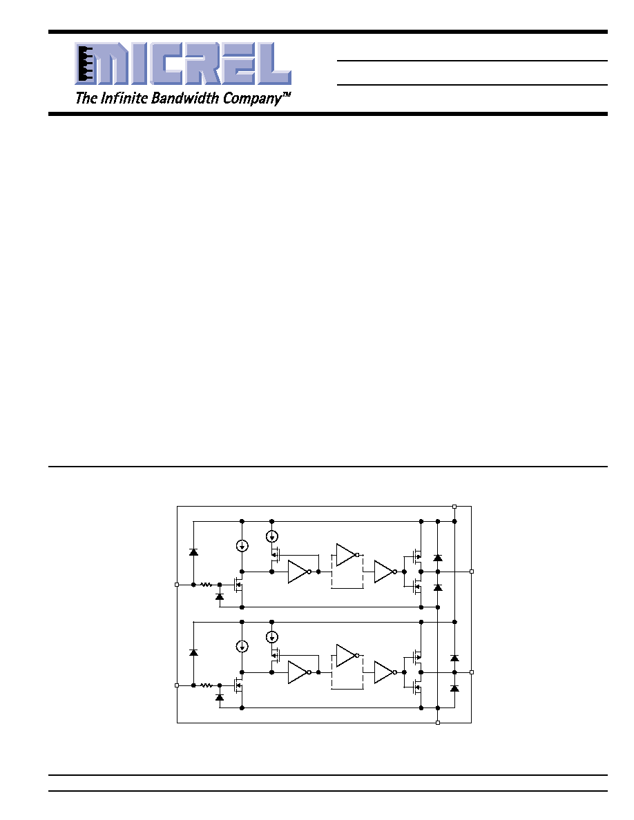
Functional Diagram
INA
OUTA
INVERTING
NONINVERTING
0.1mA
0.6mA
2k
INB
OUTB
INVERTING
NONINVERTING
0.1mA
0.6mA
2k
V
S
GND
Features
∑ Bipolar/CMOS/DMOS construction
∑ Latch-up protection to >500mA reverse current
∑ 1.5A-peak output current
∑ 4.5V to 18V operating range
∑ Low quiescent supply current
4mA at logic 1 input
400
µ
A at logic 0 input
∑ Switches 1000pF in 25ns
∑ Matched rise and rall times
∑ 7
output impedance
∑ < 40ns typical delay
∑ Logic-input threshold independent of supply voltage
∑ Logic-input protection to ≠5V
∑ 6pF typical equivalent input capacitance
∑ 25mV max. output offset from supply or ground
∑ Replaces MIC426/427/428 and MIC1426/1427/1428
∑ Dual inverting, dual noninverting, and inverting/
noninverting configurations
∑ ESD protection
Applications
∑ MOSFET driver
∑ Clock line driver
∑ Coax cable driver
∑ Piezoelectic transducer driver
Micrel, Inc. ∑ 1849 Fortune Drive ∑ San Jose, CA 95131 ∑ USA ∑ tel + 1 (408) 944-0800 ∑ fax + 1 (408) 944-0970 ∑ http://www.micrel.com
MIC4426/4427/4428
Micrel
MIC4426/4427/4428
2
September 1999
Pin Description
Pin Number
Pin Name
Pin Function
1, 8
NC
not internally connected
2
INA
Control Input A: TTL/CMOS compatible logic input.
3
GND
Ground
4
INB
Control Input B: TTL/CMOS compatible logic input.
5
OUTB
Output B: CMOS totem-pole output.
6
V
S
Supply Input: +4.5V to +18V
7
OUTA
Output A: CMOS totem-pole output.
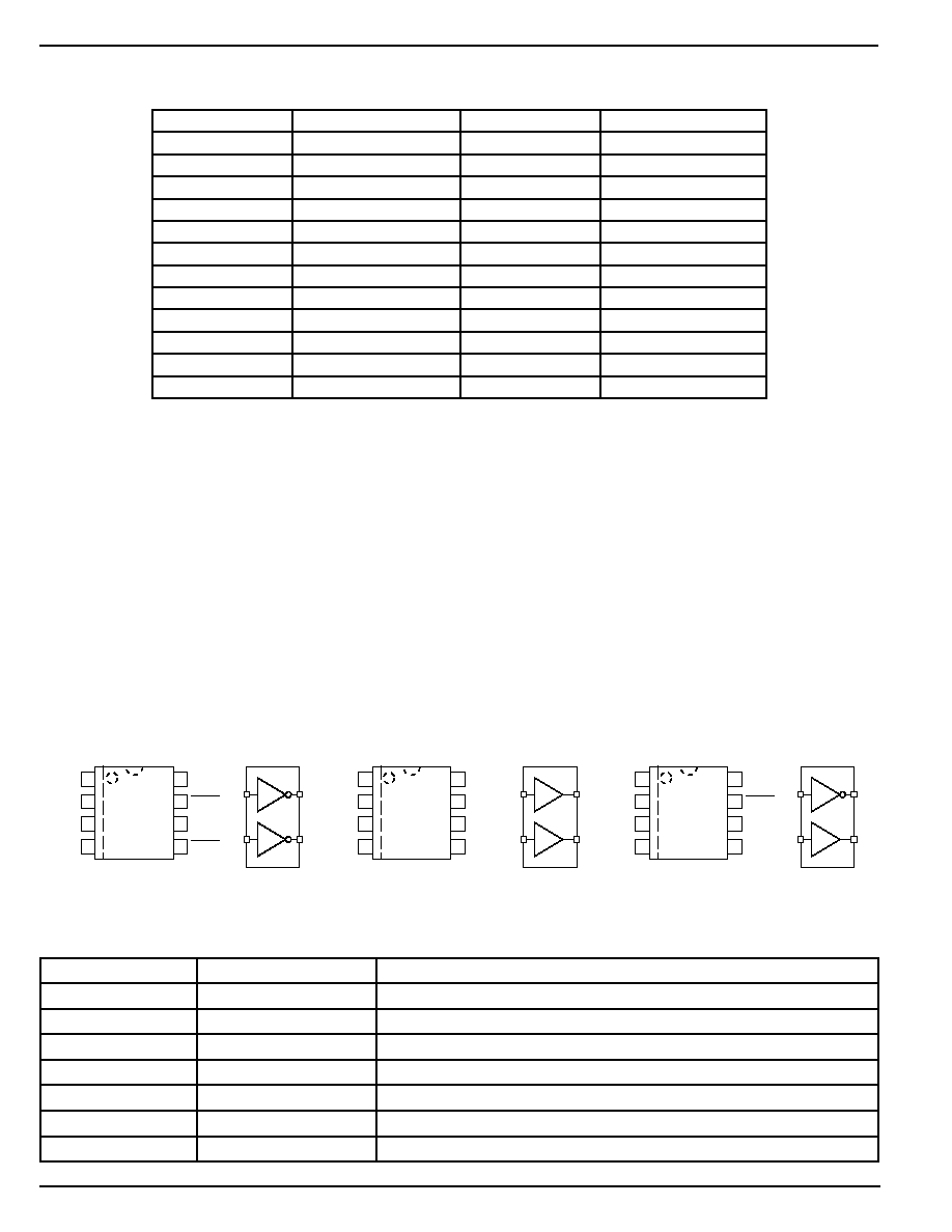
Pin Configuration
1
2
3
4
8
7
6
5
NC
INA
GND
INB
NC
OUTA
V
S
OUTB
MIC4426
Dual
Inverting
A
B
7
5
2
4
MIC4426
MIC4427
MIC4428
A
B
7
5
2
4
A
B
7
5
2
4
1
2
3
4
8
7
6
5
NC
INA
GND
INB
NC
OUTA
V
S
OUTB
MIC4427
Dual
Noninverting
1
2
3
4
8
7
6
5
NC
INA
GND
INB
NC
OUTA
V
S
OUTB
MIC4428
Inverting +
Noninverting
Ordering Information
Part Number
Temperature Range
Package
Configuration
MIC4426AM
≠55
∞
C to +125
∞
C
8-lead SOIC
Dual Inverting
MIC4426BM
≠40
∞
C to +85
∞
C
8-lead SOIC
Dual Inverting
MIC4426BMM
≠40
∞
C to +85
∞
C
8-lead MSOP
Dual Inverting
MIC4426BN
≠40
∞
C to +85
∞
C
8-lead Plastic DIP
Dual Inverting
MIC4427AM
≠55
∞
C to +125
∞
C
8-lead SOIC
Dual Noninverting
MIC4427BM
≠40
∞
C to +85
∞
C
8-lead SOIC
Dual Noninverting
MIC4427BMM
≠40
∞
C to +85
∞
C
8-lead MSOP
Dual Noninverting
MIC4427BN
≠40
∞
C to +85
∞
C
8-pin Plastic DIP
Dual Noninverting
MIC4428AM
≠55
∞
C to +125
∞
C
8-lead SOIC
Inverting + Noninverting
MIC4428BM
≠40
∞
C to +85
∞
C
8-lead SOIC
Inverting + Noninverting
MIC4428BMM
≠40
∞
C to +85
∞
C
8-lead MSOP
Inverting + Noninverting
MIC4428BN
≠40
∞
C to +85
∞
C
8-lead Plastic DIP
Inverting + Noninverting
MIC426/427/428 Device Replacement
Discontinued Number
Replacement
MIC426CM
MIC4426BM
MIC426BM
MIC4426BM
MIC426CN
MIC4426BN
MIC426BN
MIC4426BN
MIC427CM
MIC4427BM
MIC427BM
MIC4427BM
MIC427CN
MIC4427BN
MIC427BN
MIC4427BN
MIC428CM
MIC4428BM
MIC428BM
MIC4428BM
MIC428CN
MIC4428BN
MIC428BN
MIC4428BN
MIC1426/1427/1428 Device Replacement
Discontinued Number
Replacement
MIC1426CM
MIC4426BM
MIC1426BM
MIC4426BM
MIC1426CN
MIC4426BN
MIC1426BN
MIC4426BN
MIC1427CM
MIC4427BM
MIC1427BM
MIC4427BM
MIC1427CN
MIC4427BN
MIC1427BN
MIC4427BN
MIC1428CM
MIC4428BM
MIC1428BM
MIC4428BM
MIC1428CN
MIC4428BN
MIC1428BN
MIC4428BN

September 1999
3
MIC4426/4427/4428
MIC4426/4427/4428
Micrel
Absolute Maximum Ratings
(Note 1)
Supply Voltage (V
S
) .................................................... +22V
Input Voltage (V
IN
) ......................... V
S
+ 0.3V to GND ≠ 5V
Junction Temperature (T
J
) ........................................ 150
∞
C
Storage Temperature ............................... ≠65
∞
C to +150
∞
C
Lead Temperature (10 sec.) ...................................... 300
∞
C
ESD Rating, Note 3
Operating Ratings
(Note 2)
Supply Voltage (V
S
) ..................................... +4.5V to +18V
Temperature Range (T
A
)
(A) ........................................................ ≠55
∞
C to +125
∞
C
(B) .......................................................... ≠40
∞
C to +85
∞
C
Package Thermal Resistance
PDIP
JA
............................................................ 130
∞
C/W
PDIP
JC
............................................................. 42
∞
C/W
SOIC
JA
........................................................... 120
∞
C/W
SOIC
JC
............................................................. 75
∞
C/W
MSOP
JC
......................................................... 250
∞
C/W
Electrical Characteristics
4.5V
V
s
18V; T
A
= 25
∞
C, bold values indicate full specified temperature range; unless noted.
Symbol
Parameter
Condition
Min
Typ
Max
Units
Input
V
IH
Logic 1 Input Voltage
2.4
1.4
V
2.4
1.5
V
V
IL
Logic 0 Input Voltage
1.1
0.8
V
1.0
0.8
V
I
IN
Input Current
0
V
IN
V
S
≠1
1
µ
A
Output
V
OH
High Output Voltage
V
S
≠0.025
V
V
OL
Low Output Voltage
0.025
V
R
O
Output Resistance
I
OUT
= 10mA, V
S
= 18V
6
10
8
12
I
PK
Peak Output Current
1.5
A
I
Latch-Up Protection
withstand reverse current
>500
mA
Switching Time
t
R
Rise Time
test Figure 1
18
30
ns
20
40
ns
t
F
Fall Time
test Figure 1
15
20
ns
29
40
ns
t
D1
Delay Tlme
test Flgure 1
17
30
ns
19
40
ns
t
D2
Delay Time
test Figure 1
23
50
ns
27
60
ns
t
PW
Pulse Width
test Figure 1
400
ns
Power Supply
I
S
Power Supply Current
V
INA
= V
INB
= 3.0V
1.4
4.5
mA
1.5
8
mA
I
S
Power Supply Current
V
INA
= V
INB
= 0.0V
0.18
0.4
mA
0.19
0.6
mA
Note 1.
Exceeding the absolute maximum rating may damage the device.
Note 2.
The device is not guaranteed to function outside its operating rating.
Note 3.
Devices are ESD sensitive. Handling precautions recommended.

MIC4426/4427/4428
Micrel
MIC4426/4427/4428
4
September 1999
Test Circuits
A
B
INA
INB
2
4
MIC4427
5
7
OUTA
1000pF
6
V
S
= 18V
0.1µF
4.7µF
OUTB
1000pF
Figure 2a. Noninverting Configuration
90%
10%
t
R
10%
0V
5V
t
F
V
S
OUTPUT
INPUT
90%
0V
t
D1
t
D2
t
PW
2.5V
Figure 2b. Noninverting Timing
A
B
INA
INB
2
4
MIC4426
5
7
OUTA
1000pF
6
V
S
= 18V
0.1µF
4.7µF
OUTB
1000pF
Figure 1a. Inverting Configuration
t
D1
90%
10%
t
F
10%
0V
5V
t
D2
t
R
V
S
OUTPUT
INPUT
90%
0V
2.5V
t
PW
Figure 1b. Inverting Timing
September 1999
5
MIC4426/4427/4428
MIC4426/4427/4428
Micrel
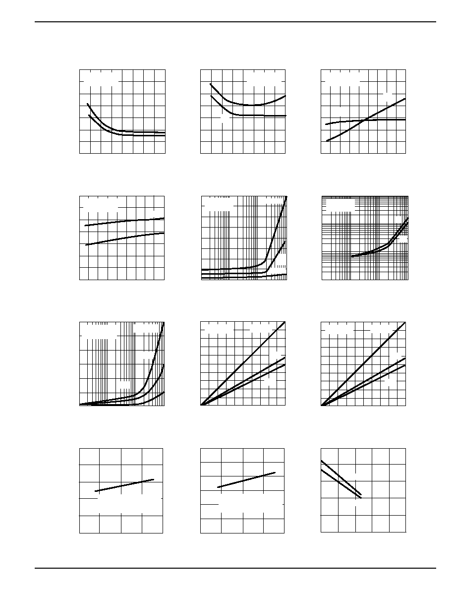
Electrical Characteristics
Rise and Fall Time vs.
Supply Voltage
0
5
20
10
15
t
F
SUPPLY VOLTAGE (V)
70
60
50
40
10
0
TIME
(ns)
20
30
Delay Time vs. Supply Voltage
0
5
20
10
15
SUPPLY VOLTAGE (V)
35
30
25
20
5
0
TIME
(ns)
10
15
40
30
10
TIME
(ns)
20
-25 0
150
25 50
TEMPERATURE (
∞
C)
75 100 125
Delay Time vs. Temperature
35
30
25
20
5
0
TIME
(ns)
10
15
-25
0
150
25 50
TEMPERATURE (
∞
C)
75 100 125
t
D1
Supply Current vs.
Capacitive Load
80
70
60
50
20
0
SUPPLY CURRENT (mA)
30
40
10
400kHz
200
kHz
20kHz
10
10000
100
CAPACITIVE LOAD (pF)
1000
1k
100
10
1
TIME
(ns)
10
10000
100
CAPACITIVE LOAD (pF)
1000
Rise and Fall Time vs.
Capacitive Load
t
R
t
F
Supply Current vs. Frequency
V = 18V
S
10 V
5 V
20
0
SUPPLY CURRENT (mA)
30
10
1
1000
10
FREQUENCY (kHz)
100
High Output vs. Current
| V ≠ V | (V)
S
OUT
CURRENT SOURCED (mA)
Low Output vs. Current
1.20
0.96
0
0.48
0.72
0.24
0 10
CURRENT SUNK (mA)
20 30 40 50 60 70 80 90 100
10 V
15 V
OUTPUT VOLTAGE (V)
Rise and Fall Time
vs. Temperature
1.20
0.96
0
0.48
0.72
0.24
0 10 20 30 40 50 60 70 80 90 100
10 V
15 V
-50
t
R
-50
-75
t
R
t
F
-75
t
D2
t
D1
t
D2
C = 1000pF
T = 25
∞
C
L
A
C = 1000pF
T = 25
∞
C
L
A
C = 1000pF
V = 18V
L
S
C = 1000pF
V = 18V
L
S
T = 25
∞
C
V = 18V
A
S
T = 25
∞
C
V = 18V
A
S
T = 25
∞
C
C = 1000pF
L
A
T = 25
∞
C
A
V = 5V
C
T = 25
∞
C
A
V = 5V
S
Quiescent Power Supply
Current vs. Supply Voltage
Package Power Dissipation
25
50
150
75
100
AMBIENT TEMPERATURE (
∞
C)
1000
750
250
0
500
Quiescent Power Supply
Current vs. Supply Voltage
0
0.5
2.5
1.0
1.5
SUPPLY CURRENT (mA)
20
15
5
0
SUPPLY VOLTAGE (V)
10
2.0
125
SUPPLY CURRENT (
µ
A)
15
10
0
5
0
50
100
150
200
300
400
20
SUPPLY VOLTAGE (V)
MAXIMUM PACKAGE
POWER DISSIPATION (mW)
1250
NO LOAD
BOTH INPUTS LOGIC "1"
T = 25
∞
C
A
NO LOAD
BOTH INPUTS LOGIC "0"
T = 25
∞
C
A
SOIC
PDIP