 | –≠–ª–µ–∫—Ç—Ä–æ–Ω–Ω—ã–π –∫–æ–º–ø–æ–Ω–µ–Ω—Ç: KS8995XA | –°–∫–∞—á–∞—Ç—å:  PDF PDF  ZIP ZIP |
May 2005
1
M9999-051305
KS8995XA
Micrel, Inc.
KS8995XA
Integrated 5-Port 10/100 QoS Switch
Rev. 2.3
General Description
The KS8995XA is a highly integrated Layer-2 quality of
service (QoS) switch with optimized bill of materials (BOM)
cost for low port count, cost-sensitive 10/100Mbps switch
systems. It also provides an extensive feature set including
three different QoS priority schemes, a dual MII interface for
BOM cost reduction, rate limiting to offload CPU tasks,
software and hardware power-down, a MDC/MDIO control
interface and port mirroring/monitoring to effectively address
both current and emerging Fast Ethernet applications.
The KS8995XA contains five 10/100 transceivers with pat-
ented mixed-signal low-power technology, five media access
control (MAC) units, a high-speed non-blocking switch fabric,
a dedicated address lookup engine, and an on-chip frame
buffer memory.
All PHY units support 10BASE-T and 100BASE-TX. In addi-
tion, two of the PHY units support 100BaseFX (Ports 4 and 5).
Features
∑ Integrated switch with five MACs and five Fast Ethernet
transceivers fully compliant to IEEE 802.3u standard
∑ Shared memory based switch fabric with fully non-
blocking configuration
∑ 10BASE-T, 100BASE-TX and 100BASE-FX modes
(FX in Ports 4 and 5)
∑ Dual MII configuration: MII-Switch (MAC or PHY
mode MII) and MII-P5 (PHY mode MII)
∑ VLAN ID tag/untag options, per-port basis
∑ Enable/disable option for huge frame size up to
1916 bytes per frame
∑ Broadcast storm protection with percent control ≠
global and per-port basis
∑ Optimization for fiber-to-copper media conversion
∑ Full-chip hardware power-down support (register
configuration not saved)
∑ Per-port-based software power-save on PHY
(idle link detection, register configuration preserved)
∑ QoS/CoS packets prioritization supports: per port,
802.1p and DiffServ-based
Micrel, Inc. ∑ 2180 Fortune Drive ∑ San Jose, CA 95131 ∑ USA ∑ tel + 1 (408) 944-0800 ∑ fax + 1 (408) 474-1000 ∑ http://www.micrel.com
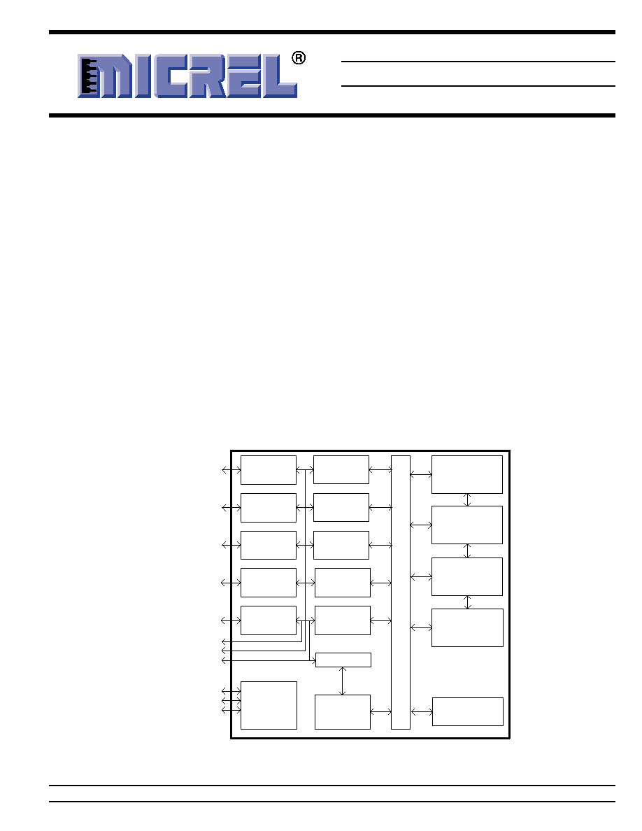
Functional Diagram
1K Look-Up
Engine
Queue
Mgmnt
10/100
MAC 1
Buffer
Mgmnt
Frame
Buffers
FIFO
, Flo
w Contro
l, VLAN
T
agging, P
r
ior
ity
10/100
MAC 2
10/100
MAC 3
10/100
MAC 4
10/100
MAC 5
SNI
10/100
T/Tx 1
10/100
T/Tx 2
10/100
T/Tx 3
10/100
T/Tx/Fx 4
10/100
T/Tx/Fx 5
EEPROM
I/F
LED I/F
Auto
MDI/MDI-X
MII-SW or SNI
LED0[5:1]
LED1[5:1]
LED2[5:1]
Control
Registers
MII-P5
MDC, MDI/O
KS8995XA
Auto
MDI/MDI-X
Auto
MDI/MDI-X
Auto
MDI/MDI-X
Auto
MDI/MDI-X

KS8995XA
Micrel, Inc.
M9999-051305
2
May 2005
Features
(continued)
∑ 802.1p/q tag insertion or removal on a per-port basis
(egress)
∑ Port-based VLAN support
∑ MDC and MDI/O interface support to access the MII
PHY control registers (not all control registers)
∑ MII local loopback support
∑ On-chip 64Kbyte memory for frame buffering (not
shared with 1K unicast address table)
∑ 1.4Gbps high performance memory bandwidth
∑ Wire-speed reception and transmission
∑ Integrated look-up engine with dedicated 1K unicast
MAC addresses
∑ Automatic address learning, address aging and address
migration
∑ Full-duplex IEEE 802.3x and half-duplex back pressure
flow control
∑ Comprehensive LED support
∑ 7-wire SNI support for legacy MAC interface
∑ Automatic MDI/MDI-X crossover for plug-and-play
∑ Disable automatic MDI/MDI-X option
∑ Low power
Core: 1.8V
I/O: 2.5 or 3.3V
∑ 0.18µm CMOS technology
∑ Commercial temperature range: 0∞C to +70∞C
∑ Available in 128-pin PQFP package
Applications
∑ Broadband gateway/firewall/VPN
∑ Integrated DSL or cable modem multi-port router
∑ Wireless LAN access point plus gateway
∑ Home networking expansion
∑ Standalone 10/100 switch
∑ Hotel/campus/MxU gateway
∑ Enterprise VoIP gateway/phone
∑ FTTx customer premise equipment
∑ Media converter
Ordering Information
Part Number
Temp. Range
Package
Lead Finish
KS8995XA
0∞C to +70∞C
128-Pin PQFP
Standard
KSZ8995XA
0∞C to +70∞C
128-Pin PQFP
Pb-Free

May 2005
3
M9999-051305
KS8995XA
Micrel, Inc.
Revision History
Revision
Date
Summary of Changes
2.0
10/15/03
Created.
2.1
4/1/04
Editorial changes on TTL input and output electrical characteristics.
2.2
1/19/05
Insert recommeneded reset circuit.
2.3
4/13/05
Switched pins names for pins 7 & 8 on page 16.
Changed VDDIO to 3.3V.
Changed Jitter to 16 ns Max.

KS8995XA
Micrel, Inc.
M9999-051305
4
May 2005
Table of Contents
System Level Applications .............................................................................................................................................................. 6
Pin Description (by Number) ........................................................................................................................................................... 8
Pin Description (by Name) ............................................................................................................................................................ 13
Pin Configuration ........................................................................................................................................................................... 18
Introduction
............................................................................................................................................................................ 19
Functional Overview: Physical Layer Transceiver ..................................................................................................................... 19
100BASE-TX Transmit ............................................................................................................................................................ 19
100BASE-TX Receive ............................................................................................................................................................. 19
PLL Clock Synthesizer ............................................................................................................................................................ 19
Scrambler/De-scrambler (100BASE-TX only) ......................................................................................................................... 19
100BaseFX Operation ............................................................................................................................................................. 19
100BaseFX Signal Detection ................................................................................................................................................... 20
100BaseFX Far End Fault ....................................................................................................................................................... 20
10BASE-T Transmit ................................................................................................................................................................. 20
10BASE-T Receive .................................................................................................................................................................. 20
Power Management ................................................................................................................................................................ 20
MDI/MDI-X Auto Crossover ..................................................................................................................................................... 20
Auto-Negotiation ...................................................................................................................................................................... 20
Functional Overview: Switch Core ............................................................................................................................................... 21
Address Look Up ..................................................................................................................................................................... 21
Learning
............................................................................................................................................................................ 21
Migration
............................................................................................................................................................................ 21
Aging
............................................................................................................................................................................ 21
Switching Engine ..................................................................................................................................................................... 21
MAC (Media Access Controller) Operation ............................................................................................................................. 22
Inter-Packet Gap ............................................................................................................................................................. 22
Backoff Algorithm ............................................................................................................................................................ 22
Late Collision .................................................................................................................................................................. 22
Illegal Frame ................................................................................................................................................................... 22
Flow Control .................................................................................................................................................................... 22
Half-Duplex Back Pressure ............................................................................................................................................. 22
Broadcast Storm Protection ............................................................................................................................................ 23
MII Interface Operation .................................................................................................................................................................. 23
SNI Interface Operation ................................................................................................................................................................. 25
Advanced Functionality ................................................................................................................................................................. 25
QoS Support ............................................................................................................................................................................ 25
Rate Limit Support ................................................................................................................................................................... 27
Configuration Interface ............................................................................................................................................................ 28
I
2
C Master Serial Bus Configuration ............................................................................................................................... 28
MII Management Interface (MIIM) .................................................................................................................................................. 28
Register Map
............................................................................................................................................................................ 29
Global Registers ...................................................................................................................................................................... 29
Register 0 (0x00): Chip ID0 ............................................................................................................................................ 29
Register 1 (0x01): Chip ID1/Start Switch ....................................................................................................................... 29
Register 2 (0x02): Global Control 0 ................................................................................................................................ 29
Register 3 (0x03): Global Control 1 ................................................................................................................................ 30
Register 4 (0x04): Global Control 2 ................................................................................................................................ 31
Register 5 (0x05): Global Control 3 ................................................................................................................................ 31
Register 6 (0x06): Global Control 4 ................................................................................................................................ 32
Register 7 (0x07): Global Control 5 ................................................................................................................................ 32

May 2005
5
M9999-051305
KS8995XA
Micrel, Inc.
Register 8 (0x08): Global Control 6 ................................................................................................................................ 32
Register 9 (0x09): Global Control 7 ................................................................................................................................ 32
Register 10 (0x0A): Global Control 8 ............................................................................................................................. 32
Register 11 (0x0B): Global Control 9 ............................................................................................................................. 33
Port Registers .......................................................................................................................................................................... 33
Register 16 (0x10): Port 1 Control 0 .............................................................................................................................. 33
Register 17 (0x11): Port 1 Control 1 .............................................................................................................................. 34
Register 18 (0x12): Port 1 Control 2 .............................................................................................................................. 34
Register 19 (0x13): Port 1 Control 3 .............................................................................................................................. 35
Register 20 (0x14): Port 1 Control 4 .............................................................................................................................. 35
Register 21 (0x15): Port 1 Control 5 .............................................................................................................................. 35
Register 22 (0x16): Port 1 Control 6 .............................................................................................................................. 35
Register 23 (0x17): Port 1 Control 7 .............................................................................................................................. 36
Register 24 (0x18): Port 1 Control 8 .............................................................................................................................. 36
Register 25 (0x19): Port 1 Control 9 .............................................................................................................................. 36
Register 26 (0x1A): Port 1 Control 10 ............................................................................................................................ 36
Register 27 (0x1B): Port 1 Control 11 ............................................................................................................................ 37
Register 28 (0x1C): Port 1 Control 12 ............................................................................................................................ 37
Register 29 (0x1D): Port 1 Control 13 ............................................................................................................................ 38
Register 30 (0x1E): Port 1 Status 0 ............................................................................................................................... 39
Register 31 (0x1F): Port 1 Control 14 ............................................................................................................................ 39
Advanced Control Registers .................................................................................................................................................... 39
Register 96 (0x60): TOS Priority Control Register 0 ...................................................................................................... 39
Register 97 (0x61): TOS Priority Control Register 1 ...................................................................................................... 40
Register 98 (0x62): TOS Priority Control Register 2 ...................................................................................................... 40
Register 99 (0x63): TOS Priority Control Register 3 ...................................................................................................... 40
Register 100 (0x64): TOS Priority Control Register 4 .................................................................................................... 40
Register 101 (0x65): TOS Priority Control Register 5 .................................................................................................... 40
Register 102 (0x66): TOS Priority Control Register 6 .................................................................................................... 40
Register 103 (0x67): TOS Priority Control Register 7 .................................................................................................... 40
Register 104 (0x68): MAC Address Register 0 .............................................................................................................. 40
Register 105 (0x69): MAC Address Register 1 .............................................................................................................. 40
Register 106 (0x6A): MAC Address Register 2 .............................................................................................................. 40
Register 107 (0x6B): MAC Address Register 3 .............................................................................................................. 40
Register 108 (0x6C): MAC Address Register 4 ............................................................................................................. 40
Register 109 (0X6D): MAC Address Register 5 ............................................................................................................. 40
MIIM Registers ........................................................................................................................................................................ 40
Register 0: MII Control ................................................................................................................................................... 40
Register 1: MII Status .................................................................................................................................................... 41
Register 2: PHYID HIGH ................................................................................................................................................ 41
Register 3: PHYID LOW ................................................................................................................................................ 41
Register 4: Advertisement Ability ................................................................................................................................... 41
Register 5: Link Partner Ability ....................................................................................................................................... 42
Absolute Maximum Ratings .......................................................................................................................................................... 43
Operating Ratings .......................................................................................................................................................................... 43
Electrical Characteristics .............................................................................................................................................................. 43
Timing Diagrams ............................................................................................................................................................................ 45
Selection of Isolation Transformers ............................................................................................................................................. 50
Package Information ...................................................................................................................................................................... 51