December 2003
1
M9999-122303
LM2574
Micrel
LM2574
52kHz Simple 0.5A Buck Regulator
General Description
The LM2574 family is a series of easy to use fixed and
adjustable switching voltage regulators. The LM2574 con-
tains all of the active circuitry necessary to construct a
stepdown (buck) switching regulator and requires a minimum
of external components.
The LM2574 is available in 3.3V and 5V fixed output versions,
or an adjustable version with an output voltage range of 1.23V
to 37V. Output voltage is guaranteed to
±
4% for specified
input and load conditions.
The LM2574 can supply 0.5A while maintaining excellent line
and load regulation. The output switch includes cycle-by-
cycle current limiting, as well as thermal shutdown for full
protection under fault conditions.
An external shutdown connection selects operating or standby
modes. Standby current is less than 200
µ
A.
Heat sinks are generally unnecessary due the regulator's
high efficiency. Adequate heat transfer is usually provided by
soldering all package pins to a printed circuit board.
The LM2574 includes internal frequency compensation and
an internal 52kHz fixed frequency oscillator guaranteed to
±
10% of the frequency.
Circuits constructed around the LM2574 use a standard
series of inductors which are available from several different
manufacturers.
All support documentation can be found on Micrel's web
site at www.micrel.com.
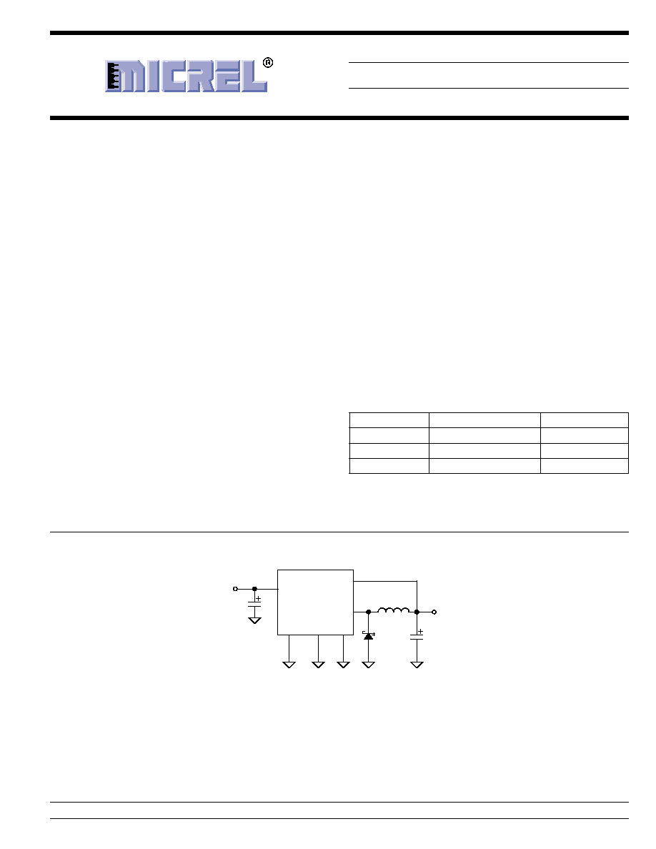
Typical Application
V
IN
PWR
GND
SIG
GND
ON/
OFF
OUT
FB
LM2574
C
IN
22µF
40V MAX
UNREGULATED
DC IN
REGULATED
OUTPUT
0.5A
11DQ05
C
OUT
220µF
330µH
Figure 1. Fixed Output Regulator Circuit
Features
∑ 3.3V, 5V, 12V, and adjustable output versions
∑ Adjustable version output 1.23V to 37V
±
4% max. over
line and load conditions.
∑ Guaranteed 0.5A output current
∑ Wide input voltage, up to 40V
∑ Thermal shutdown and current limit protection
∑ Requires only 4 external components.
∑ Shutdown capability (standby mode)
∑ Low power standby mode < 200
µ
A Typical
∑ High-efficiency
∑ 52kHz fixed frequency internal oscillator
∑ Uses standard inductors
Applications
∑ Simple high-efficiency step-down (buck) regulator
∑ Efficient pre-regulator for linear regulators
∑ On-card switching regulators
∑ Positive to negative converter (buck-boost)
Ordering Information
Part Number
Junction Temp. Range
Package
LM2574BN
≠40
∞
C to +85
∞
C
8-pin Plastic DIP
LM2574-3.3BN
≠40
∞
C to +85
∞
C
8-pin Plastic DIP
LM2574-5.0BN
≠40
∞
C to +85
∞
C
8-pin Plastic DIP
Micrel, Inc. ∑ 1849 Fortune Drive ∑ San Jose, CA 95131 ∑ USA ∑ tel + 1 (408) 944-0800 ∑ fax + 1 (408) 944-0970 ∑ http://www.micrel.com
LM2574
Micrel
M9999-122303
2
December 2003
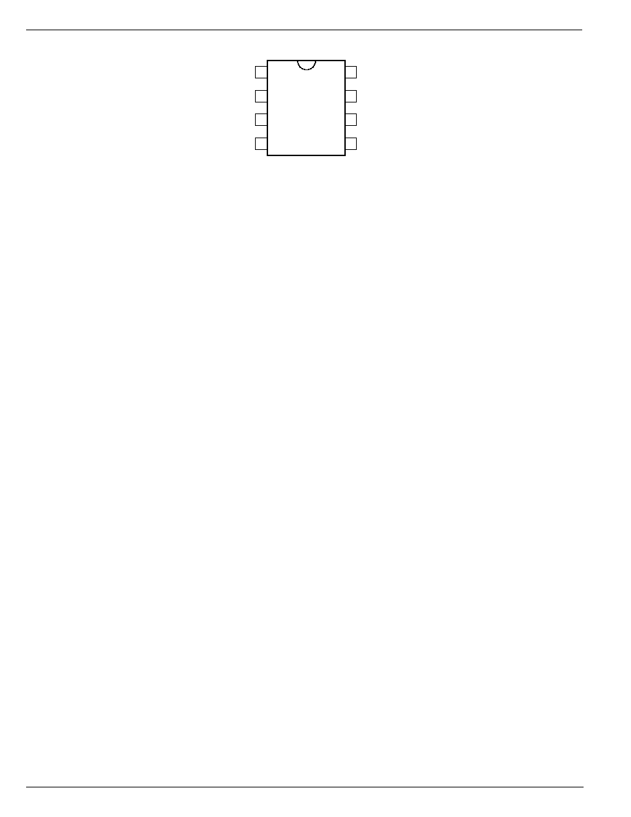
Pin Configuration
FB 1
SIG GND 2
ON/OFF 3
PWR GND 4
8 NC
7 OUTPUT
6 NC
5 VIN
8-Pin DIP (N)

December 2003
3
M9999-122303
LM2574
Micrel
Absolute Maximum Ratings
(1)
Maximum Supply Voltage
LM2574 ..................................................................... 45V
OFF Pin Input Voltage ................................ ≠0.3V
V
V
IN
Output Voltage to Ground (Steady State) ..................... ≠1V
Power Dissipation .................................... Internally Limited
Storage Temperature Range (T
S
) ............ ≠65
∞
C to +150
∞
C
Minimum ESD Rating
C = 100pF, R = 1.5k
............................................... 2kV
FB Pin ....................................................................... 1kV
Lead Temperature (soldering, 10 sec.) ..................... 260
∞
C
Operating Ratings
(1)
Supply Voltage
LM2574 ..................................................................... 40V
Temperature Range
LM2574 ......................................... ≠40
∞
C
T
J
+125
∞
C
Maximum Junction Temperature (T
J ...............................
150
∞
C
Electrical Characteristics
(2)
Specifications with standard typeface are for T
J
= 25
∞
C, and those with boldface type apply over full Operating Temperature Range.
Unless otherwise specified, V
IN
= 12V, and I
LOAD
= 100mA.
Symbol
Parameter
Condition
Min
Typ
Max
Units
System Parameters, Adjustable Regulators
(3)
, Test Circuit
Figure 2
V
OUT
Feedback Voltage
V
IN
= 12V, I
LOAD
= 0.1A, V
OUT
= 5V
1.217
1.230
1.243
V
V
OUT
Feedback Voltage
0.1A
I
LOAD
0.5A, 7V
V
IN
40V,
1.193
1.230
1.267
V
(LM2574)
V
OUT
= 5V
1.180
1.280
V
Efficiency
V
IN
= 12V, I
LOAD
= 0.1A, V
OUT
= 5V
78
%
System Parameters, 3.3V Regulators
(3)
, Test Circuit
Figure 3
V
OUT
Output Voltage
V
IN
= 12V, I
LOAD
= 0.1A, V
OUT
= 3.3V
3.234
3.3
3.366
V
V
OUT
Output Voltage
0.1A
I
LOAD
0.5A, 4.75V
V
IN
40V,
3.168
3.3
3.432
V
(LM2574-3.3)
V
OUT
= 3.3V
3.135
3.465
V
Efficiency
V
IN
= 12V, I
LOAD
= 0.1A
73
%
System Parameters, 5V Regulators
(3)
, Test Circuit
Figure 3
V
OUT
Output Voltage
V
IN
= 12V, I
LOAD
= 0.1A, V
OUT
= 5V
4.900
5.0
5.100
V
V
OUT
Output Voltage
0.1A
I
LOAD
0.5A, 7V
V
IN
40V,
4.800
5.0
5.200
V
(LM2574-5.0)
V
OUT
= 5V
4.750
5.250
V
Efficiency
V
IN
= 12V, I
LOAD
= 0.1A, V
OUT
= 5V
78
%
Notes:
1.
"Absolute Maximum Ratings"
indicate limits beyond which damage to the device may occur.
"Operating Ratings"
indicate for which the device is
intended to be functional, but do not guarantee specific performance limits. For guaranteed specifications and test conditions, see
"Electrical
Characteristics."
2. All limits guaranteed at room temperature (standard type face) and at temperature extremes (bold type face). All room temperature limits are 100%
production tested. All limits at temperature extremes are guaranteed via testing.
3. External components such as the catch diode, inductor, input and output capacitors can affect switching regulator system performance.
When the LM2574 is used as shown in Figure 1 test circuit, system performance will be shown in system parameters section of
"Electrical Charac-
teristics."

LM2574
Micrel
M9999-122303
4
December 2003
Electrical Characteristics
Symbol
Parameter
Condition
Min
Typ
Max
Units
Device Parameters, Adjustable Regulator
I
B
Feedback Bias Current
V
OUT
= 5V
50
100
nA
500
nA
Device Parameters, Fixed and Adjustable Regulators
f
o
Oscillator Frequency
Note 8
47
52
58
kHz
42
63
kHz
V
SAT
Saturation Voltage
I
OUT
= 0.5A
(4)
0.8
1.2
V
1.4
V
DC
Max Duty Cycle (ON)
Note 5
93
98
%
I
CL
Current Limit
Peak Current, t
ON
3
µ
s
(4)
0.7
1.0
1.6
A
0.65
1.8
I
L
Output Leakage Current
V
IN
, Note 6, Output = 0V
2
mA
Note 6, Output = ≠1V
7.5
30
I
Q
Quiescent Current
Note 6
5
10
mA
I
STBY
Standby Quiescent Current
ON/OFF Pin = 5V (OFF)
50
200
µ
A
JA
Thermal Resistance
N Package, Junction to Ambient
(7)
85
∞
C/W
On/Off Control, Fixed and Adjustable Regulators Test Circuit
Figures 2, 3
V
IH
ON/OFF Input Level
V
OUT
= 0V
2.2
1.4
V
2.4
V
V
IL
ON/OFF Input Level
V
OUT
= 5V
1.2
1.0
V
0.8
V
I
IH
ON/OFF Logic Current
ON/OFF = 5V (OFF)
4
30
µ
A
I
IL
ON/OFF Logic Current
ON/OFF = 0V (ON)
0.01
10
µ
A
Notes:
4. Output (pin 2) sourcing current. No diode, inductor, or capacitor connected to input.
5. Feedback (pin 4) removed from output and connected to 0V.
6. Feedback (pin 4) removed from output and connected to 12V to force the output transistor OFF.
7. Junction-to-ambient thermal resistance with approximately 1 square inches of PC board copper surrounding the leads.
Test Circuit
V
IN
PWR
GND
SIG
GND
ON/
OFF
OUT
FB
LM2574
(adjustable)
C
IN
22µF
11DQ06
C
OUT
220µF
330µH
3.09k
1k
Load
Figure 2. Adjustable Regulator Test Circuit
V
IN
PWR
GND
SIG
GND
ON/
OFF
OUT
FB
LM2574≠
3.3, 5
C
IN
22
µ
F
11DQ06
C
OUT
220
µ
F
330
µ
H
Load
Figure 3. Fixed Regulator Test Circuit
December 2003
5
M9999-122303
LM2574
Micrel
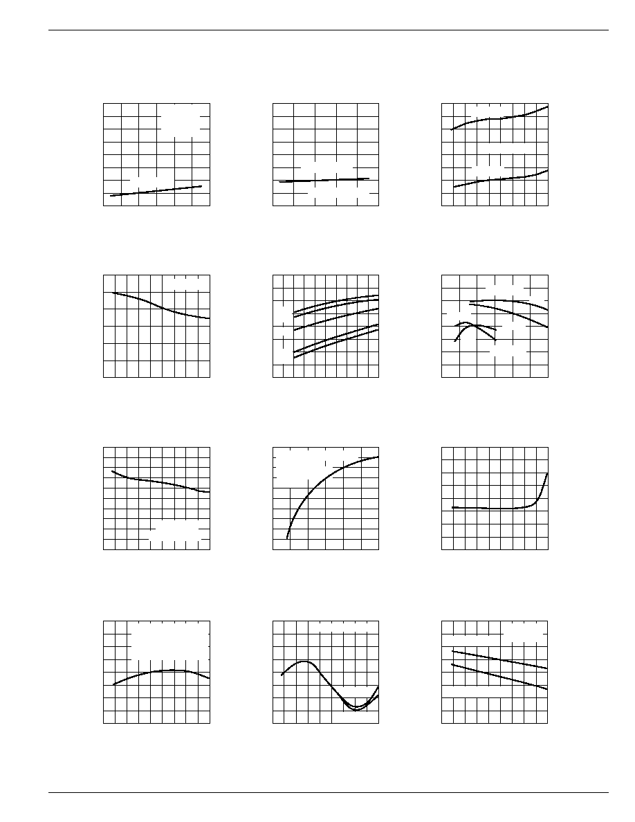
Typical Characteristics
(Circuit of Figure 1)
Supply Current
INPUT VOLTAGE (V)
SUPPLY CURRENT (mA)
20
Measured at
Ground Pin
TJ = 25∞C
VOUT = 5V
18
16
14
12
10
8
6
4
0
10
20
30
40
50
60
ILOAD to 0.5A
Supply Current
vs. Duty Cycle
DUTY CYCLE (%)
20.0
17.5
15.0
12.5
10.0
7.5
5.0
2.5
0
0
20
40
60
80
100
VIN from 7V to 40V
ILOAD = 100 mA
SUPPLY CURRENT (mA)
JUNCTION TEMPERATURE (∞C)
200
150
100
50
0
-75
VIN = 12V
STANDBY QUIESCENT CURRENT (µA)
Standby
Quiescent Current
VIN = 40V
-50 -25
0 25 50 75 100 125 150
Current Limit
JUNCTION TEMPERATURE (∞C)
1.5
1
0.5
0
-75
VIN = 25V
OUTPUT CURRENT (A)
INPUT VOLTAGE (V)
100
EFFICIENCY (%)
Efficiency
VOUT = 12V
-50 -25
0 25 50 75 100 125 150
95
90
85
80
75
70
65
60
100 mA
100 mA
VOUT = 3V
0.5A
0.5A
0
5
10 15 20 25 30
35 40
Minimum Operating
Voltage
JUNCTION TEMPERATURE (∞C)
5.0
ILOAD = 100 mA
INPUT VOLTAGE (V)
Line Regulation
INPUT VOLTAGE (V)
14
0
NORMALIZED FEEDBACK VOLTAGE (mV)
JUNCTION TEMPERATURE (∞C)
100
-100
-75
STANDBY QUIESCENT CURRENT (nA)
Feedback Pin Current
-50 -25 0
25 50 75 100 125 150
VOUT = 1.23V
4.5
4.0
3.5
3.0
2.5
2.0
1.5
1.0
0.5
0
-75 -50 -25 0
25 50 75 100 125 150
12
10
8
6
4
2
0
-2
-4
-6
5
10
15
20
25
30
75
50
25
0
-25
-50
-75
JUNCTION TEMPERATURE (∞C)
+8
-8
-75
NORMALIZED FREQUENCY (%)
Oscillator Frequency
-50 -25
0 25 50 75 100 125 150
+6
+4
+2
0
-2
-4
--6
VIN = 12V
VIN = 40V
Normalized at 25∞C
Normalized to VIN = 10V
VOUT = 5V
ILOAD = 100mA
TJ = 25
VON/OFF = 5V
Switch
Saturation Voltage
SWITCH CURRENT (A)
1.1
-55∞C
0.9
0.7
0.5
0.3
0
SATURATION VOLTAGE (V)
0.1
0.2
0.3
0.4
0.5
25∞C
125∞C
150∞C
-40∞C
Dropout Voltage
JUNCTION TEMPERATURE (∞C)
INPUT-OUTPUT DIFFERENTIAL (V)
2.0
-75 -50 -25
0 25 50 75 100 125 150
VOUT = 5%
RIND = 0.2
ILOAD = 0.5A
ILOAD = 100 mA
1.5
1.0
0.5
0
Normalized
Output Voltage
JUNCTION TEMPERATURE (∞C)
OUTPUT VOLTAGE CHANGE (mV)
100
75
50
25
0
-25
-50
-75
-100
-75 -50 -25
0
25 50 75 100 125 150
VIN = 12V
ILOAD = 100mA
Normalized to TJ = 25∞C
VOUT = 5V