August 1999
1
M2575
LM2575
Micrel
LM2575
52kHz Simple 1A Buck Regulator
General Description
The LM2575 series of monolithic integrated circuits provide
all the active functions for a step-down (buck) switching
regulator. Fixed versions are available with a 3.3V, 5V, 12V,
fixed output. Adjustable versions have an output voltage
range from 1.23V to 37V. Both versions are capable of driving
a 1A load with excellent line and load regulation.
These regulators are simple to use because they require a
minimum number of external components and include internal
frequency compensation and a fixed-frequency oscillator.
The LM2575 series offers a high efficiency replacement for
popular three-terminal adjustable linear regulators. It
substantially reduces the size of the heat sink, and in many
cases no heat sink is required.
A standard series of inductors available from several different
manufacturers are ideal for use with the LM2575 series. This
feature greatly simplifies the design of switch-mode power
supplies.
The feedback voltage is guaranteed to
±
2% tolerance for
adjustable versions, and the output voltage is guaranteed to
±
3% for fixed versions, within specified input voltages and
output load conditions. The oscillator frequency is guaranteed
to
±
10%. External shutdown is included, featuring less than
200
µ
A standby current. The output switch includes cycle-by-
cycle current limiting and thermal shutdown for full protection
under fault conditions.
870 20
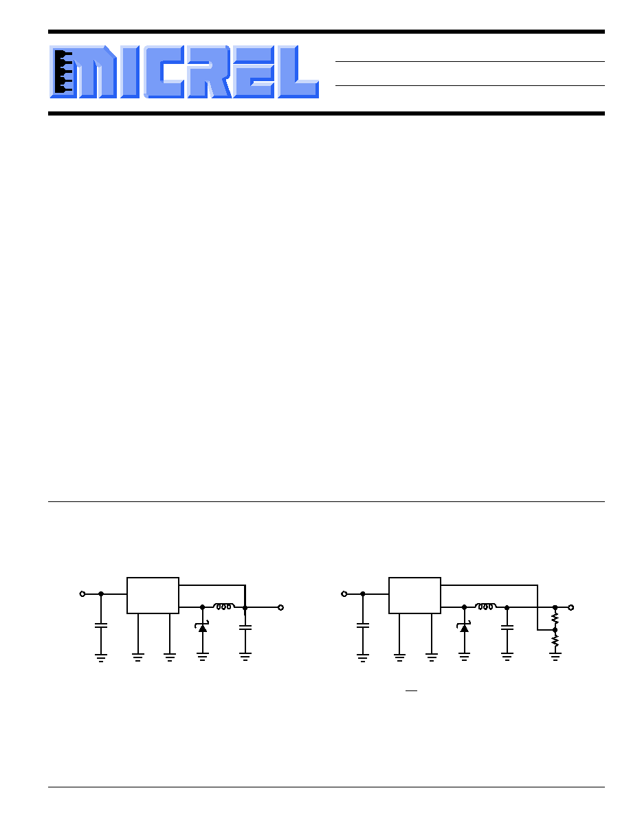
Typical Applications
Features
∑ 3.3V, 5V, 12V, and adjustable output versions
∑ Voltage over specified line and load conditions:
Fixed version:
±
3% max. output voltage
Adjustable version:
±
2% max. feedback voltage
∑ Guaranteed 1A output current
∑ Wide input voltage range:
4V to 40V
∑ Wide output voltage range
1.23V to 37V
∑ Requires only 4 external components
∑ 52kHz fixed frequency internal oscillator
∑ Low power standby mode I
Q
typically < 200
µ
A
∑ 80% efficiency (adjustable version typically > 80%)
∑ Uses readily available standard inductors
∑ Thermal shutdown and current limit protection
∑ 100% electrical thermal limit burn-in
Applications
∑ Simple high-efficiency step-down (buck) regulator
∑ Efficient pre-regulator for linear regulators
∑ On-card switching regulators
∑ Positive to negative converter (inverting Buck-Boost)
∑ Isolated Flyback Converter using minimum number of
external components
∑ Negative Boost Converter
R2
R1
7V≠40V
Unregulated
DC Input
LM2575
+
C
IN
100µF
+V
IN
1
3
Gnd
5
On/Off
2
Output
4
Feedback
L1
330µH
+
D1
1N5822
C
OUT
330µF
R2 3.09k
R1 1k
V
OUT
= 1.23 1 +
( )
+5V, 1A
Regulated
Output
Note: Pin numbers are for TO-220 Package
7V≠40V
Unregulated
DC Input
LM2575-5.0
+
C
IN
100µF
+V
IN
1
3
Gnd
5
On/Off
2
Output
4
Feedback
L1
330µH
+
D1
1N5822
C
OUT
330µF
+5V, 1A
Regulated
Output
Note: Pin numbers are for TO-220 Package
Fixed Regulator in Typical Application
Adjustable Regulator in Fixed Output Application

LM2575
2
August 1999
LM2575
Micrel
1
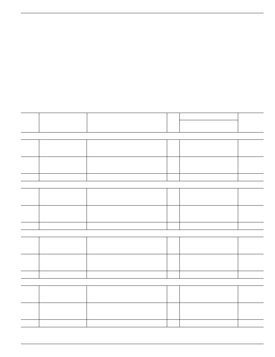
PWR GND
2
NC
3
NC
4
NC
5
NC
6
NC
7
FB
8
SIG GND
24
NC
23
NC
22
NC
21
NC
20
NC
19
NC
18
OUTPUT
17
OUTPUT
24-LEAD SOIC (WM)
9
NC
10
ON/OFF
11
NC
12
PWR GND
16
NC
15
VIN
14
VIN
13
NC
Pin Configurations
GND
5- ON/OFF
4- FEEDBACK
3- GROUND
2- OUTPUT
1- VIN
5-LEAD TO-220 (T)
GND
5- ON/OFF
4- FEEDBACK
3- GROUND
2- OUTPUT
1- VIN
5-LEAD TO-263 (U)
1
NC
2
NC
3
OUTPUT
4
NC
5
GND
6
NC
7
FB
8
NC
16
VIN
15
NC
14
GND
13
GND
12
GND
11
GND
10
NC
9
ON/OFF
16-LEAD DIP (N)
Part Number
Temperature Range
Package
LM2575BN*
≠40
∞
C to +85
∞
C
16-pin Plastic DIP
LM2575-3.3BN
≠40
∞
C to +85
∞
C
16-pin Plastic DIP
LM2575-5.0BN
≠40
∞
C to +85
∞
C
16-pin Plastic DIP
LM2575-12BN
≠40
∞
C to +85
∞
C
16-pin Plastic DIP
LM2575BWM*
≠40
∞
C to +85
∞
C
24-pin Wide SOIC
LM2575-3.3BWM
≠40
∞
C to +85
∞
C
24-pin Wide SOIC
LM2575-5.0BWM
≠40
∞
C to +85
∞
C
24-pin Wide SOIC
LM2575-12BWM
≠40
∞
C to +85
∞
C
24-pin Wide SOIC
LM2575BT*
≠40
∞
C to +85
∞
C
5-lead TO-220
LM2575-3.3BT
≠40
∞
C to +85
∞
C
5-lead TO-220
LM2575-5.0BT
≠40
∞
C to +85
∞
C
5-lead TO-220
LM2575-12BT
≠40
∞
C to +85
∞
C
5-lead TO-220
LM2575BU*
≠40
∞
C to +85
∞
C
5-lead TO-263
LM2575-3.3BU
≠40
∞
C to +85
∞
C
5-lead TO-263
LM2575-5.0BU
≠40
∞
C to +85
∞
C
5-lead TO-263
LM2575-12BU
≠40
∞
C to +85
∞
C
5-lead TO-263
* Adjustable output regulators.
Contact factory for bent or staggered leads option.
Ordering Information
August 1999
3
M2575
LM2575
Micrel
Electrical Characteristics
Specifications with standard typeface are for T
J
= 25
∞
C, and those with boldface type apply
over full Operating Temperature Range. Unless otherwise specified, V
IN
= 12V, and I
LOAD
= 200mA.
LM2575
Symbol
Parameter
Conditions
Typ
Limit
Units
(Note 2)
(Limits)
SYSTEM PARAMETERS, ADJUSTABLE REGULATORS (Note 3) Test Circuit
Figure 1
V
OUT
Feedback Voltage
V
IN
= 12V , I
LOAD
= 0.2A
1.230
V
V
OUT
= 5V
1.217
V(min)
1.243
V(max)
V
OUT
Feedback Voltage
0.2A
I
LOAD
1A, 8V
V
IN
40V
1.230
V
LM2575
V
OUT
= 5V
1.193/1.180
V(min)
1.267/1.280
V(max)
Efficiency
V
IN
= 12V, I
LOAD
= 1A, V
OUT
= 5V
82
%
SYSTEM PARAMETERS, 3.3V REGULATORS (Note 3) Test Circuit
Figure 1
V
OUT
Output Voltage
V
IN
= 12V , I
LOAD
= 0.2A
3.3
V
V
OUT
= 3.3V
3.234
V(min)
3.366
V(max)
V
OUT
Output Voltage
0.2A
I
LOAD
1A, 8V
V
IN
40V
3.3
V
LM2575-3.3
V
OUT
= 3.3V
3.168/3.135
V(min)
3.432/3.465
V(max)
Efficiency
V
IN
= 12V, I
LOAD
= 1A
75
%
SYSTEM PARAMETERS, 5V REGULATORS (Note 3) Test Circuit
Figure 1
V
OUT
Output Voltage
V
IN
= 12V , I
LOAD
= 0.2A
5.0
V
V
OUT
= 5V
4.900
V(min)
5.100
V(max)
V
OUT
Output Voltage
0.2A
I
LOAD
1A, 8V
V
IN
40V
5.0
V
LM2575-5.0
V
OUT
= 5V
4.800/4.750
V(min)
5.200/5.250
V(max)
Efficiency
V
IN
= 12V, I
LOAD
= 1A
82
%
SYSTEM PARAMETERS, 12V REGULATORS (Note 3) Test Circuit
Figure 1
V
OUT
Output Voltage
V
IN
= 25V , I
LOAD
= 0.2A
12
V
V
OUT
= 12V
11.760
V(min)
12.240
V(max)
V
OUT
Output Voltage
0.2A
I
LOAD
1A, 15V
V
IN
40V
12
V
LM2575-12
V
OUT
= 12V
11.520/11.400
V(min)
12.480/12.600
V(max)
Efficiency
V
IN
= 25V, I
LOAD
= 1A
88
%
Absolute Maximum Ratings
(Note 1)
Maximum Supply Voltage
45V
ON/OFF Pin Input Voltage
≠0.3V
V
+40V
Output Voltage to Ground (Steady State)
≠1V
Power Dissipation
Internally Limited
Storage Temperature Range
≠65
∞
C to +150
∞
C
Minimum ESD Rating
C = 100pF, R = 1.5k
2 kV
FB Pin
1 kV
Lead Temperature (soldering, 10 sec.)
260
∞
C
Maximum Junction Temperature
150
∞
C
Operating Ratings
Temperature Range
≠40
∞
C
T
J
+125
∞
C
Supply Voltage
40V
LM2575
4
August 1999
LM2575
Micrel
Electrical Characteristics (continued)
LM2575
Units
Symbol
Parameter
Conditions
Typ
Limit
(Limits)
(Note 2)
DEVICE PARAMETERS, ADJUSTABLE REGULATOR
I
B
Feedback Bias Current
V
OUT
= 5V
50
100/500
nA
DEVICE PARAMETERS, FIXED and ADJUSTABLE REGULATORS
f
O
Oscillator Frequency
52
kHz
47/42
kHz (min)
58/63
kHz (max)
V
SAT
Saturation Voltage
I
OUT
= 1A (Note 4)
0.9
V
1.2/1.4
V(max)
DC
Max Duty Cycle (ON)
(Note 5)
98
%
93
%(min)
I
CL
Current Limit
Peak Current, t
ON
3
µ
s (Note 4)
2.2
A
1.7/1.3
A(min)
3.0/3.2
A(max)
I
L
Output Leakage Current
V
IN
= 40V, (Note 6),
Output = 0V
2
mA(max)
Output = ≠1V
7.5
mA
(Note 6)
Output = ≠1V
30
mA(max)
I
Q
Quiescent Current
(Note 6)
5
mA
10
mA(max)
I
STBY
Standby Quiescent
ON/OFF Pin = 5V (OFF)
50
µ
A
Current
200
µ
A(max)
JA
Thermal Resistance
T Package, Junction to Ambient (Note 7)
65
∞
C/W
JA
T Package, Junction to Ambient (Note 8)
45
JC
T Package, Junction to Case
2
JA
N Package, Junction to Ambient (Note 9)
85
JA
WM Package, Junction to Amb. (Note 9)
100

August 1999
5
M2575
LM2575
Micrel
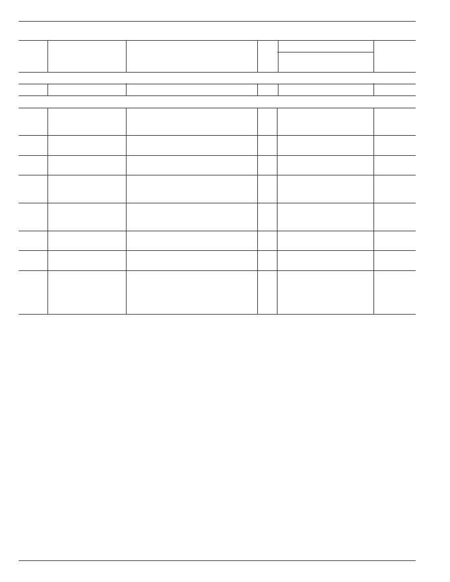
Typical Performance Characteristics
Normalized
Feedback Voltage*
JUNCTION TEMPERATURE (∞C)
NORMALIZED FEEDBACK VOLTAGE (mV)
25
20
15
10
5
0
-5
-10
-15
-20
-25
-75 -50 -25 0
25 50 75 100 125 150
VIN = 12V
ILOAD = 200mA
Normalized to TJ = 25∞C
Feedback Voltage
vs Duty Cycle*
DUTY CYCLE (%)
FEEDBACK VOLTAGE CHANGE (mV)
20
15
10
5
0
-5
-10
-15
-20
ILOAD = 200 mA
VIN = 40V
VIN = 7V
0
20
40
60
80
100
* Adjustable version only
LM2575
Units
Symbol
Parameter
Conditions
Typ
Limit
(Limits)
(Note 2)
ON/OFF CONTROL, FIXED and ADJUSTABLE REGULATORS Test Circuit
Figure 1
V
IH
ON/OFF Pin Logic
V
OUT
= 0V
1.4
2.2/2.4
V(min)
V
IL
Input Level
V
OUT
= 5V
1.2
1.0/0.8
V(max)
I
IH
ON /OFF Pin Logic
ON /OFF Pin = 5V (OFF)
4
µ
A
Current
30
µ
A(max)
I
IL
ON/OFF Pin = 0V (ON)
0.01
µ
A
10
µ
A(max)
Note 1:
Absolute Maximum Rating indicate limits beyond which damage to the device may occur. Operating Ratings indicate conditions for which the device
is intended to be functional, but do not guarantee specific performance limits. For guaranteed specifications and test conditions, see the Electrical
Characteristics.
Note 2:
All limits guaranteed at room temperature (standard type face) and at temperature extremes (bold type face) . All room temperature limits are
100% production tested. All limits at temperature extreme are guaranteed via testing.
Note 3:
External components such as the catch diode, inductor, input and output capacitors can affect switching regulator system performance. When the
LM2575/LM1575 is used as shown in
Figure 1 test circuit, system performance will be shown in system parameters section of Electrical
Characteristics.
Note 4:
Output (pin 2) sourcing current. No diode, inductor or capacitor connected to output.
Note 5:
Feedback (pin 4) removed from output and connected to 0V.
Note 6:
Feedback (pin 4) removed from output and connected to 12V to force the output transistor OFF.
Note 7:
Junction to ambient thermal resistance (no external heat sink) for the 5-lead TO-220 package mounted vertically, with 1/2" leads in a socket, or
on PC board with minimum copper area.
Note 8:
Junction to ambient thermal resistance (no external heat sink) for the 5-lead TO-220 package mounted vertically, with 1/4" leads soldered to PC
board containing approximately 4 square inches of copper area surrounding the leads.
Note 9:
Junction to ambient thermal resistance with approximately 1 square inch of pc board copper surrounding the leads. Additional copper will lower
thermal resistance further.