 | –≠–ª–µ–∫—Ç—Ä–æ–Ω–Ω—ã–π –∫–æ–º–ø–æ–Ω–µ–Ω—Ç: LMC7101B | –°–∫–∞—á–∞—Ç—å:  PDF PDF  ZIP ZIP |
September 1999
1
LMC7101
LMC7101
Micrel
LMC7101
Low-Power Operational Amplifier
General Description
The LMC7101 is a high-performance, low-power, operational
amplifier which is pin-for-pin compatible with the National
Semiconductor LMC7101. It features rail-to-rail input and
output performance in Micrel's IttyBitty
TM
SOT-23-5 package.
The LMC7101 is a 500kHz gain bandwidth amplifier de-
signed to operate from 2.7V to 12V single-ended power
supplies with guaranteed performance at supply voltages of
2.7V, 3V, 5V, and 12V.
This op amp's input common-mode range includes ground
and extends 300mV beyond the supply rails. For example,
the common-mode range is ≠0.3V to +5.3V with a 5V supply.
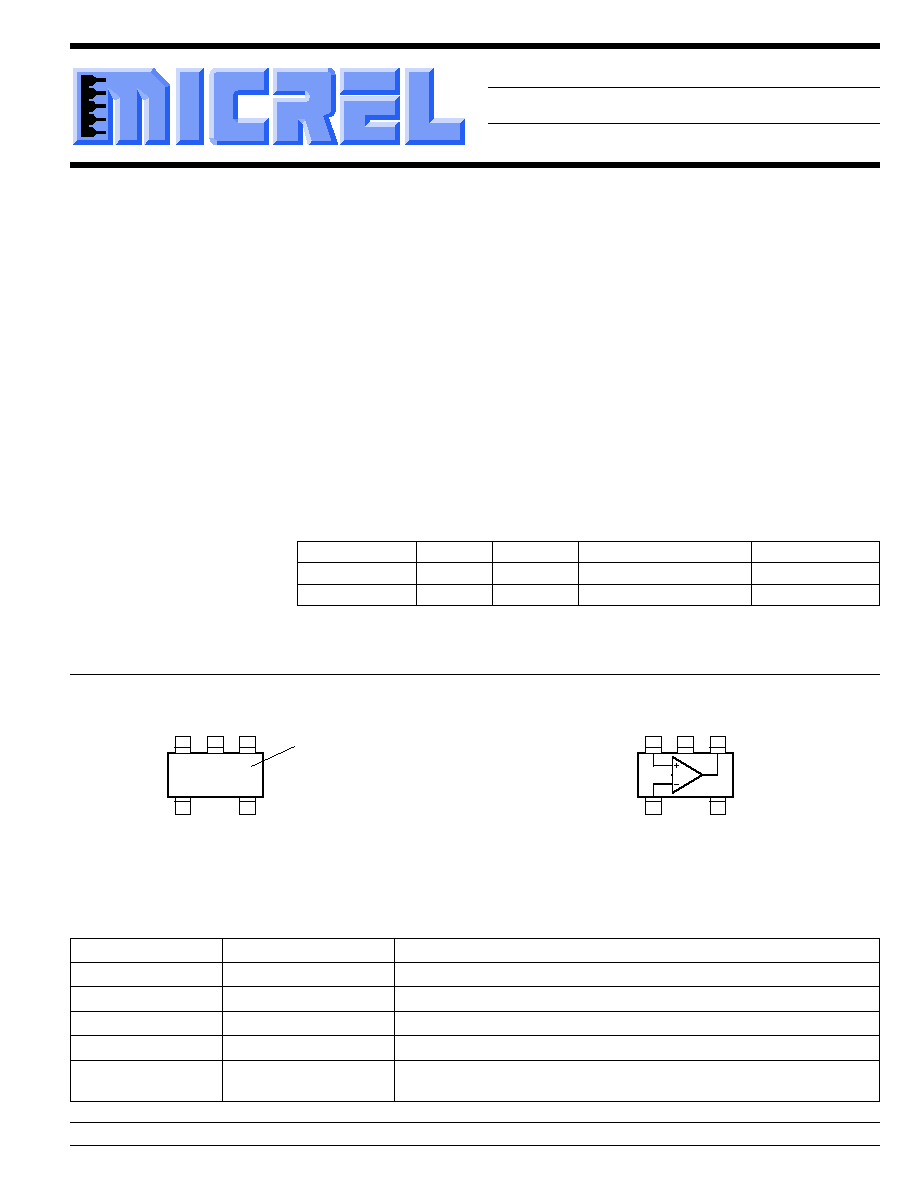
Functional Configuration
OUT
V+
IN≠
IN+
1
3
4
5
2
V≠
SOT-23-5 (M5)
Pin Description
Pin Number
Pin Name
Pin Function
1
OUT
Amplifier Output
2
V+
Positive Supply
3
IN+
Noninverting Input
4
IN≠
Inverting Input
5
V≠
Negative Supply: Negative supply for split supply application or ground for
single supply application.
Micrel, Inc. ∑ 1849 Fortune Drive ∑ San Jose, CA 95131 ∑ USA ∑ tel + 1 (408) 944-0800 ∑ fax + 1 (408) 944-0970 ∑ http://www.micrel.com
Pin Configuration
OUT
V+
IN≠
IN+
1
3
4
5
2
V≠
A12
A
Part
Identification
Ordering Information
Part Number
Marking
Grade
Temperature Range
Package
LMC7101AIM5
A12A
Prime
≠40
∞
C to +85
∞
C
SOT-23-5
LMC7101BIM5
A12
Standard
≠40
∞
C to +85
∞
C
SOT-23-5
Features
∑ Small footprint SOT-23-5 package
∑ Guaranteed 2.7V, 3V, 5V, and 12V performance
∑ 500kHz gain-bandwidth
∑ 0.01% total harmonic distortion at 10kHz (5V, 2k
)
∑ 0.5mA typical supply current at 5V
Applications
∑ Mobile communications, cellular phones, pagers
∑ Battery-powered instrumentation
∑ PCMCIA, USB
∑ Portable computers and PDAs
LMC7101
Micrel
LMC7101
2
September 1999
Electrical Characteristics (2.7V)
V+ = +2.7V, V≠ = 0V, V
CM
= V
OUT
= V+/2; R
L
= 1M
; T
J
= 25
∞
C, bold values indicate ≠40
∞
C
T
J
+85
∞
C; unless noted
LMC7101A
LMC7101B
Symbol
Parameter
Condition
Typ
Min
Max
Min
Max
Units
V
OS
Input Offset Voltage
0.11
6
9
mV
TCV
OS
Input Offset Voltage Average Drift
1.0
µ
V/
∞
C
I
B
Input Bias Current
1.0
64
64
pA
I
OS
Input Offset Current
0.5
32
32
pA
R
IN
Input Resistance
>1
T
CMRR
Common-Mode Rejection Ratio
0V
V
CM
2.7V, Note 6
70
50
50
dB
V
CM
Input Common-Mode Voltage
input low, CMRR
50dB
≠0.3
0.0
0.0
V
input high, CMRR
50dB
3.0
2.7
2.7
V
PSRR
Power Supply Rejection Ratio
V+ = 1.35V to 1.65V, V≠ =
60
50
45
dB
≠1.35V to ≠1.65V, V
CM
= 0
C
IN
Common-Mode Input Capacitance
3
pF
V
O
Output Swing
output high, R
L
= 10k
2.699
2.64
2.64
V
output low, R
L
= 10k
0.001
0.06
0.06
V
output high, R
L
= 2k
2.692
2.6
2.6
V
output low, R
L
= 2k
0.008
0.1
0.1
V
I
S
Supply Current
V
OUT
= V+/2
0.5
0.81
0.81
mA
0.95
0.95
mA
SR
Slew Rate
0.4
V/
µ
s
GBW
Gain-Bandwidth Product
0.5
MHz
Electrical Characteristics (3.0V)
V+ = +3.0V, V≠ = 0V, V
CM
= V
OUT
= V+/2; R
L
= 1M
; T
J
= 25
∞
C, bold values indicate ≠40
∞
C
T
J
+85
∞
C; unless noted
LMC7101A
LMC7101B
Symbol
Parameter
Condition
Typ
Min
Max
Min
Max
Units
V
OS
Input Offset Voltage
0.11
4
7
mV
6
9
mV
TCV
OS
Input Offset Voltage Average Drift
1.0
µ
V/
∞
C
I
B
Input Bias Current
1.0
64
64
pA
I
OS
Input Offset Current
0.5
32
32
pA
R
IN
Input Resistance
>1
T
Absolute Maximum Ratings
(Note 1)
Supply Voltage (V
V+
≠ V
V≠
) ........................................... 15V
Differential Input Voltage (V
IN+
≠ V
IN≠
) ...........
±
(V
V+
≠ V
V≠
)
I/O Pin Voltage (V
IN
, V
OUT
), Note 2
............................................. V
V+
+ 0.3V to V
V≠
≠ 0.3V
Junction Temperature (T
J
) ...................................... +150
∞
C
Storage Temperature ............................... ≠65
∞
C to +150
∞
C
Lead Temperature (soldering, 10 sec.) ..................... 260
∞
C
ESD, Note 5 .................................................................. 2kV
Operating Ratings
(Note 1)
Supply Voltage (V
V+
≠ V
V≠
) .............................. 2.7V to 12V
Ambient Temperature (T
A
) ......................... ≠40
∞
C to +85
∞
C
Junction Temperature (T
J
) ....................... ≠40
∞
C to +125
∞
C
Max. Junction Temperature (T
J(max)
), Note 3 ......... +125
∞
C
Package Thermal Resistance (
JA
), Note 4.......... 325
∞
C/W
Max. Power Dissipation ............................................ Note 3
September 1999
3
LMC7101
LMC7101
Micrel
Electrical Characteristics--DC (5V)
V+ = +5.0V, V≠ = 0V, V
CM
= 1.5V, V
OUT
= V+/2; R
L
= 1M
; T
J
= 25
∞
C, bold values indicate ≠40
∞
C
T
J
+85
∞
C; unless noted
LMC7101A
LMC7101B
Symbol
Parameter
Condition
Typ
Min
Max
Min
Max
Units
V
OS
Input Offset Voltage
0.11
3
7
mV
5
9
mV
TCV
OS
Input Offset Voltage Average Drift
1.0
µ
V/
∞
C
I
B
Input Bias Current
1.0
64
64
pA
I
OS
Input Offset Current
0.5
32
32
pA
R
IN
Input Resistance
>1
T
CMRR
Common-Mode Rejection Ratio
0V
V
CM
5V, Note 6
82
60
60
dB
55
55
dB
V
CM
Input Common-Mode Voltage
input low, CMRR
50dB
≠0.3
≠0.20
≠0.20
V
0.00
0.00
V
input high, CMRR
50dB
5.3
5.20
5.20
V
5.00
5.00
V
+PSRR
Positive Power Supply
V+ = 5V to 12V,
82
70
65
dB
Rejection Ratio
V≠ = 0V, V
OUT
= 1.5V
65
62
dB
≠PSRR
Negative Power Supply
V+ = 0V, V≠ = ≠5V to ≠12V,
82
70
65
dB
Rejection Ratio
V
OUT
= ≠1.5V
65
62
dB
C
IN
Common-Mode Input Capacitance
3
pF
V
OUT
Output Swing
output high, R
L
= 2k
4.989
4.9
4.9
V
4.85
4.85
V
output low, R
L
= 2k
0.011
0.1
0.1
V
0.15
0.15
V
output high, R
L
= 600
4.963
4.9
4.9
V
4.8
4.8
V
output low, R
L
= 600
0.037
0.1
0.1
V
0.2
0.2
V
I
SC
Output Short Circuit Current
sourcing (V
OUT
= 0V) or
200
120
120
mA
Note 7
sinking (V
OUT
= 5V)
80
80
mA
I
S
Supply Current
V
OUT
= V+/2
0.5
0.85
0.85
mA
1.0
1.0
mA
LMC7101A
LMC7101B
Symbol
Parameter
Condition
Typ
Min
Max
Min
Max
Units
CMRR
Common-Mode Rejection Ratio
0V
V
CM
3.0V, Note 6
74
60
60
dB
V
CM
Input Common-Mode Voltage
input low, CMRR
50dB
≠0.3
0
0
V
input high, CMRR
50dB
3.3
3.0
3.0
V
PSRR
Power Supply Rejection Ratio
V+ = 1.5V to 6.0V, V≠ =
80
68
60
dB
≠1.5V to ≠6.0V, V
CM
= 0
C
IN
Common-Mode Input Capacitance
3
pF
V
OUT
Output Swing
output high, R
L
= 2k
2.992
2.9
2.9
V
output low, R
L
= 2k
0.008
0.1
0.1
V
output high, R
L
= 600
2.973
2.85
2.85
V
output low, R
L
= 600
0.027
0.15
0.15
V
I
S
Supply Current
0.5
0.81
0.81
mA
0.95
0.95
mA

LMC7101
Micrel
LMC7101
4
September 1999
Electrical Characteristics--DC (12V)
V+ = +12V, V≠ = 0V, V
CM
= 1.5V, V
OUT
= V+/2; R
L
= 1M
; T
J
= 25
∞
C, bold values indicate ≠40
∞
C
T
J
+85
∞
C; unless noted
LMC7101A
LMC7101B
Symbol
Parameter
Condition
Typ
Min
Max
Min
Max
Units
V
OS
Input Offset Voltage
0.11
6
9
mV
TCV
OS
Input Offset Voltage Average Drift
1.0
µ
V/
∞
C
I
B
Input Bias Current
1.0
64
64
pA
I
OS
Input Offset Current
0.5
32
32
pA
R
IN
Input Resistance
>1
T
CMRR
Common-Mode Rejection Ratio
0V
V
CM
12V, Note 6
82
65
65
dB
60
60
dB
V
CM
Input Common-Mode Voltage
input low, V+ = 12V,
≠0.3
≠0.20
≠0.20
V
CMRR
50dB
0.00
0.00
V
input high, V+ = 12V,
12.3
12.2
12.2
V
CMRR
50dB
12.0
12.0
V
+PSRR
Positive Power Supply
V+ = 5V to 12V,
82
70
65
dB
Rejection Ratio
V≠ = 0V, V
OUT
= 1.5V
65
62
dB
≠PSRR
Negative Power Supply
V+ = 0V, V≠ = ≠5V to
82
70
65
dB
Rejection Ratio
≠12V, V
OUT
= ≠1.5V
65
62
dB
A
V
Large Signal Voltage Gain
sourcing or sinking,
340
80
80
V/mV
R
L
= 2k, Note 9
40
40
V/mV
sourcing or sinking,
300
15
15
V/mV
R
L
= 600
, Note 9
10
10
V/mV
C
IN
Common-Mode Input Capacitance
3
pF
V
OUT
Output Swing
output high, V+ = 12V,
11.98
11.9
11.9
V
R
L
= 2k
11.87
11.87
V
output low, V+ = 12V,
0.02
0.10
0.10
V
R
L
= 2k,
0.13
0.13
V
output high, V+ = 12V,
11.93
11.73
11.73
V
R
L
= 600
11.65
11.65
V
output low, V+ = 12V,
0.07
0.27
0.27
V
R
L
= 600
0.35
0.35
V
I
SC
Output Short Circuit Current
sourcing (V
OUT
= 0V) or
300
200
200
mA
sinking (V
OUT
= 12V),
120
120
mA
Notes 7, 8
I
S
Supply Current
V
OUT
= V+/2
0.8
1.5
1.5
mA
1.71
1.71
mA

September 1999
5
LMC7101
LMC7101
Micrel
Electrical Characteristics--AC (5V)
V+ = 5V, V≠ = 0V, V
CM
= 1.5V, V
OUT
= V+/2; R
L
= 1M
; T
J
= 25
∞
C, bold values indicate ≠40
∞
C
T
J
+85
∞
C; unless noted
LMC7101A
LMC7101B
Symbol
Parameter
Condition
Typ
Min
Max
Min
Max
Units
THD
Total Harmonic Distortion
f = 10kHz, A
V
= ≠2,
0.01
%
R
L
= 2k
, V
OUT
= 4.0 V
PP
SR
Slew Rate
0.3
V/
µ
s
GBW
Gain-Bandwidth Product
0.5
MHz
Electrical Characteristics--AC (12V)
V+ = 12V, V≠ = 0V, V
CM
= 1.5V, V
OUT
= V+/2; R
L
= 1M
; T
J
= 25
∞
C, bold values indicate ≠40
∞
C
T
J
+85
∞
C; unless noted
LMC7101A
LMC7101B
Symbol
Parameter
Condition
Typ
Min
Max
Min
Max
Units
THD
Total Harmonic Distortion
f = 10kHz, A
V
= ≠2,
0.01
%
R
L
= 2k, V
OUT
= 8.5 V
PP
SR
Slew Rate
V+ = 12V, Note 10
0.3
0.19
0.19
V/
µ
s
0.15
0.15
V/
µ
s
GBW
Gain-Bandwidth Product
0.5
MHz
m
Phase Margin
45
∞
G
m
Gain Margin
10
dB
e
n
Input-Referred Voltage Noise
f = 1kHz, V
CM
= 1V
37
nV/ Hz
i
n
Input-Referred Current Noise
f = 1kHz
1.5
fA/ Hz
General Notes: Devices are ESD protected; however, handling precautions are recommended. All limits guaranteed by testing on statistical analysis.
Note 1.
Absolute maximum ratings indicate limits beyond which damage to the component may occur. Electrical specifications do not apply when
operating the device outside its recommended operating ratings.
Note 2.
I/O Pin Voltage is any external voltage to which an input or output is referenced.
Note 3.
The maximum allowable power dissipation is a function of the maximum junction temperature, T
J(max)
; the junction-to-ambient thermal
resistance,
JA
; and the ambient temperature, T
A
. The maximum allowable power dissipation at any ambient temperature is calculated using:
P
D
= (T
J(max)
≠ T
A
)
˜
JA
. Exceeding the maximum allowable power dissipation will result in excessive die temperature.
Note 4.
Thermal resistance,
JA
, applies to a part soldered on a printed-circuit board.
Note 5.
Human body model, 1.5k in series with 100pF.
Note 6.
Common-mode performance tends to follow the typical value. Minimum value limits reflect performance only near the supply rails.
Note 7.
Continuous short circuit may exceed absolute maximum T
J
under some conditions.
Note 8.
Shorting OUT to V+ when V+ > 12V may damage the device.
Note 9.
R
L
connected to 5.0V. Sourcing: 5V
V
OUT
12V. Sinking: 2.5V
V
OUT
5V.
Note 10. Device connected as a voltage follower with a 12V step input. The value is the positive or negative slew rate, whichever is slower.
LMC7101
Micrel
LMC7101
6
September 1999
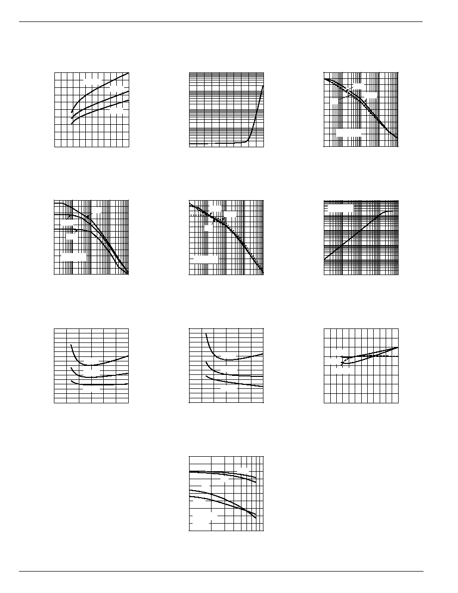
0
200
400
600
800
1000
0
2
4
6
8
10
12
SUPPLY CURRENT (
µ
A)
SUPPLY VOLTAGE (V)
Supply Current
vs. Supply Voltage
≠40
∞
C
25
∞
C
85
∞
C
1
10
100
1000
10000
-40
0
40
80
120
160
INPUT CURRENT (pA)
JUNCTION TEMPERATURE (
∞
C)
Input Current vs.
Junction Temperature
-20
0
20
40
60
80
100
1x10
1
1x10
2
1x10
3
1x10
4
1x10
5
-PSRR (dB)
FREQUENCY (Hz)
-
PSRR
vs. Frequency
5V
12V
2.7V
T
A
= 25
∞
C
0
20
40
60
80
100
120
1x10
1
1x10
2
1x10
3
1x10
4
1x10
5
+PSRR (dB)
FREQUENCY (Hz)
+
PSRR
vs. Frequency
2.7V
5V
12V
T
A
= 25
∞
C
0.01
0.1
1
10
100
1000
0.001
0.01
0.1
1
10
CURRENT SINK / SOURCE (mA)
OUTPUT VOLTAGE (V)
Sink / Source Currents
vs. Output Voltage
T
A
= 25∞C
Typical Characteristics
0
20
40
60
80
100
120
140
1x10
1
1x10
2
1x10
3
1x10
4
1x10
5
CMRR (dB)
FREQUENCY (Hz)
CMRR
vs. Frequency
2.7V
12V
5V
T
A
= 25
∞
C
0
0.1
0.2
0.3
0.4
0.5
0.6
0.7
0.8
0
2
4
6
8
10
12
SLEW RATE (V/
µ
s)
SUPPLY VOLTAGE (V)
Falling Slew Rate vs.
vs. Supply Voltage
+85
∞
C
+25
∞
C
-40
∞
C
0
0.1
0.2
0.3
0.4
0.5
0.6
0.7
0.8
0
2
4
6
8
10
12
SLEW RATE (V/
µ
s)
SUPPLY VOLTAGE (V)
Rising Slew Rate vs.
vs. Supply Voltage
+85
∞
C
-40
∞
C
+25
∞
C
0
200
400
600
800
0
2
4
6
8
10
12
OFFSET VOLTAGE (
µ
V)
SUPPLY VOLTAGE (V)
Offset Voltage
vs. Supply Voltage
25
∞
C
-40
∞
C
85
∞
C
0
20
40
60
80
100
100
1000
PHASE MARGIN (
∞
)
LOAD CAPACITANCE (pF)
Phase Margin
vs. Capacitive Load
T
A
= 25
∞
C
A
V
= 1
12V
5V
3V
2.7V
200
300
500
September 1999
7
LMC7101
LMC7101
Micrel
0
20
40
60
80
1x10
2
1x10
3
1x10
4
1x10
5
GAIN (dB)
FREQUENCY (Hz)
5V Open-Loop
Frequency Response
T
A
= 25
∞
C
1M
600
2k
-20
0
20
40
60
80
100
-60
-30
0
30
60
90
120
1x10
2
1x10
3
1x10
4
1x10
5
1x10
6
OFFSET VOLTAGE (
µ
V)
PHASE (
∞
)
COMMON-MODE VOLTAGE (V)
5V Open-Loop
Gain and Phase
100pF (
∞
)
500pF (
∞
)
1000pF (
∞
)
100pF (dB)
500pF (dB)
1000pF (dB)
T
A
= 25
∞
C
R
L
= 1M
0
20
40
60
80
100
1x10
2
1x10
3
1x10
4
1x10
5
GAIN (dB)
FREQUENCY (Hz)
2.7V Open-Loop
Frequency Response
R
L
= 1M
R
L
= 2k
T
A
= 25
∞
C
-25
0
25
50
75
100
-90
-45
0
45
90
135
1x10
2
1x10
3
1x10
4
1x10
5
1x10
6
GAIN (dB)
PHASE (
∞
)
FREQUENCY (Hz)
2.7V Open-Loop Gain
and Phase
100pF (dB)
500pF
100pF (
∞
)
500pF (
∞
)
T
A
= 25
∞
C
(dB)
R
L
= 1M
0
20
40
60
80
1x10
2
1x10
3
1x10
4
1x10
5
GAIN (dB)
FREQUENCY (Hz)
12V Open-Loop
Frequency Response
1M
600
2k
T
A
= 25
∞
C
-20
0
20
40
60
80
100
120
-60
-30
0
30
60
90
120
150
1x10
2
1x10
3
1x10
4
1x10
5
1x10
6
GAIN (dB)
PHASE (
∞
)
FREQUENCY (Hz)
12V Open-Loop Gain
and Phase
100pF (
∞
)
500pF (
∞
)
1000pF (
∞
)
100pF (dB)
500pF (dB)
1000pF (dB)
T
A
= 25
∞
C
R
L
= 1M
LMC7101
Micrel
LMC7101
8
September 1999
Inverting Small-Signal
Pulse Response
OUTPUT
INPUT
Inverting Large-Signal
Pulse Response
OUTPUT
INPUT
Noninverting Small-Signal
Pulse Response
OUTPUT
INPUT
Noninverting Large-Signal
Pulse Response
OUTPUT
INPUT
Input Voltage Noise vs. Frequency
Functional Characteristics
September 1999
9
LMC7101
LMC7101
Micrel
Application Information
Input Common-Mode Voltage
Some amplifiers exhibit undesirable or unpredictable perfor-
mance when the inputs are driven beyond the common-mode
voltage range, for example, phase inversion of the output
signal. The LMC7101 tolerates input overdrive by at least
200mV beyond either rail without producing phase inversion.
If the absolute maximum input voltage (700mV beyond either
rail) is exceeded, the input current should be limited to
±
5mA
maximum to prevent reducing reliability. A 10k
series input
resistor, used as a current limiter, will protect the input
structure from voltages as large as 50V above the supply or
below ground. See Figure 1.
V
IN
V
OUT
10k
R
IN
Figure 1. Input Current-Limit Protection
Output Voltage Swing
Sink and source output resistances of the LMC7101 are
equal. Maximum output voltage swing is determined by the
load and the approximate output resistance. The output
resistance is:
R
V
I
OUT
DROP
LOAD
=
V
DROP
is the voltage dropped within the amplifier output
stage. V
DROP
and I
LOAD
can be determined from the V
O
(output swing) portion of the appropriate Electrical Character-
istics table. I
LOAD
is equal to the typical output high voltage
minus V+/2 and divided by R
LOAD
. For example, using the
Electrical Characteristics DC (5V) table, the typical output
high voltage using a 2k
load (connected to V+/2) is 4.989V,
which produces an I
LOAD
of
1 245
4 989
2 5
2
1 245
.
.
.
.
mA
V ≠ V
k
mA
=
.
Voltage drop in the amplifier output stage is:
V
DROP
= 5.0V ≠ 4.989V
V
DROP
= 0.011V
Because of output stage symmetry, the corresponding typical
output low voltage (0.011V) also equals V
DROP
. Then:
R
V
A
9
OUT
=
=
0 011
0 001245
8 8
.
.
.
Driving Capacitive Loads
Driving a capacitive load introduces phase-lag into the output
signal, and this in turn reduces op-amp system phase margin.
The application that is least forgiving of reduced phase
margin is a unity gain amplifier. The LMC7101 can typically
drive a 100pF capacitive load connected directly to the output
when configured as a unity-gain amplifier.
Using Large-Value Feedback Resistors
A large-value feedback resistor (> 500k
) can reduce the
phase margin of a system. This occurs when the feedback
resistor acts in conjunction with input capacitance to create
phase lag in the fedback signal. Input capacitance is usually
a combination of input circuit components and other parasitic
capacitance, such as amplifier input capacitance and stray
printed circuit board capacitance.
Figure 2 illustrates a method of compensating phase lag
caused by using a large-value feedback resistor. Feedback
capacitor C
FB
introduces sufficient phase lead to overcome
the phase lag caused by feedback resistor R
FB
and input
capacitance C
IN
. The value of C
FB
is determined by first
estimating C
IN
and then applying the following formula:
R
C
R
C
IN
IN
FB
FB
◊
◊
V
IN
C
FB
R
FB
V
OUT
C
IN
R
IN
Figure 2. Cancelling Feedback Phase Lag
Since a significant percentage of C
IN
may be caused by board
layout, it is important to note that the correct value of C
FB
may
change when changing from a breadboard to the final circuit
layout.

LMC7101
Micrel
LMC7101
10
September 1999
Typical Circuits
Some single-supply, rail-to-rail applications for which the
LMC7101 is well suited are shown in the circuit diagrams of
Figures 3 through 7.
R2
900k
R1
100k
V
OUT
0V to V+
V+
V
IN
2
5
1
3
4
LMC7101
0V to
V +
A
V
Figure 3a. Noninverting Amplifier
0
100
0
100
V
OUT
(V)
V
IN
(V)
V+
A = 1 +
R2
R
10
V
1
Figure 3b. Noninverting Amplifier Behavior
V
OUT
0V to V+
V+
V
IN
0V to V+
2
5
1
3
4
LMC7101
V
OUT
= V
IN
Figure 4. Voltage Follower
V
OUT
0V to V+
V+
V
IN
0V to 2V
2
5
1
3
4
LMC7101
R
S
10
1
/
2
W
Load
V
S
0.5V to Q1 V
CEO(sus)
I
OUT
Q1
2N3904
V
CEO
= 40V
I
C(max)
= 200mA
{
Change Q1 and R
S
for higher current
and/or different gain.
I
V
R
100mA/V as shown
OUT
IN
S
=
=
Figure 5. Voltage-Controlled Current Sink
V+
0V
R4
100k
R4
100k
R3
100k
V
OUT
V+
2
5
1
4
3
LMC7101
C1
0.001µF
R2
100k
V+
Figure 6. Square Wave Oscillator
R3
330k
R1
33k
0V
R2
330k
R4
330k
C1
1µF
V
OUT
V+
2
5
1
4
3
LMC7101
C
IN
V+
C
OUT
R
L
A
R2
R1
330k
33k
10
V
= -
=
= -
Figure 7. AC-Coupled Inverting Amplifier

September 1999
11
LMC7101
LMC7101
Micrel
Package Information
0.20 (0.008)
0.09 (0.004)
0.60 (0.024)
0.10 (0.004)
3.02 (0.119)
2.80 (0.110)
10
∞
0
∞
3.00 (0.118)
2.60 (0.102)
1.75 (0.069)
1.50 (0.059)
0.95 (0.037) REF
1.30 (0.051)
0.90 (0.035)
0.15 (0.006)
0.00 (0.000)
DIMENSIONS:
MM (INCH)
0.50 (0.020)
0.35 (0.014)
1.90 (0.075) REF
SOT-23-5 (M5)

LMC7101
Micrel
LMC7101
12
September 1999
MICREL INC.
1849 FORTUNE DRIVE
SAN JOSE, CA 95131
USA
TEL
+ 1 (408) 944-0800
FAX
+ 1 (408) 944-0970
WEB
http://www.micrel.com
This information is believed to be accurate and reliable, however no responsibility is assumed by Micrel for its use nor for any infringement of patents or
other rights of third parties resulting from its use. No license is granted by implication or otherwise under any patent or patent right of Micrel Inc.
© 1999 Micrel Incorporated