P
RODUCTION
D
ATASHEET
Microsemi
Integrated Products
11861 Western Avenue, Garden Grove, CA. 92841, 714-898-8121, Fax: 714-893-2570
Page 1
Copyright
2002
Rev. 1.0, 2003-10-14
WWW
.
Microse
m
i
.
CO
M
P
P
a
a
n
n
e
e
l
l
M
M
a
a
t
t
c
c
h
h
TM
TM
LXM1643-12-62
12V Quad 6W CCFL Programmable Inverter Module
I N T E G R A T E D P R O D U C T S
D E S C R I P T I O N
The LXM1643-12-62 is a Quad 6W
Output Direct DriveTM CCFL (Cold
Cathode Fluorescent Lamp) Inverter
Module specifically designed for driving
LCD backlight lamps. It is ideal for
driving typical 12.1" to 18.1" TFT panels.
LXM1643 modules provides the
designer with a vastly superior display
brightness range then typical with analog
(amplitude control) dimming.
The inverter includes a dimming input
that permits brightness control from either
a DC voltage source or a PWM signal or
external Potentiometer. The maximum
output current is externally programmable
over a range of 5 to 8mA in 1mA steps to
allow the inverter to properly match to a
wide array of LCD panel lamp current
specifications.
RangeMAX Digital Dimming
Technique provides flicker-free brightness
control in any wide range typically (50:1+)
dimming application.
The resultant "burst drive" that
energizes the lamp was designed
specifically to ensure that no premature
lamp degradation occurs, while allowing
significant power savings at lower dim
levels.
The modules convert DC voltage from
the system battery or AC adapter directly
to high frequency, high-voltage waves
required to ignite and operate CCFL
lamps.
The LXM1643-12-62 inverter is
intended for panel assemblies with
individual lamp connections, or where
lamps are spaced apart from each other.
The LXM1643-12-61 inverter should be
used for panel applications where lamp
pairs are in close proximity and share a
common return (low side) wire.
Other benefits of this new topology
are stable fixed-frequency operation,
secondary-side strike-voltage regulation
and both open/shorted lamp protection
with fault timeout.
IMPORTANT:
For the most current data, consult
MICROSEMI
's website: http://www.microsemi.com
K E Y F E A T U R E S
Externally Programmable
Maximum Output Current
Easy to Use Brightness
Control
RangeMAX Wide Range
Dimming
Output Short-Circuit Protection
and Automatic Strike-Voltage
Regulation and Timeout
Fixed Frequency Operation
Rated From -20 to 70∞C
UL 60950 E175910
A P P L I C A T I O N S
High Brightness Displays
Desktop Displays
Industrial Display Controls
B E N E F I T S
Smooth, Flicker Free 2%-
100% Full-Range Brightness
Control
Programmable output
current allows inverter to
mate with a wide variety of
LCD panel specifications
P R O D U C T H I G H L I G H T
Universal Dimming Input PWM, VDC, or Potentiometer
DC Voltage
Source
Potentiometer
PWM
Signal
Selectable Maximum Output Current 5mA to 8mA
RMS
P A C K A G E O R D E R I N F O
P
ART
N
UMBER
O
UTPUT
C
ONNECTORS
I
NVERTER
M
ATES
D
IRECTLY TO
P
ANEL
C
ONNECTORS
LXM1643-12-62 Four
JST
SM02B-BHSS-1-TB JST
BHSR-02VS-1
L
L
X
X
M
M
1
1
6
6
4
4
3
3
-
-
1
1
2
2
-
-
6
6
2
2
P
RODUCTION
D
ATASHEET
Microsemi
Integrated Products
11861 Western Avenue, Garden Grove, CA. 92841, 714-898-8121, Fax: 714-893-2570
Page 2
Copyright
2002
Rev. 1.0, 2003-10-14
WWW
.
Microse
m
i
.
CO
M
P
P
a
a
n
n
e
e
l
l
M
M
a
a
t
t
c
c
h
h
TM
TM
LXM1643-12-62
12V Quad 6W CCFL Programmable Inverter Module
I N T E G R A T E D P R O D U C T S
A B S O L U T E M A X I M U M R A T I N G S
( N O T E 1 )
Input Signal Voltage (V
IN1
).....................................................................................................................................-0.3V to 15V
Input Power ....................................................................................................................................................................... 30W
Output Voltage, no load ............................................................................................................ Internally Limited to 2000V
RMS
Output Current (each output) ......................................................................................................9.5mA
RMS
(Internally Limited)
Output Power (each output) ............................................................................................................................................. 6.0W
Input Signal Voltage ( SLEEP Input)..................................................................................................................... -0.3V to V
IN1
Input Signal Voltage (BRITE) ...............................................................................................................................-0.3V to 5.5V
Ambient Operating Temperature, zero airflow.....................................................................................................-20∞C to 70∞C
Storage Temperature Range...............................................................................................................................-40∞C to 85∞C
Note 1: Exceeding these ratings could cause damage to the device. All voltages are with respect to Ground. Currents are positive into, negative out of specified
terminal.
R E C O M M E N D E D O P E R A T I N G C O N D I T I O N S ( R . C . )
This module has been designed to operate over a wide range of input and output conditions. However, best efficiency and performance
will be obtained if the module is operated under the condition listed in the `R.C.' column. Min. and Max. columns indicate values beyond
which the inverter, although operational, will not function optimally.
Recommended Operating Conditions
Parameter
Symbol
Min R.C. Max
Units
Input Supply Voltage Range (Fully Regulated
Lamp Current)
10.8 12 13.2
Input Supply Voltage Range (Functional)
V
IN1
10.2 12 13.8
V
Output Power (each output)
P
O
5.0
6.0* W
Linear BRITE Control Input Voltage Range
V
BRT_ADJ
0.5 2.0 V
Lamp Operating Voltage
V
LAMP
530 625 730 V
RMS
Lamp Current (Full Brightness)
I
OLAMP
5
8 mA
RMS
Operating Ambient Temperature Range
T
A
-20 70 ∞C
*Total output power must not exceed 6W . Higher voltage lamps may require maximum output current to be set lower than 8mA
RMS
E L E C T R I C A L C H A R A C T E R I S T I C S
Unless otherwise specified, the following specifications apply over the recommended operating condition and ambient temperature of
25
∞C except where otherwise noted.
LXM1643-12-62
Parameter Symbol Test
Conditions
Min Typ Max
Units
OUTPUT PIN CHARACTERISTICS
Full Bright Lamp Current (each output)
I
L(MAX)
V
BRT_ADJ
> 2.0V
DC
,
SLEEP
> 2.0V, V
IN1
= 12V
DC
I
SET1
= Ground, I
SET2
= Ground
4.0 5 5.5
mA
RMS
Full Bright Lamp Current (each output)
I
L(MAX)
V
BRT_ADJ
> 2.0V
DC
,
SLEEP
> 2.0V, V
IN1
= 12V
DC
I
SET1
= Ground, I
SET2
= Open
5.0 6 6.6
mA
RMS
Full Bright Lamp Current (each output)
I
L(MAX)
V
BRT_ADJ
> 2.0V
DC
,
SLEEP
> 2.0V, V
IN1
= 12V
DC
I
SET1
= Open, I
SET2
= Ground
6.0 7 7.7
mA
RMS
Full Bright Lamp Current (each output)
I
L(MAX)
V
BRT_ADJ
> 2.0V
DC
,
SLEEP
> 2.0V, V
IN1
= 12V
DC
I
SET1
= Open, I
SET2
= Open
7.0 8 8.8
mA
RMS
Output Current Lamp to Lamp
Deviation
I
LL%DEV
V
BRT_ADJ
> 2.0V
DC
,
SLEEP
> 2.0V, V
IN1
= 12V
DC
I
SET1
= Open, I
SET2
= Open
3
10
%
Min. Average Lamp Current
(each output)
I
L(MIN)
V
BRT_ADJ
0.5V
DC
,
SLEEP
> 2.0V, V
IN1
= 12V
DC
I
SET1
= I
SET2
= Ground
.30
mA
RMS
Lamp Start Voltage
V
LS
-20∞C
<
T
A
< 70∞C, V
IN1
> 10.8V
DC
1500
1650
V
RMS
Operating Frequency
f
O
V
BRT_ADJ
= 2.5V
DC
,
SLEEP
> 2.0V, V
IN1
= 12V
69 72 75 kHz
Burst Frequency
f
BURST
Output Burst Frequency
269
281
279
Hz
E
E
L
L
E
E
C
C
T
T
R
R
I
I
C
C
A
A
L
L
S
S
P
RODUCTION
D
ATASHEET
Microsemi
Integrated Products
11861 Western Avenue, Garden Grove, CA. 92841, 714-898-8121, Fax: 714-893-2570
Page 3
Copyright
2002
Rev. 1.0, 2003-10-14
WWW
.
Microse
m
i
.
CO
M
P
P
a
a
n
n
e
e
l
l
M
M
a
a
t
t
c
c
h
h
TM
TM
LXM1643-12-62
12V Quad 6W CCFL Programmable Inverter Module
I N T E G R A T E D P R O D U C T S
E L E C T R I C A L C H A R A C T E R I S T I C S ( C O N T I N U E D )
Unless otherwise specified, the following specifications apply over the recommended operating condition and ambient temperature of
25
∞C except where otherwise noted.
LXM1643-12-62
Parameter Symbol Test
Conditions
Min Typ Max
Units
BRITE INPUT
V
BRT_ADJ
= 0V
DC
-300
µA
DC
Input Current
I
BRT
V
BRT_ADJ
= 3V
DC
50
µA
DC
Minimum Input for Max. Lamp Current V
BRT_ADJ
I
O(LAMP)
= Maximum Lamp Current
2.0
2.05
V
DC
Maximum Input for Min. Lamp Current V
BRT_ADJ
I
O(LAMP)
= Minimum Lamp Current
0.4
0.5
V
DC
SLEEP INPUT
RUN Mode
SLEEP
V
2.0
V
IN1
V
DC
SLEEP Mode
SLEEP
V
-0.3
0.8
V
DC
SET
1,2
INPUT
SET
1,2
Low Threshold
V
L
0.4 V
Input Current
I
SET
V
SET
0.4V
-300
µA
POWER CHARACTERISTICS
Sleep Current
I
IN(MIN)
V
IN1
= 12V
DC
,
SLEEP
< 0.8V
0.0 10 30 µA
DC
Run Current
I
RUN
V
IN1
= 12V
DC
,
SLEEP
2.0V, I
SET1
= Open
I
SET2
= Ground, V
LAMP
= 625V
RMS
1750 mA
DC
Efficiency
V
IN1
= 12V
DC
,
SLEEP
2.0V, I
SET1
= Open
I
SET2
= Ground, V
LAMP
= 625V
RMS
85 %
F U N C T I O N A L P I N D E S C R I P T I O N
C
ONN
P
IN
D
ESCRIPTION
CN1
(Molex 53261-1290) Mates with 51021-1200 housing, 50079-8100 pins. Mates with LX9508 input cable assembly
CN1-1,2,3 V
IN1
Main Input Power Supply (10.8V < V
IN1
< 13.2V)
CN1-4,5,6 GND Power
Supply
Return
CN1-7
AGND
Analog Signal Ground
CN1-8 NC
No
Connect
CN1-9
SLEEP
ON/OFF Control. (0V <
SLEEP
< 0.8 = OFF,
SLEEP
>= 2.0V = ON
CN1-10
BRITE
Brightness Control (0.5V to 2.0V
DC
). 2.0V
DC
gives maximum lamp current.
CN1-11 SET
1
SET
1
MSB Connecting this pin to ground decreases the output current (see Table 1)
CN1-12 SET
2
SET
2
LSB Connecting this pin to ground decreases the output current (see Table 1)
CN2-CN5
(JST SM02B-BHSS-1-TB)
CN2-CN5-1 V
HI1
High voltage connection to high Side of lamp. Connect to lamp terminal with shortest lead length.
DO NOT
connect to Ground.
CN2-CN5-2 V
LO
Connection to low side of lamp. Connect to lamp terminal with longer lead length.
DO NOT
connect to Ground
E
E
L
L
E
E
C
C
T
T
R
R
I
I
C
C
A
A
L
L
S
S
P
RODUCTION
D
ATASHEET
Microsemi
Integrated Products
11861 Western Avenue, Garden Grove, CA. 92841, 714-898-8121, Fax: 714-893-2570
Page 4
Copyright
2002
Rev. 1.0, 2003-10-14
WWW
.
Microse
m
i
.
CO
M
P
P
a
a
n
n
e
e
l
l
M
M
a
a
t
t
c
c
h
h
TM
TM
LXM1643-12-62
12V Quad 6W CCFL Programmable Inverter Module
I N T E G R A T E D P R O D U C T S
T A B L E 1
OUTPUT CURRENT SETTINGS
SET
1
(Pin 11)
SET
2
(Pin 12)
Nominal Output Current
Open*
Open*
8.0mA
Open*
Ground
7.0mA
Ground
Open*
6.0mA
Ground
Ground
5.0mA
* If driven by a logic signal it should be open collector or open drain only, not a voltage source.
P H Y S I C A L D I M E N S I O N S
L X M 1 6 4 3 - 1 2 - 6 2
Weight: (45g) typ
.
Warning
High Voltage Present at
high side of Transformer
and Output Connector
188mm
7.40in.
G
ROUNDED
M
OUNTING
H
OLES
3.18MM ±.08
DIA
.
36mm
1.42in.
PCB tolerances ± 0.5mm
4.7mm
0.18in.
1.7mm
0.67in.
8mm Max
0.315in.
CN-1
182mm
7.165in.
4mm
0.16in
4mm
0.16in.
4mm
0.16in
94mm
3.70in.
6mm
0.23in
SM02B-BHSS-1-TB
(JST) ◊ 4
88mm ± 0.2mm
3.645
in.
88mm ± 0.2mm
3.645
in.
28mm ± 0.2mm
1.10in.
All dimensions are in millimeters, inches are for reference only.
S I M P L I F I E D B L O C K D I A G R A M
Ram p
Gen
Output
Driver
0.5 -
2V
DC
+
-
LAM
P
V
LO
V
HI
Comparator
Ramp
V
BRITE
SET
1
High Voltage Transformers
I
SENSE
OV
SENSE
SET
2
+3V
10K
10K
+3V
+3V
V
IN1
OC
SENSE
10K
Controller
One of two
LAM
P
V
HI
Z
Z
Z
V
LO
P
P
A
A
C
C
K
K
A
A
G
G
E
E
D
D
A
A
T
T
A
A
P
RODUCTION
D
ATASHEET
Microsemi
Integrated Products
11861 Western Avenue, Garden Grove, CA. 92841, 714-898-8121, Fax: 714-893-2570
Page 5
Copyright
2002
Rev. 1.0, 2003-10-14
WWW
.
Microse
m
i
.
CO
M
P
P
a
a
n
n
e
e
l
l
M
M
a
a
t
t
c
c
h
h
TM
TM
LXM1643-12-62
12V Quad 6W CCFL Programmable Inverter Module
I N T E G R A T E D P R O D U C T S
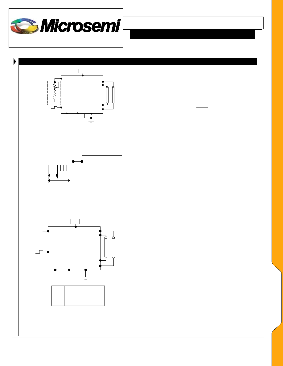
T Y P I C A L A P P L I C A T I O N
LXM1643-12-62
12V
SET
2
GND
V
Hx
V
LOx
BRITE
V
IN1
SLEEP
SET
1
0.45V
to 2.0V
1.8K
20K
DAC or
Pot
NC
NC
V
Hx
One of
two
V
LOx
Figure 1
≠ Brightness Control
(Output current set to maximum)
P.W .
10us to 125uS
BRITE
LXM1643-12-62
0 < P.W. < 100% of period
PW M Signal
from System
Figure 1A
≠ PWM Brightness Control
LXM1643-12-62
SLEEP
BRITE
12V
V
IN1
SET
2
GND
SET
1
One
of two
L L 5.0mA
RMS
L H 6.0mA
RMS
H L 7.0mA
RMS
H H 8.0mA
RMS
L=GND; H=Open
Figure 2
≠ Max Output Current
(SET
1
and SET
2
Inputs)
The brightness control may be a voltage output DAC or
other voltage source, a digital pot or 20K manual pot. The
inverter contains an internal 10K pull-up to 3V to bias the
pot add a 1.8K resistor to set the lower threshold voltage.
A 3.3V Logic Level PWM signal from a micro-controller
may also be used as shown in Figure 1A.
If you need to turn the inverter ON/OFF remotely, connect
to TTL logic signal to the
SLEEP
input.
Connect V
HI
to high voltage wire from the lamp. Connect
V
LO
to the low voltage wire (wire with thinner insulation).
Never connect V
LO
to circuit ground as this will defeat
lamp current regulation. If both lamp wires have heavy
high voltage insulation, connect the longest wire to V
LO
.
This wire is typically white.
Use the SET
1
and SET
2
(see Figure 2) inputs to select the
desired maximum output current. Using these two pins in
combination allows the inverter to match a wide variety of
panels from different manufactures. Generally the best
lamp lifetime correlates with driving the CCFL at the
manufactures nominal current setting. However the SET
1
and SET
2
inputs allow the user the flexibility to adjust the
current to the maximum allowable output current to
increase panel brightness at the expense of some reduced
lamp life.
Although the SET pins are designed such that just leaving
them open or grounding them is all that is needed to set the
output current, they can also be actively set. Using a open
collector or open drain logic signal will allow you to
reduce the lamp current for situations where greater dim
range is required, as an example in nighttime situations. In
conjunction with a light sensor or other timer the panel
could be set to higher brightness (maximum output
current) for daytime illumination and lower brightness
(minimum or typical output current) at nighttime. Since
the dim ratio is a factor of both the burst duty cycle and the
peak output current, using this technique the effective dim
ratio can be increased greater than the burst duty cycle
alone. Conversely the SET inputs could be used to
overdrive the lamp temporarily to facilitate faster lamp
warm up at initial lamp turn on. Of course any possible
degradation on lamp life from such practices is the users
responsibility since not all lamps are designed to be
overdriven.
The inverter has a built in fault timeout function. If the
output return is open (lamp disconnected or broken) or
shorted the inverter will attempt to strike the lamp for
several seconds. After about a second without success the
inverter will shutdown. In order to restart the inverter it is
necessary to toggle the sleep input or cycle the V
IN1
input
supply. In the timeout shutdown mode input drain current
will be about 8mA.
A
A
P
P
P
P
L
L
I
I
C
C
A
A
T
T
I
I
O
O
N
N

P
RODUCTION
D
ATASHEET
Microsemi
Integrated Products
11861 Western Avenue, Garden Grove, CA. 92841, 714-898-8121, Fax: 714-893-2570
Page 6
Copyright
2002
Rev. 1.0, 2003-10-14
WWW
.
Microse
m
i
.
CO
M
P
P
a
a
n
n
e
e
l
l
M
M
a
a
t
t
c
c
h
h
TM
TM
LXM1643-12-62
12V Quad 6W CCFL Programmable Inverter Module
I N T E G R A T E D P R O D U C T S
N O T E S
PRODUCTION DATA ≠ Information contained in this document is proprietary to
Microsemi and is current as of publication date. This document may not be modified in
any way without the express written consent of Microsemi. Product processing does not
necessarily include testing of all parameters. Microsemi reserves the right to change the
configuration and performance of the product and to discontinue product at any time.
N
N
O
O
T
T
E
E
S
S