 | –≠–ª–µ–∫—Ç—Ä–æ–Ω–Ω—ã–π –∫–æ–º–ø–æ–Ω–µ–Ω—Ç: MIC184BM | –°–∫–∞—á–∞—Ç—å:  PDF PDF  ZIP ZIP |

November 2000
1
MIC184
MIC184
Micrel
MIC184
Local/Remote Thermal Supervisor
Advance Information
General Description
The MIC184 is a versatile digital thermal supervisor capable
of measuring temperature using either its own internal sensor
or an inexpensive external sensor. A 2-wire serial interface is
provided to allow communication with either I
2
C or SMBus
masters. This device is a pin-for-pin and software compatible
upgrade for the industry standard LM75.
Additional features include remote temperature measure-
ment capability, and interrupt status and mask bits in the
chip's configuration register for software polling. The open-
drain interrupt output pin can be used as either an overtem-
perature alarm or thermostatic control signal. Three program-
mable address pins permit users to multidrop up to 8 devices
along the 2-wire bus, allowing simple distributed temperature
sensing networks. Superior performance, low power and
small size makes the MIC184 an excellent choice for the most
demanding thermal management applications.
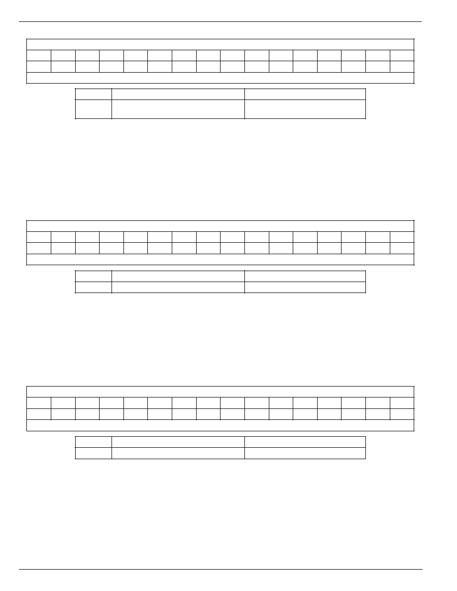
Typical Application
DATA
1
2
3
8
4
5
6
7
FROM
SERIAL BUS
HOST
OPTIONAL
REMOTE
TEMPERATURE
SENSOR
2200pF
MIC184
CLK
INT
Data
3.0V to 3.6V
V
DD
Clock
Interrupt
VDD
3
◊
10k
A2/T1
A1
A0
GND
0.1
µ
F
ceramic
2-Channel SMBus Temperature Measurement System
Features
∑ Measures local and remote temperatures
∑ Pin and software backward compatible to LM75
∑ 9-bit sigma-delta ADC
∑ 2-wire I
2
C/SMBus compatible interface
∑ Programmable thermostatic settings for either internal or
external zone
∑ Open-drain comparator/interrupt output pin
∑ Interrupt mask and status bits
∑ Low-power shutdown mode
∑ Fail-safe response to diode faults
∑ 2.7V to 5.5V power supply range
∑ Up to 8 devices may share the same bus
∑ 8-Lead SOP and MSOP Packages
Applications
∑ Desktop, Server and Notebook Computers
∑ Printers and Copiers
∑ Test and measurement equipment
∑ Consumer electronics
Ordering Information
Part Number
Temperature Range
Package
MIC184BM
≠55
∞
C to +125
∞
C
8-lead SOP
MIC184BMM
≠55
∞
C to +125
∞
C
8-lead MSOP
Micrel, Inc. ∑ 1849 Fortune Drive ∑ San Jose, CA 95131 ∑ USA ∑ tel + 1 (408) 944-0800 ∑ fax + 1 (408) 944-0970 ∑ http://www.micrel.com

MIC184
Micrel
MIC184
2
November 2000
Pin Description
Pin Number
Pin Name
Pin Function
1
DATA
Data (Digital I/O): Open-drain. Serial data input/output.
2
CLK
Clock (Digital Input): The host provides the serial bit clock on this input.
3
INT
Interrupt (Digital Output): Open-drain. Interrupt or thermostat output.
4
GND
Ground: Power and signal return for all IC functions.
5
A2/T1
Address Bit 2 (Digital Input): Slave address selection input. See "Slave
Address Truth Table."
Temperature Sensor 1 (Analog Input): Input from remote temperature sensor
(diode junction).
6
A1
Address Bit 1 (Digital Input): Slave address selection input. See "Slave
Address Truth Table."
7
A0
Address Bit 0 (Digital Input): Slave address selection input. See "Slave
Address Truth Table."
8
VDD
Supply (Analog Input): Power supply input to the IC.
Pin Configuration
1
DATA
CLK
INT
GND
8
VDD
A0
A1
A2/T1
7
6
5
2
3
4

November 2000
3
MIC184
MIC184
Micrel
Absolute Maximum Ratings
(Note 1)
Power Supply Voltage, V
DD ...................................................
6.0V
Voltage on Any Pin ................................ ≠0.3V to V
DD
+0.3V
Current Into Any Pin ...................................................
±
6mA
Power Dissipation, T
A
= +125
∞
C ............................... 30mW
Junction Temperature ............................................. +150
∞
C
Storage Temperature ............................... ≠65
∞
C to +150
∞
C
ESD Ratings (Note 3)
Human Body Model .................................................. TBD V
Machine Model ......................................................... TBD V
Soldering
Vapor Phase (60 sec.) ............................. +220
∞
C
+5
/
≠0
∞
C
Infrared (15 sec.) ...................................... +235
∞
C
+5
/
≠0
∞
C
Operating Ratings
(Note 2)
Power Supply Voltage, V
DD ..............................
+2.7V to +5.5V
Ambient Temperature Range (T
A
) ............ -55
∞
C to +125
∞
C
Package Thermal Resistance (
JA
)
SOP ................................................................. +152
∞
C/W
MSOP .............................................................. +206
∞
C/W
Electrical Characteristics
2.7V
V
DD
5.5; T
A
= +25
∞
C, bold values indicate ≠55
∞
C
T
A
+125
∞
C, Note 4; unless noted.
Symbol
Parameter
Condition
Min
Typ
Max
Units
Power Supply
I
DD
Supply Current
INT open, A2, A1, A0 = V
DD
or GND,
340
TBD
µ
A
CLK = DATA = high, normal mode
shutdown mode, CLK = 100kHz
2.5
µ
A
INT open, A2, A1, A0 = V
DD
or GND,
1
TBD
µ
A
CLK = DATA = high, shutdown mode
t
POR
Power-On Reset Time
V
DD
> V
POR
15
100
µ
s
V
POR
Power-On Reset Voltage
all registers reset to default values,
2.0
2.7
V
A/D conversions initiated
V
HYST
Power-On Reset Hysteresis Voltage
250
mV
Temperature-to-Digital Converter Characteristics
Accuracy--Local Temperature
0
∞
C
T
A
+100
∞
C, INT open,
±
1
±
2
∞
C
Note 5, 6
3V
V
DD
3.6V
≠55
∞
C
T
A
+125
∞
C, INT open,
±
2
±
3
∞
C
3V
V
DD
3.6V
Accuracy--Remote Temperature
0
∞
C
T
D
+100
∞
C, INT open,
±
1
±
3
∞
C
Note 5, 6, 7
3V
V
DD
3.6V, 0
∞
C
T
A
+85
∞
C
≠55
∞
C
T
D
+125
∞
C, INT open,
±
2
±
5
∞
C
3V
V
DD
3.6V, 0
∞
C
T
A
+85
∞
C
t
CONV
Conversion Time, Note 5
local temperature
100
160
ms
remote temperature
200
320
ms
Remote Temperature Input (T1)
I
F
Current to External Diode
high level
224
400
µ
A
Note 5
low level
7.5
14
µ
A
Address Inputs (A2/T1, A1, A0)
V
IL
Low Input Voltage
2.7V
V
DD
5.5V
0.6
V
V
IH
High Input Voltage
2.7V
V
DD
5.5V
2.0
V
C
IN
Input Capacitance
10
pF
I
LEAK
Input Current
±
0.01
±
1
µ
A
I
PD
Pulldown Current on A2/T1
A2 = V
DD
, flows for t
POR
at power-up
25
µ
A
MIC184
Micrel
MIC184
4
November 2000
Symbol
Parameter
Condition
Min
Typ
Max
Units
Serial Data I/O Pin (DATA)
V
OL
Low Output Voltage
I
OL
= 3mA
0.4
V
I
OL
= 6mA
0.8
V
V
IL
Low Input Voltage
2.7V
V
DD
5.5V
0.3V
DD
V
V
IH
High Input Voltage
2.7V
V
DD
5.5V
0.7V
DD
V
C
IN
Input Capacitance
10
pF
I
LEAK
Input current
±
0.01
±
1
µ
A
Serial Clock Input (CLK)
V
IL
Low Input Voltage
2.7V
V
DD
5.5V
0.3V
DD
V
V
IH
High Input Voltage
2.7V
V
DD
5.5V
0.7V
DD
V
C
IN
Input Capacitance
10
pF
I
LEAK
Input current
±
0.01
±
1
µ
A
Status Output (INT)
V
OL
Low Output Voltage,
I
OL
= 3mA
0.4
V
Note 8
I
OL
= 6mA
0.8
V
t
INT
Interrupt Propagation Delay,
from TEMP > T_SET, FQ = 00 to INT < V
OL
,
t
CONV
+1
µ
s
Note 5
R
PULLUP
= 10k
; POL bit = 0
t
nINT
Interrupt Reset Propagation Delay,
from any register read to INT > VOH,
1
µ
s
Note 5
R
PULLUP
= 10k
; POL bit = 0
T_SET
Default T_SET Value
t
POR
after V
DD
> V
POR
, Note 9
80
80
80
∞
C
HYST
Default HYST Value
t
POR
after V
DD
> V
POR
, Note 9
75
75
75
∞
C
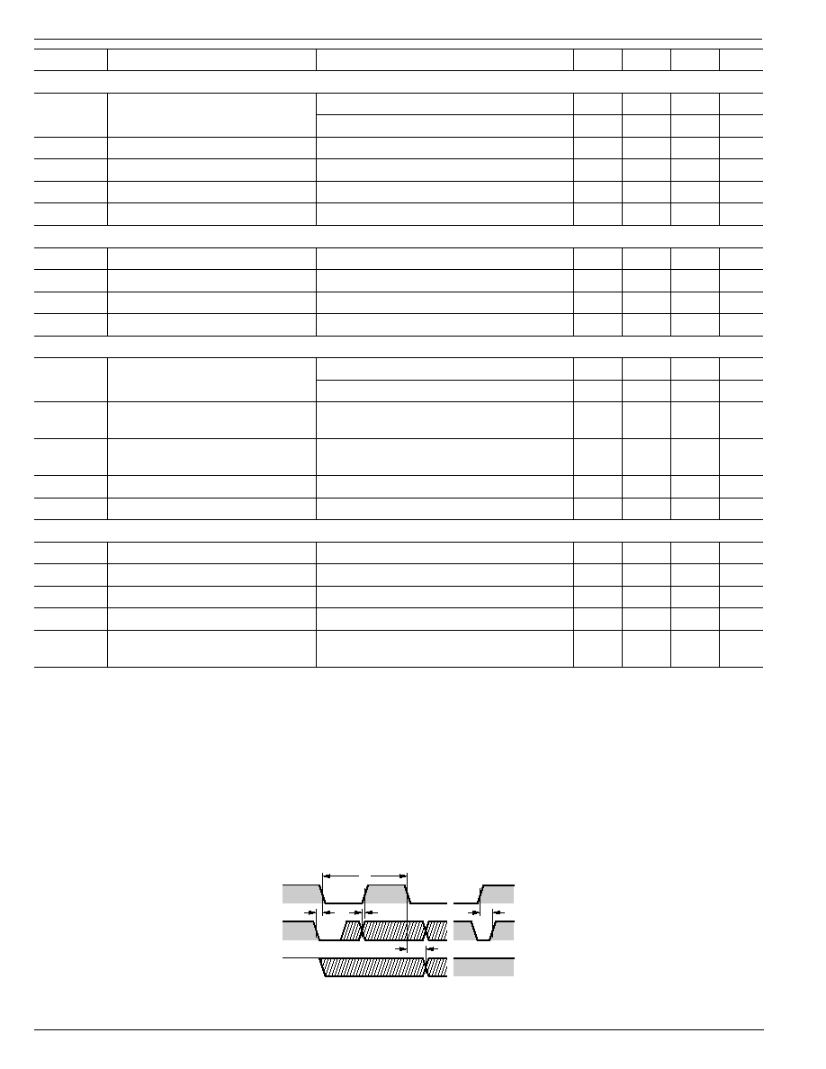
Serial Interface Timing (Note 5)
t
1
CLK (Clock) Period
2.5
µ
s
t
2
Data In Setup Time to CLK High
100
ns
t
3
Data Out Stable After CLK Low
0
ns
t
4
DATA Low Setup Time to CLK Low
start condition
100
ns
t
5
DATA High Hold Time
stop condition
100
ns
After CLK High
Note 1.
Exceeding the absolute maximum rating may damage the device.
Note 2.
The device is not guaranteed to function outside its operating rating.
Note 3.
Devices are ESD sensitive. Handling precautions recommended.
Human body model: 1.5k in series with 100pF. Machine model: 200pF, no series resistance.
Note 4.
Final test on outgoing product is performed at T
A
= TBD
∞
C.
Note 5.
Guaranteed by design over the operating temperature range. Not 100% production tested.
Note 6.
Accuracy specification does not include quantization noise, which may be as great as
±
1
/
2
LSB (
±
1
/
4
∞
C).
Note 7.
T
D
is the temperature of the remote diode junction. Testing is performed using a single unit of one of the transistors listed in Table 5.
Note 8.
Current into the INT pin will result in self-heating of the MIC184. INT pin current should be minimized for best accuracy.
Note 9.
This is the decimal representation of a binary data value.
Timing Diagram
t
1
t
2
t
5
t
4
t
3
SCL
SDA Input
SDA Output
Serial Interface Timing

November 2000
5
MIC184
MIC184
Micrel
Typical Characteristics
-3
-2
-1
0
1
2
3
-60
-40
-20
0
20
40
60
80
100
120
140
MESUREMENT ERROR (
∞
C)
LOCAL DIODE TEMERATURE (
∞
C)
Local Temperature
Measurement Error
V
DD
= 3.3V
-5
-4
-3
-2
-1
0
1
2
3
4
5
-60
-40
-20
0
20
40
60
80
100
120
140
MESUREMENT ERROR (
∞
C)
REMOTE DIODE TEMERATURE (
∞
C)
Remote Temperature
Measurement Error
V
DD
= 3.3V
0
50
100
150
200
250
300
350
400
450
500
-60
-40
-20
0
20
40
60
80
100
120
140
SUPPLY CURRENT (
µ
A)
TEMPERATURE (
∞
C)
Operating I
DD
vs. Temperature
V
DD
= 3.3V
V
DD
= 5.0V
f
CLOCK
= 0Hz
0
1
2
3
4
5
6
7
8
9
0
50 100 150 200 250 300 350 400
SHUTDOWN CURRENT (
µ
A)
CLOCK FREQUENCY (kHz)
Shutdown I
DD
vs. Frequency
V
DD
= 3.0V
V
DD
= 5.0V
0
0.5
1
1.5
2
2.5
3
3.5
-60
-40
-20
0
20
40
60
80
100
120
140
SHUTDOWN CURRENT (
µ
A)
TEMPERATURE (
∞
C)
Shutdown Mode I
DD
vs. Temperature
V
DD
= 5.0V
V
DD
= 3.3V
f
CLOCK
= 0Hz
0
50
100
150
200
250
300
350
400
0
2
4
6
QUIESCENT CURRENT (
µ
A)
SUPPLY VOLTAGE (V)
Shutdown Mode IDD
vs. Suply Voltage
0
20
40
60
80
100
120
140
0
5
10
15
MEASURED LOCAL TEMPERATURE (
∞
C)
TIME (Sec)
Response to Immersion in
125
∞
C Fluid Bath
SOIC-8
MSOP-8
-30
-25
-20
-15
-10
-5
0
5
1x10
6
1x10
7
1x10
8
1x10
9
MEASUREMENT ERROR (
∞
C)
RESISTANCE FROM T1(
)
Measurement Error vs.
PCB Leakage to +5V/+3.3V/GND
GND
3.3V
5.0V
-12
-10
-8
-6
-4
-2
0
0 1 2 3 4 5 6 7 8 9 10
MEASURMENT ERROR (
∞
C)
CAPACITANCE (nF)
Measurment Error vs.
Capcitance on T1
MIC184
Micrel
MIC184
6
November 2000
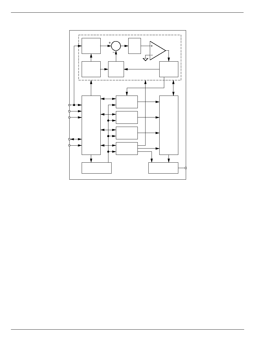
Functional Description
Pin Descriptions
VDD
Power supply input. See electrical specifications.
GND
Ground return for all MIC184 functions.
CLK
Clock input to the MIC184 from the two-wire serial bus. The
clock signal is provided by the bus host and is shared by all
devices on the bus.
DATA
Serial data I/O pin that connects to the two-wire serial bus.
DATA is bidirectional and has an open-drain output driver. An
external pull-up resistor or current source somewhere in the
system is necessary on this line. This line is shared by all
devices on the bus.
A2/T1, A1, A0
These inputs set the three least significant bits of the MIC184's
7-bit slave address. Each MIC184 will only respond to its own
unique slave address, allowing the use of up to eight MIC184s
on a single bus. A match between the MIC184's address and
Functional Diagram
2:1
MUX
TEMPERATURE-TO-DIGITAL
CONVERTER
1-Bit
DAC
A2/T1
A1
A0
DATA
MIC184
CLK
INT
2-Wire
Serial Bus
Interface
Pointer
Register
Temperature
Hysteresis
Register
State
Machine
and
Digital
Comparator
Digital Filter
and
Control
Logic
Thermostat
Output
Configuration
Register
Bandgap
Sensor
and
Reference
Result
Register
Temperature
Setpoint
Register
the address specified in the serial bit stream must be made
to initiate communication. A1 and A0 should be connected
directly to V
DD
or ground. When A2/T1 is used as an address
bit input, it should also be tied to V
DD
or ground. A2/T1 can
alternatively connect to a remote temperature sensor. When
A2/T1 is used for temperature measurements, an off-chip
diode junction must be connected between A2/T1 and ground.
In this case, internal circuitry will detect A2 as logic low,
leaving four possible slave addresses. See "Temperature
Measurement" and "Power On" for more information. A2/T1,
A1, and A0 determine the slave address as shown in Table 1.
INT
Temperature events are indicated to external circuitry via this
output. INT may be configured as active-low or active-high by
the host. Operation of the INT output is controlled by the
MODE and POL bits in the MIC184's configuration register.
See "Comparator and Interrupt Modes" below. This output is
open-drain and may be wire-ORed with other open-drain
signals. Most systems will require a pull-up resistor or current
source on this pin. If the IM bit in the configuration register is
set, it prevents the INT output from sinking current. In I
2
C and
SMBus systems, the IM bit is therefore an interrupt mask bit.

November 2000
7
MIC184
MIC184
Micrel
s
t
u
p
n
I
s
s
e
r
d
d
A
e
v
a
l
S
4
8
1
C
I
M
1
T
/
2
A
1
A
0
A
y
r
a
n
i
B
x
e
H
0
0
0
0
0
0
1
0
0
1
b
8
4
h
0
0
1
1
0
0
1
0
0
1
b
9
4
h
0
1
0
0
1
0
1
0
0
1
b
A
4
h
0
1
1
1
1
0
1
0
0
1
b
B
4
h
1
0
0
0
0
1
1
0
0
1
b
C
4
h
1
0
1
1
0
1
1
0
0
1
b
D
4
h
1
1
0
0
1
1
1
0
0
1
b
E
4
h
1
1
1
1
1
1
1
0
0
1
b
F
4
h
e
d
o
i
d
0
0
0
0
0
1
0
0
1
b
8
4
h
e
d
o
i
d
0
1
1
0
0
1
0
0
1
b
9
4
h
e
d
o
i
d
1
0
0
1
0
1
0
0
1
b
A
4
h
e
d
o
i
d
1
1
1
1
0
1
0
0
1
b
B
4
h
Table 1. MIC184 Slave Address Settings
Temperature Measurement
The temperature-to-digital converter for both internal and
external temperature data is built around a switched current
source and a 9-bit analog-to-digital converter. The tempera-
ture is calculated by measuring the forward voltage of a diode
junction at two different bias current levels. An internal
multiplexer directs the current source's output to either an
internal or external diode junction.
The MIC184 uses two's-complement data to represent tem-
peratures. If the MSB of a temperature value is 0, the
temperature is
0
∞
C. If the MSB is 1, the temperature is < 0
∞
.
More detail on this is given in "Temperature Data Format"
below. A
temperature event results if the value in the tem-
perature result register (TEMP) is greater than the value in
the overtemperature setpoint register (T_SET), or if it is less
than the value in the temperature hysteresis register
(T_HYST).
The value of the ZONE bit in the configuration register
determines whether readings are taken from the on-chip
sensor or from the A2/T1 input. At power-up, the ZONE bit of
the configuration register is set to zero. The MIC184 therefore
monitors its internal temperature and compares the result
against the contents of T_SET and T_HYST. Setting the
ZONE bit in CONFIG will result in the MIC184 acquiring
temperature data from an external diode connected to the
A2/T1 pin. This diode may be embedded in an integrated
circuit (such as a CPU, ASIC, or graphics processor), or it
may be a diode-connected discrete transistor. Once the new
value is written to CONFIG, the A/D converter will begin a new
conversion and return temperature data from the external
zone. This data will be compared against T_SET, T_HYST,
and the state of the Fault_Queue (described below). The
internal status bit (STS) and the INT output will then be
updated accordingly. See "Applications Information" for more
details on switching between zones.
Diode Faults
The MIC184 is designed to respond in a fail-safe manner to
hardware faults in the external sensing circuitry. If the con-
nection to the external diode is lost, or the sense line (A2/T1)
is shorted to V
DD
or ground, the temperature data reported by
the A/D converter will be forced to its full-scale value
(+127.5
∞
C). This will cause an overtemperature event to
occur whenever T_SET
+127.0
∞
C (0 1111 1110
b
). An
interrupt will be generated if so enabled. The temperature
reported for the external zone will remain 0 1111 1111
b
=
+127.5
∞
C until the fault condition is cleared. This fault detec-
tion requires that the MIC184 complete the number of conver-
sion cycles specified by Fault_Queue. The MIC184 may
therefore require one or more conversion cycles following
power-on or a transition from shutdown to normal operation
before reporting an external diode fault.
Serial Port Operation
The MIC184 uses standard SMBus WRITE_BYTE,
READ_BYTE, WRITE_WORD, and READ_WORD opera-
tions for communication with its host. The SMBus
WRITE_BYTE and WRITE_WORD operations involve send-
ing the device's slave address (with the R/W bit low to signal
a write operation), followed by a command byte and one or
two data bytes. The SMBus READ_BYTE operation is simi-
lar, but is a composite write and read operation: the host first
sends the device's slave address followed by the command
byte, as in a write operation. A new "start" bit must then be
sent to the MIC184, followed by a repeat of the slave address
with the R/W bit (LSB) set to the high (read) state. The data
e
t
y
B
_
d
n
a
m
m
o
C
r
e
t
s
i
g
e
R
t
e
g
r
a
T
y
r
a
n
i
B
x
e
H
l
e
b
a
L
n
o
i
t
p
i
r
c
s
e
D
0
0
0
0
0
0
0
0
b
0
0
h
P
M
E
T
t
l
u
s
e
r
e
r
u
t
a
r
e
p
m
e
t
d
e
r
u
s
a
e
m
1
0
0
0
0
0
0
0
b
1
0
h
G
I
F
N
O
C
r
e
t
s
i
g
e
r
n
o
i
t
a
r
u
g
i
f
n
o
c
0
1
0
0
0
0
0
0
b
2
0
h
T
S
Y
H
_
T
s
i
s
e
r
e
t
s
y
h
e
r
u
t
a
r
e
p
m
e
t
1
1
0
0
0
0
0
0
b
3
0
h
T
E
S
_
T
t
n
i
o
p
t
e
s
e
r
u
t
a
r
e
p
m
e
t
r
e
v
o
0
0
1
0
0
0
0
0
b
4
0
h
d
e
v
r
e
s
e
r
e
s
u
t
o
n
o
d
∑
∑
∑
∑
∑
∑
1
1
1
1
1
1
1
1
b
F
F
h
Table 2. MIC184 Register Addresses
MIC184
Micrel
MIC184
8
November 2000
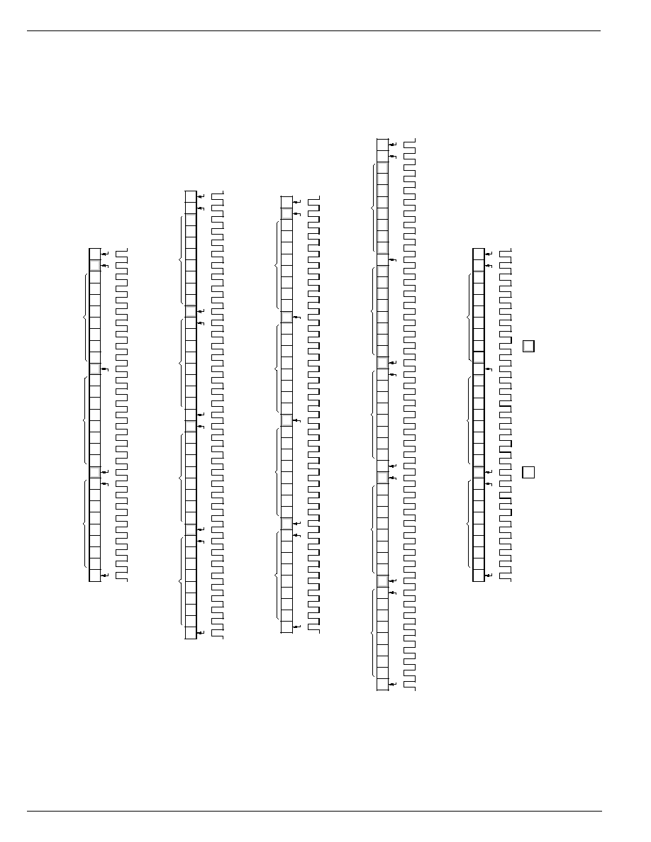
S
1001
A2
A1
A0
0
A
000000
X
X
A
D4
D5
D6
D3
D2
D1
D0
D7
/A
P
MIC184 Sla
v
e
Address
D
ATA
CLK
Command Byte
Data Byte to MIC184
ST
AR
T
ST
OP
R/W =
WRITE
A
CKNO
W
LEDGE
A
C
KNO
WLEDGE
NO
T A
C
KNO
W
LEDGE
Figure 1.
WRITE_BYTE Protocol
S
1001
A2
A1
A0
A2
A1
A0
0
A
000000
XXAS
1
1
1
00
D4
D5
D6
D3
D2
D1
D0
A
D7
/A
P
MIC184 Sla
v
e Address
D
ATA
CLK
Command Byte
MIC184 Sla
v
e Address
Data Read F
r
om MIC184
ST
AR
T
ST
AR
T
ST
OP
R/W =
WRITE
R/W = READ
A
CKNO
WLEDGE
A
CKNO
WLEDGE
A
CKNO
WLEDGE
NO
T A
CKNO
WLEDGE
Figure 2.
READ_BYTE Protocol
S
1001
A2
A1
A0
0
A
000000
X
X
A
D8
D7
D6
D5
D4
D3
D0
D1
A
D0
XXXXXXX
/
A
P
MIC184 Sla
v
e
Address
D
ATA
CLK
Command Byte
High-Order Byte to MIC184
Lo
w-Order Byte to MIC184
ST
AR
T
ST
OP
R/W =
WRITE
A
CKNO
WLEDGE
A
CKNO
WLEDGE
A
CKNO
WLEDGE
NO
T A
CKNO
WLEDGE
Figure 3.
WRITE_WORD Protocol
S
1001
A2
A1
A0
0
A
000000
X
X
A
MIC184 Sla
v
e
Address
D
ATA
CLK
Command Byte
ST
AR
T
R/W =
WRITE
A
C
KNO
WLEDGE
A
C
KNO
W
LEDGE
S
1001
A2
A1
A0
1A
A
D4
D5
D6
D3
D2
D1
D0
D7
D8
/A
P
XXXXXXX
MIC184 Sla
v
e
Address
High-Order Byte from MIC184
Lo
w-Order Byte from MIC184
ST
AR
T
ST
OP
R/W = READ
A
C
KNO
WLEDGE
A
C
KNO
WLEDGE
NO
T A
C
KNO
WLEDGE
Figure 4.
READ_WORD Protocol
S
1001
A2
A1
A0
1A
A
D4
D5
D6
D3
D2
D1
D0
D7
D8
/A
P
XXXXXXX
MIC184 Sla
v
e
Address
D
ATA
CLK
High-Order Byte from MIC184
Lo
w-Order Byte from MIC184
ST
AR
T
ST
OP
R/W = READ
A
C
KNO
WLEDGE
A
CKNO
WLEDGE
NO
T A
CKNO
WLEDGE
Master-to-sla
v
e
tr
ansmission
Sla
v
e-to-master response
Figure 5.
RECEIVE_DATA from a 16-Bit Register
November 2000
9
MIC184
MIC184
Micrel
S
1001
A2
A1
A0
AX
1
XXXXXXXA
MIC184 Sla
v
e
Address
First Byte of
T
r
ansaction
ST
AR
T
A
CKNO
WLEDGE
A
CKNO
WLEDGE
R/W =
WRITE
/A
P
X
X
XXXXXX
Last Byte of
T
r
ansaction
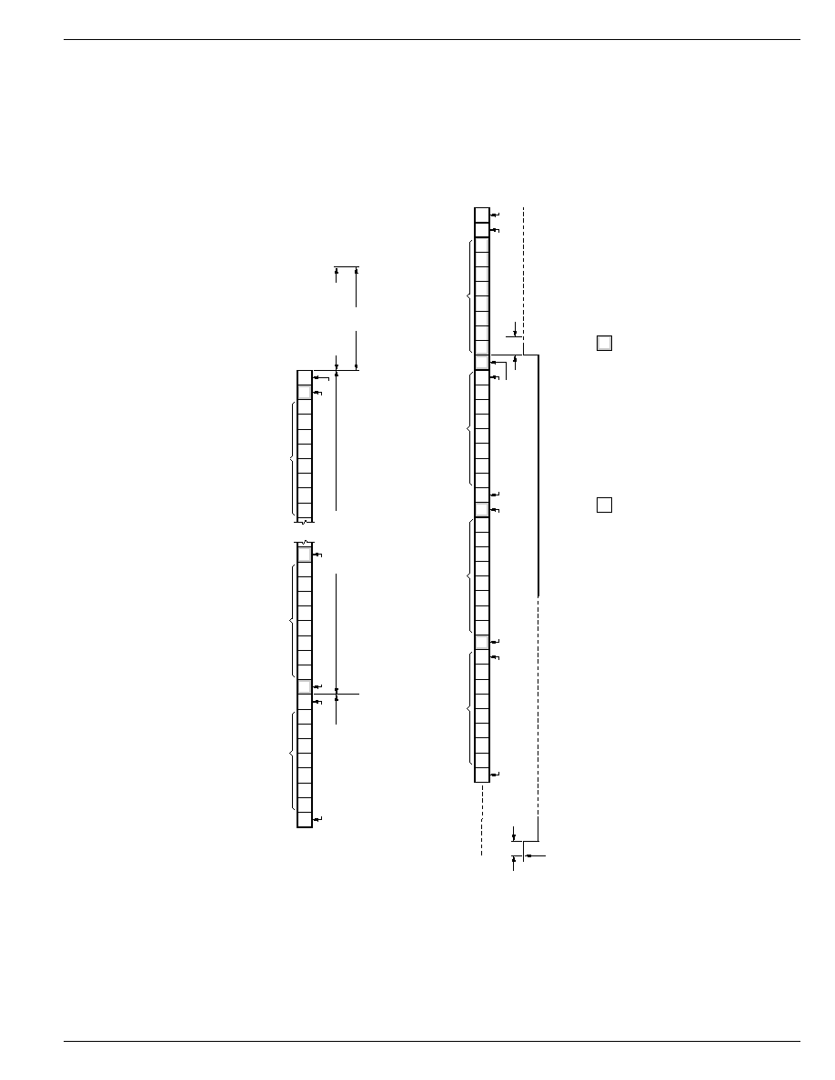
A/D Con
v
e
r
ter
in Standb
y
Con
v
ersion
in Prog
ress
Ne
w Con
v
ersion
in Prog
ress
Ne
w Con
v
ersion
Begins
Con
v
ersion Interr
upted
By MIC184 Ac
kno
wledge
Result
Ready
t
CONV
ST
OP
NO
T A
CKNO
WLEDGE
...
Figure 6.
A/D Converter Timing
A
SS
1000
A2
A1
A0
A2
A1
A0
0
A
00000001
A
1
0
1
00
X
X
XXXXXX
/
A
P
MIC184 Sla
v
e
Address
TEMP e
xceeds
T_SET or f
alls belo
w
T_HYST
MIC184 Sla
v
e
Address
D
ATA
INT*
Command Byte = 01
h
= CONFIG
CONFIG V
alue**
ST
AR
T
ST
AR
T
ST
OP
R/W =
WRITE
A
CKNO
WLEDGE
A
CKNO
WLEDGE
A
CKNO
WLEDGE
R/W = READ
NO
T A
CKNO
WLEDGE
Master-to-sla
v
e
tr
ansmission
Sla
v
e-to-master response
t
n/INT
t
/INT
*
Assumes INT P
olar
ity is activ
e lo
w
.
**
Status bits in CONFIG are cleared to z
ero f
ollo
wing this oper
ation.
Figure 7.
Responding to Interrupts

MIC184
Micrel
MIC184
10
November 2000
to be read from the MIC184 may then be clocked out. There
is one exception to this rule: If the location latched in the
pointer register from the last write operation is known to be
correct (i.e., points to the desired register), then the
"RECEIVE_DATA" procedure may be used. To perform a
RECEIVE_DATA, the host sends an address byte to select
the slave MIC184, and then retrieves the appropriate number
(one or two) of data bytes. Figures 1 through 5 show the
formats for these data read and data write procedures.
The command byte is 8 bits (1 byte) wide. This byte carries
the address of the MIC184 register to be operated upon, and
is stored in the MIC184's pointer register. The pointer register
is a write-only register, which is implemented for backward
compatibility to the National Semiconductor LM75 and similar
devices. The command byte (pointer register) values corre-
sponding to the various MIC184 register addresses are
shown in Table 2. Command byte values other than
0000 00XX
b
= 00
h
through 03
h
are reserved, and should not
be used.
The CONFIG register is 8 bits (1 byte) wide. Therefore,
communications with the CONFIG register will at a minimum
require a READ_BYTE, WRITE_BYTE, or a RECEIVE_BYTE.
The TEMP, T_HYST, and T_SET registers are logically nine
bits wide. Note, though, that these registers are physically
two bytes (one SMBus word) wide within the MIC184. Prop-
erly communicating with the MIC184 involves a 16-bit
READ_WORD or RECEIVE_WORD from, or WRITE_WORD
to, these registers. This is a requirement of the I
2
C/SMBus
serial data protocols, which only allow data transfers to occur
in multiples of eight bits.
Temperature Data Format
The LSB of each 9-bit logical register represents 0.5
∞
C. The
values are in a two's complement format, wherein the most
significant bit (D8) represents the sign: "0" for positive tem-
peratures and "1" for negative temperatures. The seven least
significant bits of each 16-bit physical register are undefined.
Therefore, physical bits D6 through D0 of the data read from
these registers must be masked off, and the resulting binary
value right justified before using the data received. It is also
possible to read only the first byte of any of these three
registers, sacrificing 0.5
∞
C of resolution in exchange for
somewhat simpler data handling. However, all writes to the
T_SET and T_HYST registers must be in the 16-bit
WRITE_WORD format. Table 3 shows examples of the data
format used by the MIC184 for temperatures.
A/D Converter Timing
Whenever the MIC184 is not in its low power shutdown mode,
the internal A/D converter (ADC) attempts to make continu-
ous conversions unless interrupted by a bus transaction
accessing the MIC184. When the MIC184 is accessed, the
conversion in progress will be halted, and the partial result
discarded. When the access of the MIC184 is complete the
ADC will begin a new conversion cycle, with results valid
t
CONV
after that. Figure 6 shows this behavior. t
CONV
is twice
as long for external conversions as it is for internal conver-
sions. This allows the use of a filter capacitor on the A2/T1
input without a loss of accuracy due to the resulting longer
settling times.
Power-On
When power is initially applied, the MIC184's internal regis-
ters are set to default states which make the MIC184 com-
pletely backward compatible with the LM75. Also at this time,
the levels on the address inputs A2, A1, and A0 are read to
establish the device's slave address. The MIC184's power-
up default state can be summarized as follows:
∑ Normal-mode operation
(MIC184 not in shutdown)
∑ ZONE is set to internal
(on-chip temperature sensing)
∑ INT function is set to comparator mode
∑ INT output is set to active-low operation
∑ Fault_Queue depth = 1
∑ Interrupts are enabled (IM = 0)
∑ T_SET = +80
∞
C; T_HYST = +75
∞
C
In order to accommodate the use of A2/T1 as a dual-purpose
input, there is a weak pulldown on A2/T1 that will attempt to
sink
25
µ
A from the pin to ground for t
POR
following power-
up of the MIC184. This allows the MIC184 to pull A2/T1 to a
low state when a diode junction is connected from that pin to
ground, and latch a zero as the A2 address value. If A2 is not
to be used as a diode connection, it should be connected to
V
DD
or ground. Note that a fault in the external temperature
sensor (if used) may not be reported until one or more
conversion cycles have been completed following power-on.
See DIODE FAULTS.
e
r
u
t
a
r
e
p
m
e
T
y
r
a
n
i
B
w
a
R
y
r
a
n
i
B
d
e
k
s
a
M
x
e
H
d
e
k
s
a
M
C
∞
5
2
1
+
X
X
X
X
X
X
X
0
1
0
1
1
1
1
1
0
0
1
0
1
1
1
1
1
0
b
A
F
0
h
C
∞
5
2
+
X
X
X
X
X
X
X
0
1
0
0
1
1
0
0
0
0
1
0
0
1
1
0
0
0
b
2
3
0
h
C
∞
5
.
0
+
X
X
X
X
X
X
X
1
0
0
0
0
0
0
0
0
1
0
0
0
0
0
0
0
0
b
1
0
0
h
C
∞
0
X
X
X
X
X
X
X
0
0
0
0
0
0
0
0
0
0
0
0
0
0
0
0
0
0
b
0
0
0
h
C
∞
5
.
0
≠
X
X
X
X
X
X
X
1
1
1
1
1
1
1
1
1
1
1
1
1
1
1
1
1
1
b
F
F
1
h
C
∞
5
2
≠
X
X
X
X
X
X
X
0
1
1
1
0
0
1
1
1
0
1
1
1
0
0
1
1
1
b
E
C
1
h
C
∞
0
4
≠
X
X
X
X
X
X
X
0
0
0
0
1
1
0
1
1
0
0
0
0
1
1
0
1
1
b
0
B
1
h
C
∞
5
5
≠
X
X
X
X
X
X
X
0
1
0
0
1
0
0
1
1
0
1
0
0
1
0
0
1
1
b
2
9
1
h
Table 3. Digital Temperature Format

November 2000
11
MIC184
MIC184
Micrel
Shutdown Mode
Setting the SHDN bit in the configuration register halts the
otherwise continuous conversions by the A/D converter. The
MIC184's power consumption drops to 1
µ
A typical in shut-
down mode. All registers may be read from, or written to,
while in shutdown mode. Serial bus activity will slightly
increase the MIC184's power consumption.
Entering shutdown mode will not affect the state of INT when
the device is in comparator mode (MODE = 0). However, If
the device is shut down while in interrupt mode, the INT pin
will be deasserted and the internal latch (STS) holding the
interrupt status will be cleared. Therefore, no interrupts will be
generated while the MIC184 is in shutdown mode, and the
interrupt status will not be retained. It is important to note,
however, that the
cause of the last temperature event will be
retained in the MIC184. This is described further in "Com-
parator and Interrupt Modes" below. The diode fault detection
mechanism (see "Diode Faults") requires one or more A/D
conversion cycles to detect external sensor faults. Hence, no
diode faults will be detected while the device is in shutdown.
Comparator and Interrupt Modes
Depending on the setting of the MODE bit in the configuration
register, the INT output will behave either as an interrupt
request signal or a thermostatic control signal. Thermostatic
operation is known as
comparator mode. The INT output is
asserted whenever the measured temperature, as reported
in the TEMP register, exceeds the threshold programmed in
the T_SET register for the number of conversions specified
by Fault_Queue (described below). In comparator mode, INT
will remain asserted unless and until the measured tempera-
ture falls below the value in the T_HYST register for
Fault_Queue conversions. No action on the part of the host
is required for operation in comparator mode. Note that
entering shutdown mode will not affect the state of INT when
the device is in comparator mode.
In
interrupt mode, once a temperature event has caused STS
to be set, and the INT output to be asserted, they will not be
automatically deasserted when the measured temperature
falls below T_HYST. They can only be deasserted by reading
any of the MIC184's internal registers or by putting the device
into SHUTDOWN mode. If the most recent temperature
event was an overtemperature condition, STS will not be set
again, and INT cannot be reasserted, until the device has
detected that TEMP < T_HYST. Similarly, if the most recent
temperature event was an undertemperature condition, STS
will in be set again, and INT cannot be reasserted, until the
device has detected that TEMP > T_SET. This keeps the
internal logic of the MIC184 backward compatible with that of
the LM75 and similar devices.
There is a software override for
this: while the MIC184 is operating in interrupt mode, the part
can be unconditionally set to monitor for an overtemperature
condition, regardless of what caused the last temperature
event. This is done by clearing the MODE bit, and then
immediately resetting it to 1. Following this sequence the next
temperature event detected will be an overtemperature con-
dition, regardless of whether the last temperature event was
the result of an overtemperature or undertemperature condi-
tion.
In both modes, the MIC184 will be responsive to overtem-
perature events upon power up.
Fault_Queue
A Fault_Queue (programmable digital filter) is provided in the
MIC184 to prevent false tripping due to thermal or electrical
noise. Two bits, CONFIG[4:3], set the depth of Fault_Queue.
Fault_Queue then determines the number of consecutive
temperature events (TEMP > T_SET or TEMP < T_HYST)
which must occur in order for the condition to be considered
valid. As an example, assume the MIC184 is in comparator
mode, and CONFIG[4:3] is programmed with 10
b
. Then the
measured temperature would have to exceed T_SET for four
consecutive A/D conversions before INT would be asserted
or the status bit set. Similarly, TEMP would have to be less
than T_HYST for four consecutive conversions before INT
would be reset.
Like any filter, the Fault_Queue function also has the effect of
delaying the detection of temperature events. In this ex-
ample, it would take 4
◊
t
CONV
to detect a temperature event.
The depth of Fault_Queue vs. D[4:3] of the configuration
register is shown in Table 4.
Handling Interrupts
The MIC184 may be either polled by the host, or request the
host's attention via the INT pin. In the case of polled opera-
tion, the host periodically reads the contents of CONFIG to
check the state of the status bit. The act of reading CONFIG
clears the status bit, STS. If more than one event that sets the
status bit occurs before the host polls the MIC184, only the
fact that at least one such event has occurred will be apparent
to the host.
If TEMP < T_HYST or TEMP > T_SET for Fault_Queue
conversions, the status bit STS will be set in the CONFIG
register. This action cannot be masked. However, a tempera-
ture event will only generate an interrupt signal on INT if
interrupts from the MIC184 are enabled (IM = 0 and MODE = 1
in the configuration register). Reading any register following
an interrupt will cause INT to be deasserted, and will clear
STS. The host should read the contents of the configuration
register after receiving an interrupt to confirm that the MIC184
was the source of the interrupt. This is shown in Figure 7. As
noted above, putting the device into shutdown mode will also
deassert INT and clear STS. Therefore, this usually should
not be done before completing the appropriate interrupt
service routine(s).
Since temperature-to-digital conversions continue while INT
is asserted, it is possible that temperature could change
between the MIC184's assertion of its INT output and the
host's response to the interrupt. It is good practice when
]
3
:
4
[
G
I
F
N
O
C
h
t
p
e
D
e
u
e
u
Q
_
t
l
u
a
F
0
0
*
n
o
i
s
r
e
v
n
o
c
1
1
0
s
n
o
i
s
r
e
v
n
o
c
2
0
1
s
n
o
i
s
r
e
v
n
o
c
4
1
1
s
n
o
i
s
r
e
v
n
o
c
6
g
n
i
t
t
e
s
t
l
u
a
f
e
D
*
Table 4. Fault_Queue Depth Settings

MIC184
Micrel
MIC184
12
November 2000
servicing interrupts for the host to read the current tempera-
ture to confirm that the condition that caused the interrupt still
exists.
Interrupt Polarity Selection
The INT output can be programmed to behave as an active-
low signal or an active-high signal. The default is active-low.
INT polarity is selected by programming the appropriate
value into the polarity bit (POL) in the CONFIG register.
Clearing POL selects active-low interrupts; setting POL se-
lects active-high interrupts. INT is an open-drain digital output
and may be wire-ORed with other open-drain logic signals.
Most applications will require a pull-up resistor on this pin.
Whether the CONFIG register's POL bit is set to provide a
current-sinking (low) or high-Z (high) state at the INT pin
when STS is high, writing a one to IM will put the INT pin into
a high-Z state. This meets the requirement of an active-low
interrupt for the SMBus, while making IM available as an INT-
forcing bit for those applications which employ an active-high
INT output (for example, software fan-control routines).
LM75 Compatibility
The MIC184 can be used interchangeably with the LM75 in
existing applications. The MIC184 offers several advantages
over the LM75:
∑ Ability to monitor a second, remote temperature
∑ Interrupt masking capability
∑ Status bit for software polling routines
∑ Lower quiescent current
∑ Supports single-byte reads from 16-bit registers
∑ No "inadvertent 8-bit read" bus lock-up issues
The three MSB's of the configuration register (which power
up as zeroes) are used to access the MIC184's additional
functions. These are reserved bits according to the LM75
specification and, for the LM75, must always be written as
zeroes. The MSB of the MIC184's status register is a status
flag that does not exist in the LM75. This bit will be set to one
whenever an overtemperature event occurs. This bit would
never be set by an LM75. Software should not depend on this
bit being zero when using the MIC184 as an LM75 upgrade.
If at power-up the measured temperature is higher than
T_SET, the status bit will be set following the first conversion
by the A/D. See "Applications Information" for a method by
which host software can use this fact to differentiate between
an MIC184 and an LM75.
November 2000
13
MIC184
MIC184
Micrel
Register Set and Programmer's Model
Internal Register Set
e
m
a
N
n
o
i
t
p
i
r
c
s
e
D
e
t
y
B
d
n
a
m
m
o
C
n
o
i
t
a
r
e
p
O
t
l
u
a
f
e
D
p
U
-
r
e
w
o
P
P
M
E
T
e
r
u
t
a
r
e
p
m
e
t
d
e
r
u
s
a
e
m
0
0
h
y
l
n
o
d
a
e
r
t
i
b
-
9
0
0
0
0
0
0
0
0
0
b
C
∞
0
)
1
(
G
I
F
N
O
C
r
e
t
s
i
g
e
r
n
o
i
t
a
r
u
g
i
f
n
o
c
1
0
h
e
t
i
r
w
/
d
a
e
r
t
i
b
-
8
0
0
0
0
0
0
0
0
b
)
2
(
T
S
Y
H
_
T
s
i
s
e
r
e
t
s
y
h
2
0
h
e
t
i
r
w
/
d
a
e
r
t
i
b
-
9
0
1
1
0
1
0
0
1
0
b
C
∞
5
7
+
T
E
S
_
T
t
n
i
o
p
t
e
s
e
r
u
t
a
r
e
p
m
e
t
3
0
h
e
t
i
r
w
/
d
a
e
r
t
i
b
-
9
0
0
0
0
0
1
0
1
0
b
C
∞
0
8
+
Detailed Register Descriptions
)
e
t
i
r
W
/
d
a
e
R
t
i
B
-
8
(
G
I
F
N
O
C
]
7
[
D
]
6
[
D
]
5
[
D
]
4
[
D
]
3
[
D
]
2
[
D
]
1
[
D
]
0
[
D
y
l
n
o
d
a
e
r
e
t
i
r
w
/
d
a
e
r
e
t
i
r
w
/
d
a
e
r
e
t
i
r
w
/
d
a
e
r
e
t
i
r
w
/
d
a
e
r
e
t
i
r
w
/
d
a
e
r
e
t
i
r
w
/
d
a
e
r
t
p
u
r
r
e
t
n
i
s
u
t
a
t
s
)
S
T
S
(
t
p
u
r
r
e
t
n
i
k
s
a
m
)
3
(
)
M
I
(
p
m
e
t
t
c
e
l
e
s
)
E
N
O
Z
(
e
u
e
u
q
t
l
u
a
f
h
t
p
e
d
)
Q
_
F
(
t
n
i
y
t
i
r
a
l
o
p
)
L
O
P
(
T
N
I
/
P
M
C
e
d
o
m
)
E
D
O
M
(
n
w
o
d
t
u
h
S
)
N
D
H
S
(
s
t
i
B
n
o
i
t
c
n
u
F
n
o
i
t
a
r
e
p
O
S
T
S
)
y
l
n
o
d
a
e
r
(
s
u
t
a
t
s
t
p
u
r
r
e
t
n
i
e
n
o
n
=
0
,
d
e
r
u
c
c
o
t
p
u
r
r
e
t
n
i
=
1
M
I
k
s
a
m
t
p
u
r
r
e
t
n
i
d
e
l
b
a
s
i
d
=
1
,
d
e
l
b
a
n
e
=
0
E
N
O
Z
n
o
i
t
c
e
l
e
s
e
r
u
t
a
r
e
p
m
e
t
e
t
o
m
e
r
/
l
a
n
r
e
t
n
i
l
a
n
r
e
t
n
i
=
0
,
e
t
o
m
e
r
=
1
Q
_
F
h
t
p
e
d
e
u
e
u
Q
_
t
l
u
a
F
,
s
n
o
i
s
r
e
v
n
o
c
2
=
1
0
,
n
o
i
s
r
e
v
n
o
c
1
=
0
0
s
n
o
i
s
r
e
v
n
o
c
6
=
1
1
,
s
n
o
i
s
r
e
v
n
o
c
4
=
0
1
L
O
P
n
o
i
t
c
e
l
e
s
y
t
i
r
a
l
o
p
t
u
p
t
u
o
T
N
I
w
o
l
e
v
i
t
c
a
=
0
,
h
g
i
h
e
v
i
t
c
a
=
1
E
D
O
M
t
p
u
r
r
e
t
n
i
/
r
o
t
a
r
a
p
m
o
c
n
i
p
T
N
I
r
o
f
n
o
i
t
c
e
l
e
s
e
d
o
m
,
e
d
o
m
t
p
u
r
r
e
t
n
i
=
1
e
d
o
m
r
o
t
a
r
a
p
m
o
c
=
0
N
D
H
S
n
w
o
d
t
u
h
s
/
l
a
m
r
o
n
n
o
i
t
c
e
l
e
s
e
d
o
m
g
n
i
t
a
r
e
p
o
,
n
w
o
d
t
u
h
s
=
1
l
a
m
r
o
n
=
0
Power-Up Default Value: 0000 0000
b
= 00
h
(4)
∑ not in shutdown mode
∑ comparator mode
∑ INT = active low
∑ Fault_Queue depth = 1
∑ local temperature zone
∑ interrupts enabled.
CONFIG Command Byte Address: 0000 0001
b
= 01
h
(1)
TEMP will contain measured temperature data for the selected
zone after the completion of one conversion.
(2)
After the first Fault_Queue conversions are complete, the
status bit will be set if TEMP < T_HYST or TEMP > T_SET.
(3)
Setting IM forces the open-drain INT output into its high-Z
state. See "INT Polarity Selection."
(4)
After the first Fault_Queue conversions are completed, the
status bit will be set if TEMP < T_HYST or TEMP > T_SET.
MIC184
Micrel
MIC184
14
November 2000
T_SET Power-Up Default Value: 0 1010 0000b (+80
∞
C)
T_SET Command Byte Address: 0000 0011b = 03
h
* The value in T_SET is 9 logical bits in width, but due to the
conventions of I
2
C/SMBus, it is represented by 16 serial bits.
System software should ignore undefined bits D[6:0] during
register reads. Bits [6:0] should be set to zero during register
writes. See Serial Port Operation" and "Temperature Data
Format" for more details.
Temperature Setpoint Register
)
e
t
i
r
W
/
d
a
e
R
t
i
B
-
9
(
T
E
S
_
T
]
5
1
[
D
]
4
1
[
D
]
3
1
[
D
]
2
1
[
D
]
1
1
[
D
]
0
1
[
D
]
9
[
D
]
8
[
D
]
7
[
D
]
6
[
D
]
5
[
D
]
4
[
D
]
3
[
D
]
2
[
D
]
1
[
D
]
0
[
D
B
S
M
7
t
i
b
6
t
i
b
5
t
i
b
4
t
i
b
3
t
i
b
2
t
i
b
1
t
i
b
B
S
L
X
X
X
X
X
X
X
t
n
i
o
p
t
e
s
e
r
u
t
a
r
e
p
m
e
t
r
e
v
o
s
t
i
B
n
o
i
t
c
n
u
F
n
o
i
t
a
r
e
p
O
]
7
:
5
1
[
D
t
n
i
o
p
t
e
s
r
o
t
a
r
a
p
m
o
c
e
r
u
t
a
r
e
p
m
e
t
r
e
v
o
*
e
t
i
r
w
/
d
a
e
r
T_HYST Power-Up Default Value: 0 1001 0110
b
(+75
∞
C)
T_HYST Command Byte Address: 0000 0010b = 02
h
* The value in T_HYST is 9 logical bits in width, but due to the
conventions of I
2
C/SMBus, it is represented by 16 serial bits.
System software should ignore undefined bits D[6:0] during
register reads. Bits [6:0] should be set to zero during register
writes. See "Serial Port Operation" and "Temperature Data
Format" for more details.
Hysteresis Register
)
e
t
i
r
W
/
d
a
e
R
t
i
B
-
9
(
T
S
Y
H
_
T
]
5
1
[
D
]
4
1
[
D
]
3
1
[
D
]
2
1
[
D
]
1
1
[
D
]
0
1
[
D
]
9
[
D
]
8
[
D
]
7
[
D
]
6
[
D
]
5
[
D
]
4
[
D
]
3
[
D
]
2
[
D
]
1
[
D
]
0
[
D
B
S
M
7
t
i
b
6
t
i
b
5
t
i
b
4
t
i
b
3
t
i
b
2
t
i
b
1
t
i
b
B
S
L
X
X
X
X
X
X
X
g
n
i
t
t
e
s
s
i
s
e
r
e
t
s
y
h
e
r
u
t
a
r
e
p
m
e
t
s
t
i
B
n
o
i
t
c
n
u
F
n
o
i
t
a
r
e
p
O
]
7
:
5
1
[
D
g
n
i
t
t
e
s
s
i
s
e
r
e
t
s
y
h
e
r
u
t
a
r
e
p
m
e
t
*
e
t
i
r
w
/
d
a
e
r
Temperature Result Register
)
y
l
n
O
d
a
e
R
t
i
B
-
9
(
P
M
E
T
]
5
1
[
D
]
4
1
[
D
]
3
1
[
D
]
2
1
[
D
]
1
1
[
D
]
0
1
[
D
]
9
[
D
]
8
[
D
]
7
[
D
]
6
[
D
]
5
[
D
]
4
[
D
]
3
[
D
]
2
[
D
]
1
[
D
]
0
[
D
B
S
M
7
t
i
b
6
t
i
b
5
t
i
b
4
t
i
b
3
t
i
b
2
t
i
b
1
t
i
b
B
S
L
X
X
X
X
X
X
X
C
D
A
m
o
r
f
a
t
a
d
e
r
u
t
a
r
e
p
m
e
t
s
t
i
B
n
o
i
t
c
n
u
F
n
o
i
t
a
r
e
p
O
]
7
:
5
1
[
D
a
t
a
d
e
r
u
t
a
r
e
p
m
e
t
d
e
r
u
s
a
e
m
e
n
o
z
d
e
t
c
e
l
e
s
r
o
f
*
y
l
n
o
d
a
e
r
Power-Up Default Value: 0 0000 0000
b
= 0
∞
C
TEMP Command Byte Address: 0000 0000
b
= 00
h
* The value in TEMP is 9 logical bits in width, but due to the
conventions of I
2
C/SMBus, it is represented by 16 serial bits.
System software should ignore undefined bits D[6:0]. See
"Serial Port Operation" and "Temperature Data Format" for
more details.
TEMP will contain measured temperature data for the selected
zone after the completion of one conversion.

November 2000
15
MIC184
MIC184
Micrel
Applications Information
Switching Zones
The recommended procedure for switching between the
internal and external zones is as follows:
1. Disable interrupts (if used)
by setting the IM bit in CONFIG.
2. Read the CONFIG register to:
a) Verify no masked interrupt was pending
(D[7] = 0)
b) Clear STS prior to switching zones
c) Hold the settings of CONFIG register for the
current zone
3. Write the appropriate values to
T_SET and T_HYST for the new zone.
4. Write to CONFIG as follows:
a) To toggle the ZONE bit (1 = remote, 0 =
internal)
b) If interrupts are being used, step 4 should
also clear MODE
5. If interrupts are being used, MODE must then be
set to 1 and IM reset to 0
At the conclusion of the serial bus transaction for step 4, the
A/D converter will begin a conversion cycle using the new
zone setting. The next conversion cycle completed
after the
serial bus transaction for step 5 will result in the state of the
INT output being updated (if enabled) for the new zone.
Generally the MIC184's A/D converter operates continu-
ously, but it will be halted and reset each time the part
recognizes its slave address on the serial bus. Interrupted
conversions will remain halted until the end of the host's
communication with the MIC184. After the completion of step
5 and a delay of
t
CONV
x Fault_Queue, STS and INT will
contain the results for the new zone. The above routine is
extremely unlikely to miss a temperature event, as even one
A/D conversion is typically much slower than the I
2
C/SMBus
transactions that control the MIC184. See Figure 6: A/D
Converter Timing.
Step 2(c) is recommended because the MIC184 has only one
CONFIG register, corresponding to the active zone. In order
to preserve data integrity for both zones, 2(c) allows the host
to create a virtual CONFIG register for the inactive zone by
dedicating one byte of memory to that purpose. Additional
virtual registers may be created as needed by inserting
additional reads as steps 2(d), 2(e), etc. These could for
example correspond to the values in T_SET and T_HYST
immediately prior to switching zones. Steps 4(b) and 5
ensure that the MIC184 will enter the new zone searching for
an overtemperature event.
Identifying an MIC184 by Software Test
The MIC184 and the LM75 each have an eight-bit
CONFIG register. In LM75-type parts, no more than seven
of the eight bits of this register are used, and at least one
bit (the MSB) will always return a zero. The MIC184 uses
all eight bits of the CONFIG register: the MSB is the part's
status bit (STS). A simple test by which the host can
determine whether a system has an MIC184 installed, or is
using a legacy LM75-type device, is to create a situation
which will set the MSB in the MIC184's CONFIG register
and then determine if the MSB is in fact set. Two examples
of how this can be done are outlined below. The first is
interrupt-driven, the second uses software polling. Note
that both procedures generate one or more spurious
interrupts. The code for these tests should therefore
temporarily disable any affected interrupt routines.
{START Interrupt-Driven Test and Initialization
Routine}
1. Disable the host's overtemperature and
undertemperature interrupt handling routine.
Redirect interrupts from the part under test to a
handler for the interrupt that will be generated in
steps (4) and (7) of this routine.
2. Write 0000 0010b (02h) to the CONFIG register.
(The assumption is made that the host is an I
2
C
or SMBus part, and therefore responds to an
active-low interrupt request.)
3. Write 1100 1000 1000 0000b = C880h to T_SET
and T_HYST. This corresponds to -55.5
∞
C.
4. When the part has finished its first A/D conver-
sion, INT will be asserted.
5. Read out the contents of the CONFIG register:
a) If the part is an MIC184, the MSB will be set
to one (CONFIG = 1000 0010b = 82h).
b) If the part is a conventional LM75-type part,
the MSB will be zero (CONFIG = 0000
0010b = 02h).
6.Write 0111 1111 1000 0000b = 7F80h to T_SET
and T_HYST. This corresponds to +127.5
∞
C.
7.When the part has finished its next A/D conver-
sion, INT will be asserted a second time.
8.Read CONFIG again, to clear the interrupt
request from step (7). This will also clear STS, if
the part under test is an MIC184.
9.Based on the results of the test in step (4), do the
following within 50ms total:
a) Set the CONFIG register as required.
b) Load T_HYST with its operational value.
c)
Load T_SET with its operational value.
d) Set the host's interrupt handling routine back
to overtemperature and undertemperature
mode.
{END}

MIC184
Micrel
MIC184
16
November 2000
{START Polling-Based Test and Initialization
Routine}
1. Temporarily disable the host's interrupt input
from the device under test.
2. Write 0000 0010b (02h) to the CONFIG register.
3. Write 1100 1000 1000 0000b = C880h to T_SET
and T_HYST. This corresponds to -55.5
∞
C.
4. Wait t
conv
(160ms max.) for the part to finish at
least one A/D conversion.
5. Read the contents of the CONFIG register:
a) If the part is an MIC184, the MSB will be set
to one (CONFIG = 82h).
b) If the part is a conventional LM75-type part,
the MSB will be zero (CONFIG = 02h).
6. Write 0111 1111 1000 0000b = 7F80h to T_SET
and T_HYST. This corresponds to +127.5
∞
C.
7. Wait an additional t
conv
for the part to finish a
second conversion.
8. Read CONFIG again, to clear the interrupt
request from step (7). This will also clear STS, if
the part under test is an MIC184.
9. Based on the results of the test in step (4), do
the following four steps within 50ms total:
a) Set the CONFIG register as required.
b) Load T_HYST with its operational value.
c)
Load T_SET with its operational value.
d) Re-enable the host's interrupt handling input
from the part under test.
{END}
These routines force the device under test to generate an
overtemperature fault (steps 3 and 4), followed by an
undertemperature fault (steps 6 through 8). This sequence
causes the device under test to exit the routine prepared to
respond to an overtemperature condition. If being immedi-
ately prepared to detect an undertemperature condition upon
exit is desired, swap steps 3 and 6 in each routine.
Remote Diode Selection
Most small-signal PNP transistors with characteristics similar
to the JEDEC 2N3906 will perform well as remote tempera-
ture sensors. Table 3 lists several examples of such parts.
Micrel has tested those marked with a bullet for use with the
MIC184.
Vendor
Part Number
Package
Tested
Fairchild
MMBT3906
SOT-23
On Semiconductor
MMBT3906L
SOT-23
Phillips Semiconductor
PMBT3906
SOT-23
Rohm Semiconductor
SST3906
SOT-23
Samsung
KST3906-TF
SOT-23
Zetex
FMMT3906
SOT-23
Table 5. Transistors Suitable for Remote Temperature Sensing Use
Minimizing Errors
Self-Heating
One concern when using a part with the temperature accu-
racy and resolution of the MIC184 is to avoid errors induced
by self-heating (V
DD
◊
I
DD
). In order to understand what level
of error this might represent, and how to reduce that error, the
dissipation in the MIC184 must be calculated, and its effects
examined as a temperature error.
In most applications, the INT output will be low for at most a
few milliseconds before the host sets it back to the high state,
making its duty cycle low enough that its contribution to self-
heating of the MIC184 is negligible. Similarly, the DATA pin
will in all likelihood have a duty cycle of substantially below
25% in the low state. These considerations, combined with
more typical device and application parameters, allow the
following calculation of typical device self-heating in interrupt-
mode:
P
D
= (I
DD(typ.)
3.3V + 25% I
OL(data)
0.3V +
1% I
OL(int)
0.3V)
P
D
= (0.3mA
◊
3.3V + 25%
◊
1.5mA
◊
0.3V +
1%
◊
1.5mA
◊
0.3V)
T
J
= 1.11mW
◊
206
∞
C/W
T
J
relative to T
A
is 0.23
∞
C
If the part is to be used in comparator mode, calculations
similar to those shown above (accounting for the expected
value and duty cycle of I
OL(int)
) will give a good estimate of the
device's self-heating error.
In any application, the best test is to verify performance
against calculation in the final application environment. This
is especially true when dealing with systems for which some
of the thermal data, (for example, PC board thermal conduc-
tivity and/or ambient temperature), may be poorly defined or
unavailable except by empirical means.
Series Resistance
The operation of the MIC184 depends upon sensing the
V
CB-E
of a diode-connected PNP transistor ("diode") at two
different current levels. For remote temperature measure-
ments, this is done using an external diode connected be-
tween A2/T1 and ground.
Since this technique relies upon measuring the relatively
small voltage difference resulting from two levels of current
through the external diode, any resistance in series with the
external diode will cause an error in the temperature reading

November 2000
17
MIC184
MIC184
Micrel
from the MIC184. A good rule of thumb is this: for each ohm
in series with the external transistor, there will be a 0.9
∞
C error
in the MIC184's temperature measurement. It is not difficult
to keep the series resistance well below an ohm (typically
0.1
), so in most systems this will not be an issue.
Filter Capacitor Selection
When using a remote diode for temperature sensing, it is
sometimes desirable to use a filter capacitor between the A2/
T1 and GND pins of the MIC184. The use of this capacitor is
recommended in environments with a significant high fre-
quency noise (such as digital switching noise), or if long wires
are used to connect to the remote diode. The maximum
recommended total capacitance from the A2/T1 pin to GND
is 2700pF. This usually suggests the use of a 2200pF NP0 or
C0G ceramic capacitor with a 10% tolerance.
If the remote diode is to be at a distance of more than 6" ~ 12"
from the MIC184, using a shielded cable (solid foil shield
microphone cable is a good choice) for the connections to the
diode can significantly help reduce noise pickup. Remember
to subtract the cable's conductor-to-shield capacitance from
the 2700pF maximum total capacitance.
Layout Considerations
Local Mode Only Applications:
If the MIC184 is not going to be used with an external diode,
the best layout is one which keeps it thermally coupled to the
subsystem(s) whose temperature it must monitor, while
avoiding any strong sources of EMI, RFI, or electrostatically
coupled noise. Two of the most common examples of such
sources are switching power supply transformers and CRTs.
Remote Mode Applications:
1. If the remote sensing capability of the MIC184
will be used in an application, place the MIC184
as close to the remote diode as possible, while
taking care to avoid severe noise sources (high
frequency power transformers, CRTs, memory
and data busses, and the like).
2. Since any conductance from the various volt-
ages on the PC Board and the A2/T1 pin can
induce serious errors, it is good practice to
guard the remote diode's emitter trace with a
pair of ground traces. These ground traces
should be returned to the MIC184's own ground
pin. They should
not be grounded at any other
part of their run. However, it
is highly desirable
to use these guard traces to carry the diode's
own ground return back to the ground pin of the
MIC184, thereby providing a Kelvin connection
for the base of the diode. See Figure 8.
3. When using the MIC184 to sense the tempera-
ture of a processor or other device which has an
integral on-board "diode" (e.g., Intel's Pentium
Æ
III), connect the emitter and base of the remote
sensor to the MIC184 using the guard traces
and Kelvin return shown in Figure 8. The
collector of the remote "diode" is inaccessible to
the user on these types of chips. To allow for
this, the MIC184 has superb rejection of noise
appearing from collector to GND, as long as the
base to ground connection is relatively quiet.
4. Due to the small currents involved in the mea-
surement of the remote diode's
V
BE
, it is
important to adequately clean the PC board after
soldering. This is most likely to show up as an
issue in some situations where water-soluble
soldering fluxes are used.
5. In general, wider traces for the ground and A2/
T1 pins will help reduce susceptibility to radiated
noise (wider traces are less inductive). Use
trace widths and spacing of 10 mils wherever
possible. Wherever possible, place a ground
plane under the MIC184, and under the connec-
tions from the MIC184 to the remote diode. This
will help guard against stray noise pickup.
6. Always place a good quality V
DD
bypass capaci-
tor directly adjacent to, or underneath, the
MIC184. This part should be a 0.1
µ
F ceramic
capacitor. Surface-mount parts provide the best
bypassing because of their low inductance.
7. When the MIC184 is being powered from
particularly noisy power supplies, or from
supplies which may have sudden high-amplitude
spikes appearing on them, it can be helpful to
add additional power supply filtering. This
should be implemented as a 100
resistor in
series with the part's V
DD
pin, and a 4.7
µ
F, 6.3V
electrolytic capacitor from V
DD
to GND. See
Figure 9.
MIC184
Micrel
MIC184
18
November 2000
REMOTE DIODE (A2/T1)
GUARD/RETURN
1
2
3
DATA
CLK
INT
GND
8
7
6
5
4
VDD
A0
A1
A2/T1
GUARD/RETURN
Figure 8. Guard Traces/Kelvin Ground Returns
DATA
1
2
3
8
4
5
6
7
FROM
SERIAL BUS
HOST
2N3906
2200pF
MIC184
CLK
INT
VDD
100
3.0V to 3.6V
10k Pull-ups
A2/T1
A1
A0
GND
4.7
µ
F
0.1
µ
F
Figure 9. V
DD
Decoupling for Very Noisy Supplies
November 2000
19
MIC184
MIC184
Micrel
Package Information
45
∞
0
∞
≠8
∞
0.244 (6.20)
0.228 (5.79)
0.197 (5.0)
0.189 (4.8)
SEATING
PLANE
0.026 (0.65)
MAX
)
0.010 (0.25)
0.007 (0.18)
0.064 (1.63)
0.045 (1.14)
0.0098 (0.249)
0.0040 (0.102)
0.020 (0.51)
0.013 (0.33)
0.157 (3.99)
0.150 (3.81)
0.050 (1.27)
TYP
PIN 1
DIMENSIONS:
INCHES (MM)
0.050 (1.27)
0.016 (0.40)
8-Lead SOP (M)
0.008 (0.20)
0.004 (0.10)
0.039 (0.99)
0.035 (0.89)
0.021 (0.53)
0.012 (0.03) R
0.0256 (0.65) TYP
0.012 (0.30) R
5
∞
MAX
0
∞
MIN
0.122 (3.10)
0.112 (2.84)
0.120 (3.05)
0.116 (2.95)
0.012 (0.03)
0.007 (0.18)
0.005 (0.13)
0.043 (1.09)
0.038 (0.97)
0.036 (0.90)
0.032 (0.81)
DIMENSIONS:
INCH (MM)
0.199 (5.05)
0.187 (4.74)
8-Lead MSOP (MM)

MIC184
Micrel
MIC184
20
November 2000

November 2000
21
MIC184
MIC184
Micrel
MICREL INC.
1849 FORTUNE DRIVE
SAN JOSE, CA 95131
USA
TEL
+ 1 (408) 944-0800
FAX
+ 1 (408) 944-0970
WEB
http://www.micrel.com
This information is believed to be accurate and reliable, however no responsibility is assumed by Micrel for its use nor for any infringement of patents or
other rights of third parties resulting from its use. No license is granted by implication or otherwise under any patent or patent right of Micrel Inc.
© 2000 Micrel Incorporated