
September 2000
1
MIC2010/2070
MIC2010
Micrel
MIC2010/MIC2070
USB Power Controller
Advance Information
General Description
The MIC2010 is a dual channel USB power switch designed
to support the power distribution requirements for USB Wakeup
from the ACPI S3 state. The MIC2010 will directly switch its
two outputs between a 5V main supply and a 5V auxiliary
supply normally provided in ATX style power supplies.
The MIC2010 will adjust its current-limit threshold according
to the ACPI state it is in. In the normal active ACPI S0 state
the current-limit is set at 500mA minimum per channel
satisfying the USB continuous output current specification. In
the S3 state the current-limit can be reduced to a value
determined by an external resistor to minimize the current
that is supplied by the auxiliary supply, thereby ensuring that
voltage regulation is maintained even during fault conditions.
The MIC2010 provides make-before-break switching to en-
sure glitch-free transitions between the S3 and S0 states.
Each channel is also thermally isolated from the other so that
a fault in one channel does not effect the other. FAULT status
output signals are also provided indicating overcurrent and
thermal shutdown conditions.
The MIC2070 option latches the output off upon detecting an
overcurrent condition lasting for more than 5ms minimum.
The output can be reset by either toggling the EN inputs of the
MIC2070-1/-2 or by removing the load. Latching the output
off provides a circuit breaker mode of operation which re-
duces power consumption during fault conditions.
Typical Application
MIC2010-1P/-2P
V
BUS
D+
D�
GND
MAIN
AUX
OUT1
EN1
EN2
Downstream
USB
Port 1
100
�
F
5V MAIN
ATX Power Supply
S3#
FAULT1
FAULT1
V
BUS
D+
D�
GND
Downstream
USB
Port 2
OUT2
RSET1
RSET2
GND
5V STANDBY
82801AA or Equivalent
SLP S3#
SLP S5#
OC0
OC1
Overcurrent Port 1
Overcurrent Port 1
ON/OFF 1
ON/OFF 2
100
�
F
S3# CONTROL
Figure 1. USB Wakeup From ACPI S3 System Diagram
Features
� Compliant to USB power distribution specifications
� Two completely independent switches
� Integrated switching matrix supports ACPI S0/S3 state
transitions without external FET circuits
� Make-before-break switching ensures glitch-free
transitions
� No back-feed of auxiliary supply onto main supply
during standby mode
� Bi-level current-limit preserves auxiliary supply voltage
regulation in standby mode
� Thermally isolated channels
� Thermal shutdown protection
� Fault status outputs with filter prevents false assertions
during hot-plug events
� Circuit breaker options with auto-reset (MIC2070)
� Undervoltage lockout
Applications
� Desktop PCs
� Notebook PCs
� Notebook docking stations
� LAN Servers
� PC motherboard
Micrel, Inc. � 1849 Fortune Drive � San Jose, CA 95131 � USA � tel + 1 (408) 944-0800 � fax + 1 (408) 944-0970 � http://www.micrel.com
MIC2010
Micrel
MIC2010
2
September 2000
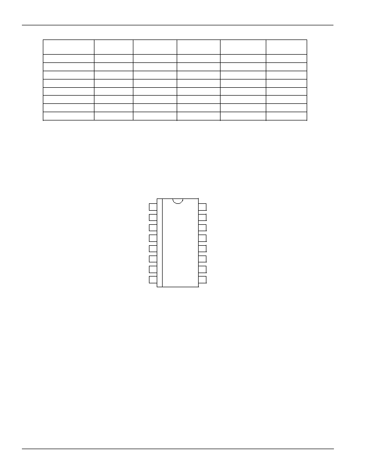
Pin Configuration
1
FAULT1
EN1
S3#
RSET1
AUX
NC
RSET2
GND
16 FAULT2
EN2
OUT1
OUT1
MAIN
MAIN
OUT2
OUT2
15
14
13
12
11
10
9
2
3
4
5
6
7
8
16-Pin QSOP (QS)
Ordering Information
Fault
Circuit Breaker
Temperature
Part Number
Enable
Output
Function
Range
Package
MIC2010-1CQS*
Active High
Open-Drain
0
�
C to +70
�
C
16-lead QSOP
MIC2010-1PCQS*
Active High
Internal Pull-Up
0
�
C to +70
�
C
16-lead QSOP
MIC2010-2CQS*
Active Low
Open-Drain
0
�
C to +70
�
C
16-lead QSOP
MIC2010-2PCQS
Active Low
Internal Pull-Up
0
�
C to +70
�
C
16-lead QSOP
MIC2070-1CQS
Active High
Open-Drain
0
�
C to +70
�
C
16-lead QSOP
MIC2070-1PCQS*
Active High
Internal Pull-Up
0
�
C to +70
�
C
16-lead QSOP
MIC2070-2CQS*
Active Low
Open-Drain
0
�
C to +70
�
C
16-lead QSOP
MIC2070-2PCQS*
Active Low
Internal Pull-Up
0
�
C to +70
�
C
16-lead QSOP
* Contact factory for availability.

September 2000
3
MIC2010/2070
MIC2010
Micrel
Pin Description
Pin Number
Pin Name
Pin Function
1
FAULT1
Fault Status (Output): Channel 1, active-low; weak pull-up to AUX or open-
drain. FAULT1 is asserted LOW when channel 1 is in a thermal shutdown
state or overcurrent condition for more than 5ms. MIC2070 latches this
output in its asserted state upon overcurrent condition. Toggling EN1 or
removing the load will reset the circuit breaker latch, and deassert FAULT1.
2
EN1
Enable (Input): Channel 1, active-high (�1) or active-low (�2). Toggling this
input also resets the latched output of the MIC2070.
3
S3#
Control (Input): When this input is high, the MAIN inputs are connected to
OUT1 and OUT2 via 100m
, 500mA MOSFET switches. When this input is
LOW, the AUX inputs are connected to OUT1 and OUT2 via 500m
MOSFET switches with a current-limit threshold specified by external
resistors, RSET1 and RSET2.
4
RSET1
Current-Limt Set Resistor (Input): Channel 1. A resistor connected to this
input sets the current-limit threshold in AUX mode (S3# asserted). The
current-limit threshold is determined by approximately 18/RSET1.
5
AUX
Auxiliary 5V Supply (Input): Also used as power supply for internal circuitry.
6
NC
No Connection: This pin may be connected to other pins without restriction.
7
RSET2
Current-Limit Set Resistor (Input): Channel 2. A resistor connected to this
input sets the current-limit threshold in AUX mode (S3# asserted). The
current-limit threshold is determined by approximately 18/RSET2.
8
GND
Ground
9, 10
OUT2
Channel 2 (Output): Both pins must be connected together externally.
11, 12
MAIN
5V Main Supply (Input): All MAIN inputs must be connected together
externally.
13, 14
OUT1
Channel 1 (Output): Both pins must be connected together externally.
15
EN2
Enable (Input): Channel 2, active-high (�1) or active-low (�2). Toggling this
input also resets the latched output for the MIC2070.
16
FAULT2
Fault Status (Output): Channel 2, active-low; weak pull-up to AUX or open-
drain. FAULT2 is asserted LOW when channel 2 is in a thermal shutdown
state or overcurrent condition for more than 5ms. MIC2070 latches this
output in it's asserted state upon overcurrent condition. Toggling EN2 or
removing load will reset the circuit breaker latch, and deassert FAULT2.

MIC2010
Micrel
MIC2010
4
September 2000
Absolute Maximum Ratings
(Note 1, Note 4)
Supply Voltage (V
IN
) ........................................ �0.3V to 6V
FAULT#, OUT1, OUT2 Output Pins ................. �0.3V to 6V
FAULT1,FAULT2, Output Current .............................. 25mA
ESD Rating, Note 3 ...................................................... 2kV
Operating Ratings
(Note 2)
Supply Voltage (V
MAIN,
V
AUX
) ..................... +4.5V to +5.5V
Continuous Output Current (AUX Mode) .. 50mA to 300mA
Ambient Temperature (T
A
) ........................... �0
�
C to +70
�
C
Junction Temperature (T
J
) ....................... Internally Limited
Package Thermal Resistance
QSOP
(
JA
) ........................................................ 163
�
C/W
Electrical Characteristics
V
MAIN
= 5V; AUX = 5V; R
SET
= 125
, T
A
= 25
�
C.
Symbol
Parameter
Condition
Min
Typ
Max
Units
V
MAIN
MAIN Supply Voltage
4.5
5.0
5.5
V
I
MAIN
MAIN Supply Current
S3# = 1, both switches ON, no load
16
22
�
A
Note 5
S3# = 1, both switches OFF, no load
5
�
A
I
LEAK
MAIN Reverse Leakage Current,
S3# = 0, both switches ON, V
MAIN
= 0V
�10
+10
�
A
Note 5
V
AUX
AUX Supply Voltage
4.5
5.0
5.5
V
I
AUX
AUX Supply Current, Note 5
S3# = 0; No load, both switches ON
.6
1
mA
S3# = 0; No load, both switches OFF
5
�
A
V
UV/AUX
AUX Undervoltage Lockout
V
AUX
increasing
3.5
3.7
4.0
V
Threshold
V
AUX
decreasing
3.3
3.5
3.8
V
V
HYS
AUX Undervoltage Lockout
200
mV
Hysteresis
R
DSMAIN
MAIN On-Resistance, Each Output
S3# = 1, I
OUT
= 500mA
100
140
m
R
DSAUX
AUX On-Resistance, Each Output
S3# = 0, I
OUT
= 100mA
500
700
m
I
LIMIT
MAIN Current-Limit Threshold,
S3# = 1, V
OUT
= 4.0V, ramped load
0.5
1.25
A
MAIN Short-Circuit Current-Limit
V
OUT
= 0V
0.5
1.25
A
Current-Limit Factor (AUX Supply),
S3# = 0, I
OUT
= 50mA to 300mA
14.4
18
21.6
A �
Note 6
V
OUT
= 4V
V
TH
S3#, EN1, EN2
High-to-Low transition
.8
1.5
V
Input Threshold Voltage
Low-to-High transition
1.7
2.0
V
I
IN
S3#, EN1, EN2 Input Current
V
S3/EN
=5V, 0V
�1
1
�
A
V
HYS
EN1, EN2 and S3# Input Hysteresis
200
mV
I
OFF
OUT1, 2 Leakage Current
Outputs are off, V
OUT
= 0
�10
10
�
A
Pull-Up Current During Latched
Outputs latched off
TBD
1
TBD
mA
Output State (MIC2070-x only)
V
TH LATCH
Latch Reset Threshold
V
OUT
rising
1.95
V
Minimum Output Slew Rate
Output rising
.4
V/s
to Reset Latch (MIC2070-x only),
Note 7
Overtemperature Threshold
T
J
increasing, single channel
140
�
C
T
J
decreasing, single channel
120
�
C
T
J
increasing, both channels
160
�
C
T
J
decreasing, both channels
150
�
C
V
OL
FAULT1, 2 Output Low Voltage
I
FAULT
= 5mA
0.2
V
FAULT1, 2 Output Off Current
V
FAULT
= 5V
0.2
10
�
A
(Not Applicable for 'P' versions)

September 2000
5
MIC2010/2070
MIC2010
Micrel
Symbol
Parameter
Condition
Min
Typ
Max
Units
V
OH
FAULT1, 2 Output High Voltage
I
FAULT
= �20
�
A
4
V
(MIC2010-1P, 2P), (MIC2070-1P, 2P)
T
H
MAIN to S3# Hold Time, Note 7
Figure 5
5
ms
T
S
MAIN to S3# Set-up Time, Note 7
Figure 5
0
ms
t
DLY
FAULT Delay Filter Response Time
Output shorted to ground, Figure 4
5
10
20
ms
(Overcurrent only), Note 8
t
OC
Overcurrent Response Time
Output shorted to ground, Figure 4
MAIN output
2
�
s
AUX output
2
�
s
t
ON(MAIN)
MAIN Output Turn-On Time
R
L
= 10
, C
L
= 1
�
F, Figure 3
2
ms
t
OFF(MAIN)
MAIN Output Turn-Off Time
R
L
= 10
, C
L
= 1
�
F, Figure 3
35
�
s
t
r(MAIN)
MAIN Output Rise Time
R
L
= 10
, C
L
= 1
�
F, Figure 3
2
ms
t
f(MAIN)
MAIN Output Fall Time
R
L
= 10
, C
L
= 1
�
F, Figure 3
32
�
s
t
ON(AUX)
AUX Output Turn-On Time
R
L
= 50
, C
L
= 1
�
F, Figure 3
0.6
ms
t
OFF(AUX)
AUX Output Turn-Off Time
R
L
= 50
, C
L
= 1
�
F, Figure 3
120
�
s
t
r(AUX)
AUX Output Rise Time
R
L
= 50
, C
L
= 1
�
F, Figure 3
0.5
ms
t
f(AUX)
AUX Output Fall Time
R
L
= 50
, C
L
= 1
�
F, Figure 3
115
�
s
t
XMA
MAIN to AUX
S3# transition to 0
5
7.5
ms
Cross Conduction Time, Note 9
t
XAM
AUX to MAIN
S3# transition to 1
5
7.5
ms
Cross Conduction Time, Note 9
Note 1.
Exceeding the absolute maximum rating may damage the device.
Note 2.
The device is not guaranteed to function outside its operating rating.
Note 3.
Devices are ESD sensitive. Handling precautions recommended. Human body model, 1.5k in series with 100pF.
Note 4.
All voltages are referenced to ground.
Note 5.
For MIC2070-1(P) OFF occurs when V
EN
< 0.8V and ON occurs when V
EN
> 2.4V. For MIC2070-2(P) OFF occurs when V
EN
> 2.4V and ON
occurs when V
EN
< 0.8V.
Note 6.
Current-limit threshold is defined by the current-limit factor divided by R
SET
.
Note 7.
Guaranteed by design. Not production tested.
Note 8.
Assumes only one channel in current-limit. Delay circuitry is shared among channels so it is possible for t
DLY
to be 40ms max if one channel
enters current-limit as the other is about to time-out.
Note 9.
Cross conduction time is the duration in which both MAIN and AUX internal switches are on subsequent to S3# transitioning.
Test Circuit
Device
Under
Test
C
L
OUT
R
L
V
OUT
I
OUT
Timing Diagram
90%
V
OUT
10%
90%
10%
t
r
t
f