May 2003
1
MIC2145
MIC2145
Micrel
MIC2145
High Efficiency 2.5W Boost Converter
Final
General Description
The MIC2145 is a small size boost switching regulator that
can provide over 2.5W of output power. The input voltage
range is between 2.4V to 16V, making the device suitable for
one-cell Li-Ion and 3- to 4-cell alkaline/NiCad/NiMH applica-
tions. The output voltage of the MIC2145 can be adjusted up
to 16V.
The MIC2145 is well suited for portable, space-sensitive
applications. Its typical 450kHz operation allows small sur-
face mount external components to be used. The MIC2145
has a low quiescent current of 200
µ
A, and a typical shutdown
current of 0.5
µ
A. The MIC2145 is capable of high efficiencies
in a small board area.
The MIC2145 features a low-on resistance internal switch
that allows it to provide over 2.5W of output power. The peak
switch current can be programmed through an external
resistor. This allows the user to set the peak switch current at
the level where maximum efficiency occurs. It also allows the
user to further optimize for efficiency and inductor size by
setting the peak current below the level of inductor saturation.
The MIC2145 is available in an MSOP-8 and 3mm
◊
3mm
MLFTM-10L package with an ambient operating temperature
range from ≠40
∞
C to +85
∞
C.
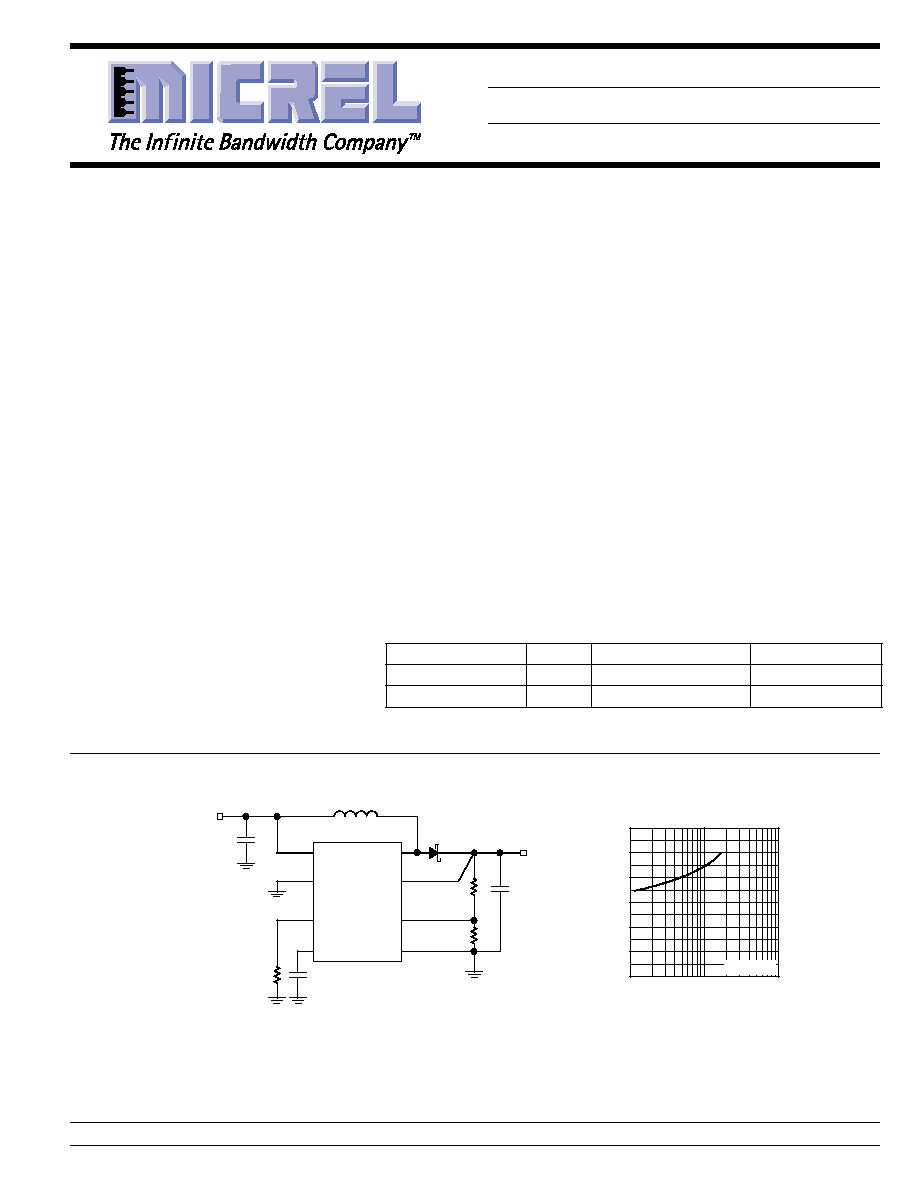
Typical Application
L1
10 H
D1
MIC2145BMM
RSET
PGND
EN
SW
V
OUT
10V/150mA
VDD
FB
SGND
I Limit
V
IN
3.0V to 5.0V
SS
C
IN
10 F/6.3V
C
OUT
10 F/16V
1
5
6
7
8
4
3
2
60
65
70
75
80
85
90
10
100
1000
EFFICIENCY (%)
OUTPUT CURRENT (mA)
10V Output
Efficiency
V
IN
= 3.0V
Adjustable Output Boost Converter with Programmable Peak Switch Current
Features
∑ 2.4V to 16V input voltage
∑ Output adjustable to 16V
∑ Programmable peak current limit
∑ Soft start
∑ Up to 450kHz switching frequency
∑ 0.5
µ
A shutdown current
∑ 200
µ
A quiescent current
∑ Capable of 5V/ 500mA output with 3.3V input
∑ Achieves over 85% efficiency
∑ Implements low power BOOST, SEPIC, and FLYBACK
topologies
∑ MSOP-8 and 3mm
◊
3mm MLFTM-10L
Applications
∑ Flash LED driver
∑ LCD bias supply
∑ White LED driver
∑ DSL bias supply
∑ Local 3V to 5V conversion
Micrel, Inc. ∑ 1849 Fortune Drive ∑ San Jose, CA 95131 ∑ USA ∑ tel + 1 (408) 944-0800 ∑ fax + 1 (408) 944-0970 ∑ http://www.micrel.com
Ordering Information
Part Number
Voltage
Ambient Temp. Range
Package
MIC2145BMM
Adj
≠40
∞
C to +85
∞
C
8-lead MSOP
MIC2145BML
Adj
≠40
∞
C to +85
∞
C
3
◊
3 MLFTM-10L

MIC2145
Micrel
MIC2145
2
May 2003
Pin Description
Pin Number
Pin Number
Pin Name
Pin Function
MSOP
MLF
1
1
EN
Enable (Input): Logic high (
1.5V) enables regulator. Logic low (
0.7V)
shuts down regulator. Do not float.
2
2
SS
Soft Start Capacitor (External Component): Connect external capacitor to
ground to control the rise time of the output voltage.
3
3
RSET
Current Limit (External Component): Sets peak current limit of the internal
power MOSFET using an external resistor.
4
4, 5
PGND
Power Ground (Return): Internal power MOSFET source.
5
6, 7
SW
Switch Node (Input): Internal power MOSFET drain.
6
8
VDD
Supply (Input): +2.4V to +16V for internal circuitry.
7
9
FB
Feedback (Input): Output voltage sense node.
8
10
SGND
Small Signal Ground (Return): Ground
Pin Configuration
1
EN
SS
RSET
PGND
8
SGND
FB
VDD
SW
7
6
5
2
3
4
8-Lead MSOP (MM)
EN
SS
RSET
PGND
SGND
FB
VDD
SW
1
2
3
4
10
9
8
7
5
6
PGND
SW
3mm
◊◊
◊◊
◊
3mm MLF-10L (ML)
May 2003
3
MIC2145
MIC2145
Micrel
Electrical Characteristics
(Note 6)
V
DD
= 10V, V
OUT
= 10V, I
OUT
= 100mA; T
J
=25
∞
C, unless otherwise noted, bold values indicate ≠40
∞
C
T
J
125
∞
C.
Parameter
Condition
Min
Typ
Max
Units
Supply Voltage
2.4
16
V
Shutdown Current
EN = 0.3V, V
DD
= 10V, V
FB
=1.35V
0.5
5
µ
A
Quiescent Current
EN = V
DD
, V
DD
= 10V, V
FB
= 1.35V
200
300
µ
A
Feedback Voltage Reference
(
±
2%)
1.058
1.08
1.102
V
(
±
3%)
1.048
1.112
V
Comparator Hysteresis
18
mV
Feedback Input Current
V
FB
=1.35V
40
nA
Peak Current Limit
R
SET
=200
, V
DD
= 3.6V, Note 4
0.8
A
R
SET
=1k
, V
DD
= 10V, Note 4
0.9
A
Current Limit Comparator
500
ns
Propagation Delay
Switch On-Resistance
I
SW
= 150mA, V
DD
= 3.0V
500
750
m
I
SW
= 1.2A, V
DD
= 10V
250
400
m
Maximum Off Time
1000
ns
Enable Input Voltage
Logic Low (turn-off)
1.1
0.7
V
Logic High (turn-on)
1.5
1.1
V
Enable Input Current
V
EN
= 0V
≠1
0.01
1
µ
A
V
EN
= 2V
≠1
0.01
1
µ
A
Soft Start Current
V
EN
= 2V, V
DD
=3.0V
≠8
≠12
≠16
µ
A
Note 1.
Exceeding the absolute maximum rating may damage the device.
Note 2.
The device is not guaranteed to function outside its operating rating.
Note 3.
Devices are ESD sensitive. Handling precautions recommended. Human body model, 1.5K
in series with 100pF.
Note 4.
The current is measured in a DC mode. Actual peak switching current will be higher due to internal propagation delay of the circuit.
Note 5.
V
EN
V
DD
.
Note 6.
Specification for packaged product only.
Absolute Maximum Ratings
(Note 1)
Supply Voltage (V
DD
) .................................................... 18V
Switch Voltage (V
SW
) .................................................... 18V
Feedback Voltage (V
FB
) ................................................ 18V
Switch Current (I
SW
) ........................................................ 2A
Enable Voltage(V
EN
), Note 5 ........................................ 18V
RSET Voltage (V
RSET
) .................................................... 6V
ESD Rating, Note 3 ...................................................... 2kV
Ambient Storage Temperature(T
S
) .......... ≠65
∞
C to +150
∞
C
Operating Ratings
(Note 2)
Supply Voltage (V
DD
) ....................................... 2.4V to 16V
Switch Voltage (V
SW
) .................................................... 16V
Ambient Temperature (T
A
) ......................... ≠40
∞
C to +85
∞
C
Junction Temperature (T
J
) ....................... ≠40
∞
C to +125
∞
C
Package Thermal Resistance MSOP
JA
(MSOP-8) .................................................... 206
∞
C/W
JA
(3mm
◊
3mm MLF-10) .................................... 60
∞
C/W
MIC2145
Micrel
MIC2145
4
May 2003
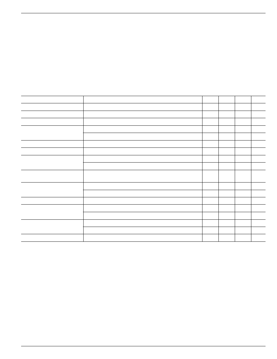
Typical Characteristics
50
60
70
80
90
100
0
0.01
0.02
0.03
0.04
0.05
0.06
0.07
0.08
EFFICIENCY (%)
OUTPUT CURRENT (A)
Efficiency-Basic
Configuration
V
IN
= 3.3V
V
OUT
= 10V
L = 10
µ
H
50
60
70
80
90
100
0
0.01
0.02
0.03
0.04
0.05
0.06
0.07
0.08
EFFICIENCY (%)
OUTPUT CURRENT (A)
Efficiency-Bootstrapped
Configuration
V
IN
=
3.3V
V
OUT
=
10V
L
=
10
µ
H
9.2
9.4
9.6
9.8
10.0
10.2
0
0.01
0.02
0.03
0.04
0.05
0.06
0.07
0.08
0.09
V
OUT
(V)
OUTPUT CURRENT (A)
Load Regulation
V
IN
= 3.6V
L = 10
µ
H
14.0
14.2
14.4
14.6
14.8
15.0
15.2
15.4
15.6
15.8
16.0
2
4
6
8
10
12
14
16
V
OUT
(V)
V
DD
(V)
Line Regulation
L = 10
µ
H
I
OUT
= 10mA
0.0
0.1
0.2
0.3
0.4
0.5
0.6
0.7
0.8
0.9
1.0
0
2
4
6
8 10 12 14 16 18
SWITCH ON-RESISTANCE (
)
V
DD
(V)
Switch On-Resistance
vs. V
DD
0.00
0.05
0.10
0.15
0.20
0.25
0.30
0.35
0.40
0.45
0.50
0
2
4
6
8 10 12 14 16 18
QUIESCENT CURRENT (
)
V
DD
(V)
Quiescent Current
vs. V
DD
1.05
1.06
1.07
1.08
1.09
1.1
-40 -20
0
20
40
60
80 100
FEEDBACK VOLTAGE (V)
TEMPERATURE (
∞
C)
Feedback Voltage
vs. Temperature
0.00
0.01
0.02
0.03
0.04
0.05
0.06
0.07
0.08
0.09
0.10
-40 -20
0
20
40
60
80 100
FEEDBACK CURRENT (
µ
A)
TEMPERATURE (
∞
C)
Feedback Current
vs. Temperature
0.5
0.6
0.7
0.8
0.9
1.0
1.1
1.2
1.3
1.4
1.5
-40 -20
0
20
40
60
80 100
OFF TIME (
µ
s)
TEMPERATURE (
∞
C)
Off Time
vs. Temperature
0.00
0.05
0.10
0.15
0.20
0.25
0.30
0.35
0.40
0.45
0.50
-40 -20
0
20
40
60
80 100
SHUTDOWN CURRENT (
µ
A)
TEMPERATURE (
∞
C)
Shutdown Current
vs. Temperature
0.00
0.05
0.10
0.15
0.20
0.25
0.30
0.35
0.40
0.45
0.50
-40 -20
0
20
40
60
80 100
QUIESCENT CURRENT (mA)
TEMPERATURE (
∞
C)
Quiescent Current
vs. Temperature
V
IN
= 3.6V
0.0
0.1
0.2
0.3
0.4
0.5
0.6
0.7
0.8
0.9
1.0
-40 -20
0
20
40
60
80 100
SWITCH ON-RESISTANCE (
)
TEMPERATURE (
∞
C)
Switch On-Resistance
vs. Temperature
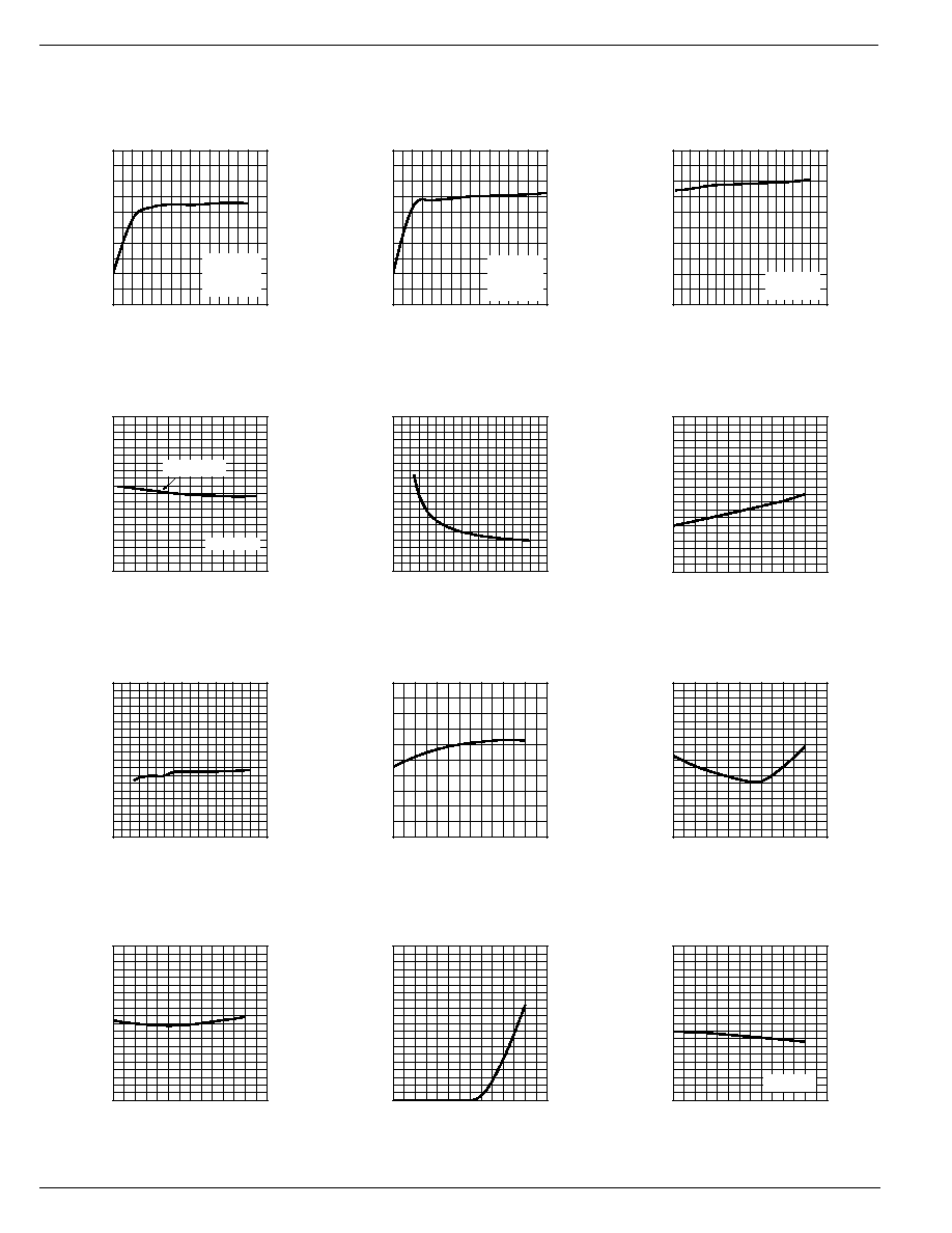
May 2003
5
MIC2145
MIC2145
Micrel
0
0.1
0.2
0.3
0.4
0.5
0.6
0.7
0.8
0.9
1.0
1.1
1.2
1.3
1.4
-40 -20
0
20
40
60
80 100
PEAK CURRENT LIMIT (A)
TEMPERATURE (
∞
C)
Peak Current Limit
vs. Temperature
V
IN
= 3.6V
V
OUT
= 10V
L = 10
µ
H
R
SET
= 200
R
SET
= 500
R
SET
= 1k
R
SET
= 10k
0
2
4
6
8
10
12
14
-40 -20
0
20
40
60
80 100
SOFT START CURRENT (
µ
A)
TEMPERATURE (
∞
C)
Soft Start Current
vs. Temperature
V
IN
= 3.6V
400
600
800
1000
1200
1400
1600
1800
2000
100
1000
10000
100000
PEAK CURRENT LIMIT (mA)
RSET(
)
Peak Current Limit
vs. RSET
15V
5.0V
4.2V
2.4V
3.0V
3.3V
3.6V
8.0V
10V
12V
VOUT/VIN > 1.25
L = 10
µ
H
VIN =
MIC2145
Micrel
MIC2145
6
May 2003
Functional Diagram
SGND
V
IN
VDD
R1
C
OUT
C
FF
C
IN
D1
10
µ
H
L1
V
OUT
R2
PGND
FB
Current Limit
Comparator
Feedback
Comparator
POWER
MOSFET
One Shot
800nS
/S
EN
SW
RSET
SS
/R
/Q
Thermal
Shutdown
On(/Off)
6
3
2
1
7
4
8
5
C
SS
V
REF
R
SET
Soft
Start
1
R1
R2
+
V
1.08
OUT
=
Figure 1. Block Diagram

May 2003
7
MIC2145
MIC2145
Micrel
Functional Description
See
"Application Information"
for component selection and
pre-designed circuits.
Overview
The MIC2145 is a 2.5W boost regulator with programmable
peak current limit and a constant off time. Quiescent current
for the MIC2145 is typically 200
µ
A when the switch is in the
off state. Efficiencies above 80% throughout most operating
conditions can be realized.
Regulation
Regulation is achieved by both of the comparators, which
regulate the inductor current and the output voltage by gating
the power MOSFET. Initially, power is applied to the SW and
VDD pins. When the part is enabled, the power MOSFET
turns on and current flows. When the current exceeds the
peak current limit threshold, the current limit comparator fires
the one-shot to turn off the power MOSFET for 1000ns and
resets the SR flip-fop. The current limit comparator continues
to cycle the power MOSFET on and off until the output voltage
trips the upper threshold of the feedback comparator, which
terminates the cycle. The cycle will begin again when the
output voltage drops below the lower hysteresis threshold of
the feedback comparator. The feedback comparator has a
typical hysteresis of 18mV. Due to the gain of the feedback
resistor divider, the voltage at V
OUT
experiences a typical
167mV of hysteresis for 10V output at 2.4V V
DD
. This can be
reduced by adding a feed-forward capacitor, C
FF
(See
"Output Voltage"
section).
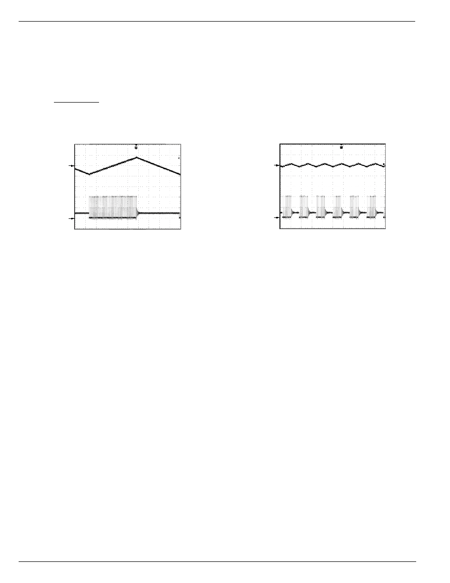
Time 20
µ
s
V
OUT
AC Couple
(100mV/div)
V
SW
(5V/div)
I
INDUCTOR
(500mA/div)
Figure 2. Typical Regulator Waveforms
Output
The maximum output voltage is limited by the voltage capa-
bility of the output switch. Output voltages of up to 16V can be
achieved with the boost circuit. Higher output voltages re-
quire a flyback configuration.
Peak Current Limit
The peak current limit is externally set with a resistor. The
peak current range is from 420mA to 2A. There is a minimum
resistor value for R
SET
at lower V
DD
voltages. For resistor
value selections, see the
"Typical Characteristics: Peak
Current Limit vs. R
SET
"
.
Soft Start
The MIC2145 has a built in soft start that controls the rise time
of the output voltage and the peak current limit threshold
during start up.
Time 200
µ
s
V
OUT
(5V/div)
V
EN
(2V/div)
V
SW
(5V/div)
I
INDUCTOR
(500mA/div)
V
IN
= 3V
V
OUT
= 10V
R
SET
= 10k
C
SS
= 0.01
µ
F
Figure 3. Typical Soft Start Waveforms
Thermal Shutdown
Built-in thermal protection circuitry turns off the power MOSFET
when the junction temperature exceeds about 150
∞
C.
MIC2145
Micrel
MIC2145
8
May 2003
Application Information
Pre-designed circuit information is at the end of this section.
Output Voltage
The output voltage of the regulator can be set between 2.4V
and 16V by connecting a resistor divider at the FB pin. The
resistor values are selected by the following equations:
R
V R
V
V
OUT
2
1 08
1
1 08
=
-
.
∑
.
Time 20
µ
s
V
OUT
AC Couple
(100mV/div)
V
SW
(5V/div)
Figure 4. Without Feed-Forward Capacitor
Time 4
µ
s
V
OUT
AC Couple
(100mV/div)
V
SW
(5V/div)
Figure 5. With Feed-Forward Capacitor (100pF)
A value of 1M
is recommended for R1 to minimize the
quiescent current when the part is off. Then, R2 can be solved
using the above equation. A feed-forward capacitor, C
FF
,
ranging from 5pF to 100pF can be used in parallel with R1 to
reduce the peak-to-peak output voltage ripple, which is
shown in Figures 4 and 5.
May 2003
9
MIC2145
MIC2145
Micrel
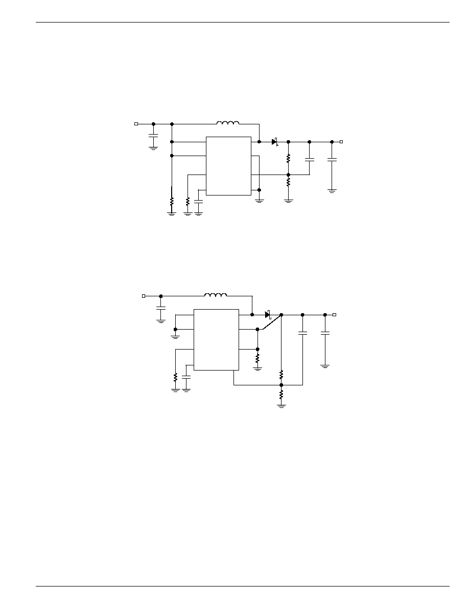
Bootstrap
A bootstrapped configuration is recommended for applica-
tions that require high efficiency at heavy loads (>70mA).
This is achieved by connecting the V
DD
pin to V
OUT
(see
L1
10
µ
H
Sumida
CR43-100
MIC2145
D1
On Semiconductor
MBR0530T1
RSET
EN
VDD
SW
R4
1M
R3
274k
C3
100pF
V
OUT
5V/250mA
PGND
FB
SGND
R1
100k
V
IN
3.6V
SS
C2
0.01
µ
F
C1
10
µ
F/6.3V
Murata
GRM42-6 X5R 106K 6.3
R2
10k
C4
10
µ
F/6.3V
Murata
GRM42-6 X5R 106K 6.3
Figure 6. Basic Configuration
L1
10
µ
H
Sumida
CR43-100
MIC2145
D1
On Semiconductor
MBR0530T1
RSET
SGND
PGND
SW
R4
1M
R1
100k
C3
100pF
V
OUT
5V/350mA
VDD
EN
FB
V
IN
3.6V
SS
C2
0.01
µ
F
C1
10
µ
F/6.3V
Murata
GRM42-6 X5R 106K 6.3
R2
10k
R3
274k
C4
10
µ
F/6.3V
Murata
GRM42-6 X5R 106K 6.3
Figure 7. Bootstrap Configuration
Figure 7). For applications that require high efficiency at light
loads (<70mA), the V
DD
pin is connected to the input voltage
(V
IN
); this is referred to as the basic configuration (see Figure
6).

MIC2145
Micrel
MIC2145
10
May 2003
Inductor
The MIC2145 has a programmable peak current to allow the
usage of small surface mount inductors. A 10
µ
H or 4.7
µ
H
inductor is recommended for most portable applications such
as powering white LEDs and biasing LCD panels. The
inductor should have a saturation current rating higher than
the peak current during circuit operation. A low ESR (Equiva-
lent Series Resistance) inductor is also desirable for high
efficiency. Below are tables that list the maximum output
current at minimum input voltage with efficiencies greater
than 80%.
V
)
n
i
m
(
N
I
V
)
x
a
m
(
N
I
T
E
S
R
I
)
x
a
m
(
T
U
O
V
T
U
O
)
V
(
)
V
(
)
(
)
A
m
(
)
V
(
0
.
3
5
.
4
0
0
4
0
5
2
5
5
.
9
0
8
0
1
5
.
9
0
6
2
1
5
.
9
0
5
5
1
Table 3. Typical Application for 4.7
µ
H Inductor in
Basic Configuration
V
)
n
i
m
(
N
I
V
)
x
a
m
(
N
I
T
E
S
R
I
)
x
a
m
(
T
U
O
V
T
U
O
)
V
(
)
V
(
)
(
)
A
m
(
)
V
(
0
.
3
5
.
4
0
0
2
0
0
5
5
5
.
4
5
2
2
0
1
5
.
4
0
5
1
2
1
5
.
4
0
3
1
5
1
Table 4. Typical Application for 4.7
µ
H Inductor in
Bootstrap Configuration
V
)
n
i
m
(
N
I
V
)
x
a
m
(
N
I
T
E
S
R
I
)
x
a
m
(
T
U
O
V
T
U
O
)
V
(
)
V
(
)
(
)
A
m
(
)
V
(
4
.
2
5
.
4
k
0
1
0
8
5
5
.
9
5
2
0
1
5
.
1
1
0
2
2
1
5
.
4
1
5
1
5
1
0
.
3
5
.
4
k
0
1
0
5
1
5
5
.
9
0
5
0
1
5
.
1
1
0
4
2
1
5
.
4
1
0
3
5
1
6
.
3
5
.
4
k
0
1
0
5
2
5
5
.
9
0
7
0
1
5
.
1
1
0
5
2
1
5
.
4
1
0
4
5
1
0
.
5
5
.
9
k
0
1
0
9
1
0
1
5
.
1
1
0
3
1
2
1
5
.
4
1
0
9
5
1
Table 1. Typical Application for 10
µ
H Inductor in
Basic Configuration
V
)
n
i
m
(
N
I
V
)
x
a
m
(
N
I
T
E
S
R
I
)
x
a
m
(
T
U
O
V
T
U
O
)
V
(
)
V
(
)
(
)
A
m
(
)
V
(
4
.
2
5
.
4
k
0
1
0
6
1
5
5
.
9
0
0
1
0
1
5
.
1
1
0
9
2
1
5
.
4
1
0
7
5
1
0
.
3
5
.
4
k
0
1
0
5
2
5
5
.
9
0
5
1
0
1
5
.
1
1
0
2
1
2
1
5
.
4
1
0
0
1
5
1
6
.
3
5
.
4
k
0
1
0
5
3
5
5
.
9
0
7
1
0
1
5
.
1
1
0
5
1
2
1
5
.
4
1
0
2
1
5
1
0
.
5
5
.
9
k
0
1
0
0
3
0
1
5
.
1
1
0
5
2
2
1
5
.
4
1
0
0
2
5
1
Table 2. Typical Application for 10
µ
H Inductor in
Bootstrap Configuration

May 2003
11
MIC2145
MIC2145
Micrel
Diode
A Schottky diode should be used for the output diode. Most
of the application circuits on this data sheet specify the
Motorola MBR0530 surface mount Schottky diode. It has a
forward current of 0.5A and a low forward voltage drop. For
applications that are cost driven, the 1N4148 or equivalent
can be used but the efficiency will suffer due to higher forward
voltage drop.
Output Capacitor
Low ESR capacitors should be used at the output of the
MIC2145 to minimize the switching output ripple voltage.
Selection of the capacitor value will depend upon the peak
inductor current, inductor size, and the load. MuRata offers
the GRM43-2 series with up to 10
µ
F at 25V, with a X5R
temperature coefficient in a 1812 surface-mount package.
For lower output voltage applications, the GRM42-2 (1210
package/10
µ
F/16V) and GRM42-6 (1206 package/10
µ
F/
6.3V) series can be used. Typically, values ranging from
10
µ
F to 47
µ
F can be used for the output capacitor.
Reducing Peak Current
If lower than 400mA peak current is required then the soft
start pin may be shorted to ground. This changes the refer-
ence of the current limit comparator. With the soft start pin
shorted to ground, the maximum current will approximately
reduce to half. The peak current should always be set at least
50% higher than the maximum load current.
MIC2145
Micrel
MIC2145
12
May 2003
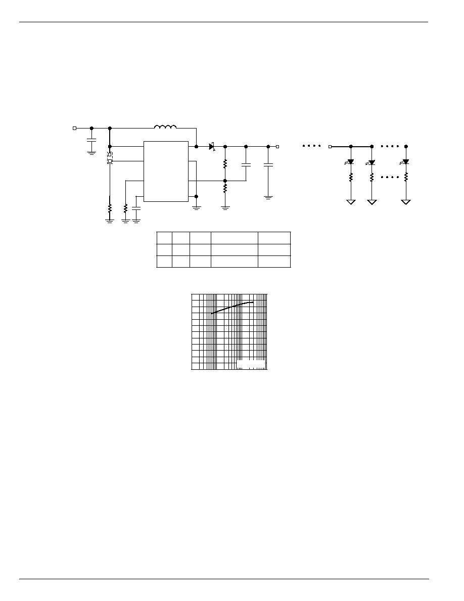
Pre-designed Application Circuits
L1
4.7
µ
H
Murata
LQH3C4R7M24
MIC2145
D1
On Semiconductor
MBR0530T1
RSET
EN
VDD
SW
R4
1M
R3
274k
C3
100pF
V
OUT
5V
PGND
FB
SGND
R1
100k
JP1
V
IN
3.0V-4.2V
SS
C2
0.01
µ
F
C1
10
µ
F/6.3V
Murata
GRM42-6 X5R 106K 6.3
R2
10k
C4
10
µ
F/6.3V
Murata
GRM42-6 X5R 106K 6.3
LED1
R
R
R
LED2
LEDn
V
N
I
V
T
U
O
d
a
o
L
e
g
a
t
l
o
V
e
l
p
p
i
R
y
c
n
e
i
c
i
f
f
E
V
V
A
m
)
k
a
e
p
-
k
a
e
p
(
V
m
%
6
.
3
0
.
5
0
4
0
0
1
<
5
8
60
65
70
75
80
85
90
1
10
100
1000
EFFICIENCY (%)
OUTPUT CURRENT (mA)
5V Output
Efficiency
V
IN
= 3.6V
Figure 8. White LED Driver Application (Drives 1 to 10 LEDs in Parallel)

May 2003
13
MIC2145
MIC2145
Micrel
L1
10
µ
H
Sumida
CR32-100
MIC2145
D1
On Semiconductor
MBR0530T1
RSET
EN
PGND
SW
R4
1M
R3
121k
C3
100pF
V
OUT
10.0V
VDD
FB
SGND
R1
100k
JP1
V
IN
3.0V-5.0V
SS
C2
0.01
µ
F
C1
10
µ
F/6.3V
Murata
GRM42-6 X5R 106K 6.3
R2
10k
C4
10
µ
F/16V
Murata
GRM42-2 X5R 106K 16
V
N
I
V
T
U
O
d
a
o
L
e
g
a
t
l
o
V
e
l
p
p
i
R
y
c
n
e
i
c
i
f
f
E
V
V
A
m
)
k
a
e
p
-
k
a
e
p
(
V
m
%
0
.
3
0
.
0
1
0
5
1
0
0
2
<
3
8
60
65
70
75
80
85
90
10
100
1000
EFFICIENCY (%)
OUTPUT CURRENT (mA)
10V Output
Efficiency
V
IN
= 3.0V
Figure 9. LCD Application -- Bootstrap Configuration

MIC2145
Micrel
MIC2145
14
May 2003
L1
10 H
Sumida
CR32-100
MIC2145
D1
On Semiconductor
MBR0530T1
RSET
EN
PGND
SW
R4
1M
R3
78.7k
C3
100pF
V
OUT
15.0V
LED1
R
LED2 LED3 LED4
VDD
FB
SGND
R1
100k
JP1
V
IN
3.0V-5.0V
SS
C2
0.01 F
C1
10 F/6.3V
Murata
GRM42-6 X5R 106K 6.3
R2
10k
C4
10 F/16V
Murata
GRM42-2 X5R 106K 16
V
N
I
V
T
U
O
d
a
o
L
e
g
a
t
l
o
V
e
l
p
p
i
R
y
c
n
e
i
c
i
f
f
E
V
V
A
m
)
k
a
e
p
-
k
a
e
p
(
V
m
%
6
.
3
0
.
5
1
0
4
0
0
1
<
5
8
60
65
70
75
80
85
90
1
10
100
EFFICIENCY (%)
OUTPUT CURRENT (mA)
15V Output
Efficiency
V
IN
= 3.6V
Figure 10. Series White LED Driver Application
May 2003
15
MIC2145
MIC2145
Micrel
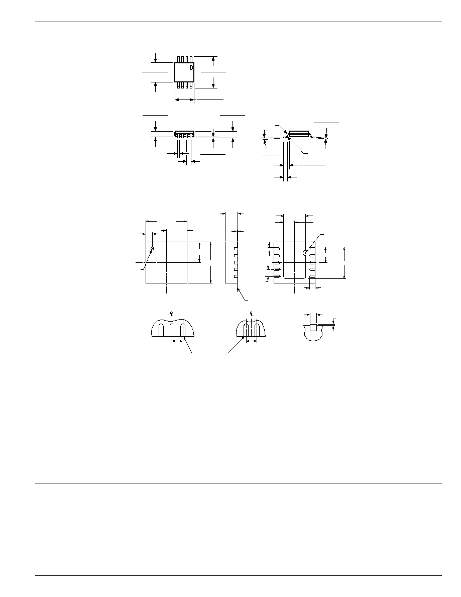
Package Information
0.008 (0.20)
0.004 (0.10)
0.039 (0.99)
0.035 (0.89)
0.021 (0.53)
0.012 (0.03) R
0.0256 (0.65) TYP
0.012 (0.30) R
5
∞
MAX
0
∞
MIN
0.122 (3.10)
0.112 (2.84)
0.120 (3.05)
0.116 (2.95)
0.012 (0.3)
0.007 (0.18)
0.005 (0.13)
0.043 (1.09)
0.038 (0.97)
0.036 (0.90)
0.032 (0.81)
DIMENSIONS:
INCH (MM)
0.199 (5.05)
0.187 (4.74)
8-Pin MSOP (MM)
0.20 dia
0.48 typ.
3.00 BSC.
1.50 BSC.
PIN 1 ID
0.85
3.00 BSC.
TOP
BOTTOM
ODD TERMINAL SIDE
EVEN TERMINAL SIDE
TERMINAL TIP
TERMINAL TIP
1.50 BSC.
1
2
3
1
2
3
--0.05
+0.15
0.01
0.50 BSC.
0.50 BSC.
0.50 BSC.
--0.01
+0.04
0.23
--0.05
+0.07
0.23
--0.05
+0.07
0.01
--0.01
+0.04
0.40
--0.05
+0.15
1.60
--0.15
+0.15
0.80
--0.15
+0.15
2.30
--0.15
+0.15
1.15
--0.15
+0.15
SEATING PLANE
10-Pin MLF (ML)
MICREL, INC.
1849 FORTUNE DRIVE
SAN JOSE, CA 95131
USA
TEL
+ 1 (408) 944-0800
FAX
+ 1 (408) 944-0970
WEB
http://www.micrel.com
The information furnished by Micrel in this datasheet is believed to be accurate and reliable. However, no responsibility is assumed by Micrel for its use.
Micrel reserves the right to change circuitry and specifications at any time without notification to the customer.
Micrel Products are not designed or authorized for use as components in life support appliances, devices or systems where malfunction of a product can
reasonably be expected to result in personal injury. Life support devices or systems are devices or systems that (a) are intended for surgical implant into
the body or (b) support or sustain life, and whose failure to perform can be reasonably expected to result in a significant injury to the user. A Purchaser's
use or sale of Micrel Products for use in life support appliances, devices or systems is at Purchaser's own risk and Purchaser agrees to fully indemnify
Micrel for any damages resulting from such use or sale.
© 2003 Micrel, Incorporated.