 | –≠–ª–µ–∫—Ç—Ä–æ–Ω–Ω—ã–π –∫–æ–º–ø–æ–Ω–µ–Ω—Ç: MIC2169 | –°–∫–∞—á–∞—Ç—å:  PDF PDF  ZIP ZIP |
November 2003
1
M9999-111803
MIC2169
Micrel
MIC2169
500kHz PWM Synchronous Buck Control IC
General Description
The MIC2169 is a high-efficiency, simple to use 500kHz
PWM synchronous buck control IC housed in a small MSOP-
10 package. The MIC2169 allows compact DC/DC solutions
with a minimal external component count and cost.
The MIC2169 operates from a 3V to 14.5V input, without the
need of any additional bias voltage. The output voltage can
be precisely regulated down to 0.8V. The adaptive all
N-Channel MOSFET drive scheme allows efficiencies over
95% across a wide load range.
The MIC2169 senses current across the high-side N-Chan-
nel MOSFET, eliminating the need for an expensive and
lossy current-sense resistor. Current limit accuracy is main-
tained by a positive temperature coefficient that tracks the
increasing R
DS(ON)
of the external MOSFET. Further cost
and space are saved by the internal in-rush-current limiting
digital soft-start.
The MIC2169 is available in a 10-pin MSOP package, with a
wide junction operating range of ≠40
∞
C to +125
∞
C.
All support documentation can be found on Micrel's web
site at www.micrel.com.
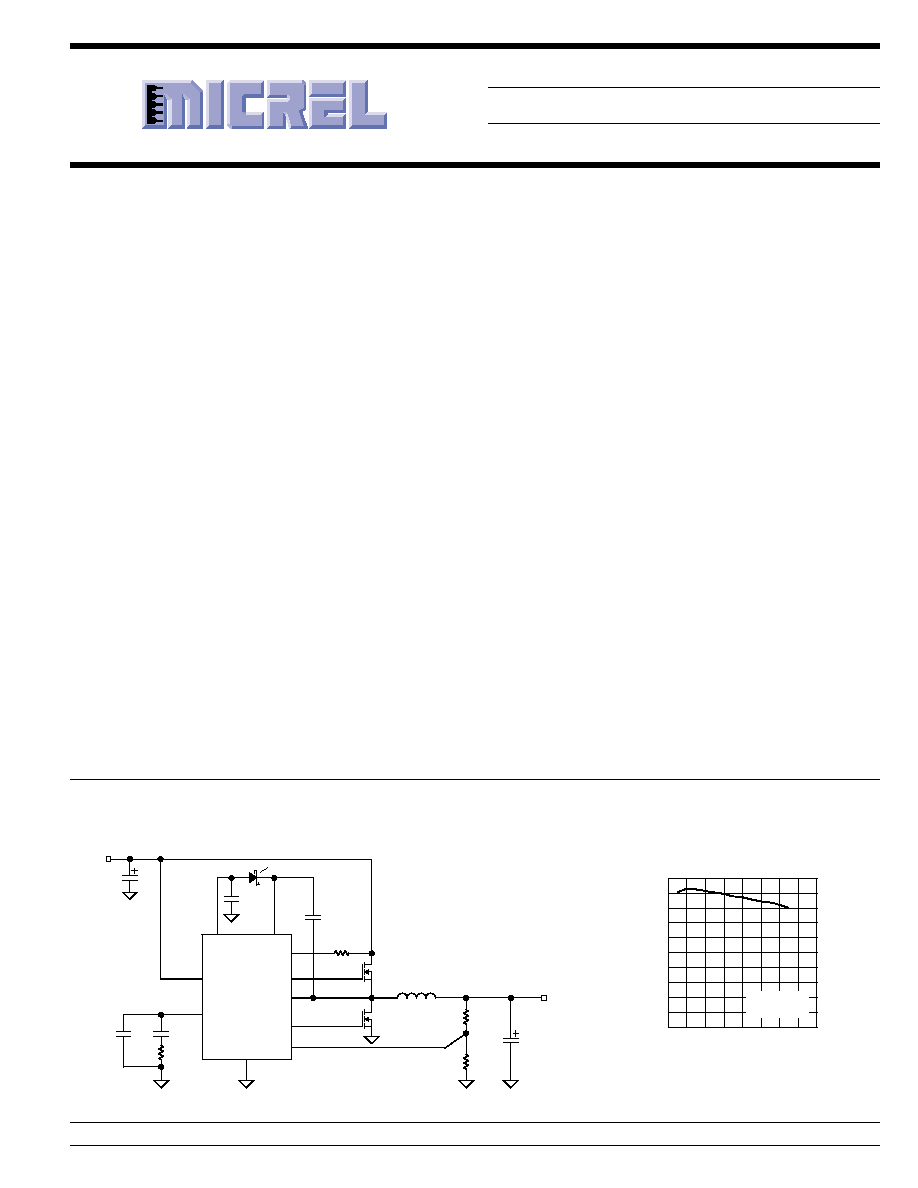
Typical Application
2.5
µ
H
3.3V
V
IN
= 5V
VDD
COMP/EN
VIN
CS
FB
GND
LSD
BST
1k
10k
4k
3.24k
4.7
µ
F
100
µ
F
0.1
µ
F
100nF
IRF7821
SD103BWS
IRF7821
150pF
HSD
VSW
MIC2169
150
µ
F x 2
MIC2169 Adjustable Output 500kHz Converter
Features
∑ 3V to 14.5V input voltage range
∑ Adjustable output voltage down to 0.8V
∑ Up to 95% efficiency
∑ 500kHz PWM operation
∑ Adjustable current limit senses high-side N-Channel
MOSFET current
∑ No external current-sense resistor
∑ Adaptive gate drive increases efficiency
∑ Ultra-fast response with hysteretic transient recovery
mode
∑ Overvoltage protection protects the load in fault
conditions
∑ Dual mode current limit speeds up recovery time
∑ Hiccup mode short-circuit protection
∑ Internal soft-start
∑ Dual function COMP and EN pin allows low-power
shutdown
∑ Small size MSOP 10-lead package
Applications
∑ Point-of-load DC/DC conversion
∑ Set-top boxes
∑ Graphic cards
∑ LCD power supplies
∑ Telecom power supplies
∑ Networking power supplies
∑ Cable modems and routers
Micrel, Inc. ∑ 1849 Fortune Drive ∑ San Jose, CA 95131 ∑ USA ∑ tel + 1 (408) 944-0800 ∑ fax + 1 (408) 944-0970 ∑ http://www.micrel.com
50
55
60
65
70
75
80
85
90
95
100
0
2
4
6
8
10 12 14 16
EFFICIENCY (%)
I
LOAD
(A)
MIC2169 Efficiency
V
IN
= 5V
V
OUT
= 3.3V

MIC2169
Micrel
M9999-111803
2
November 2003
Pin Configuration
FB
GND
6
5
1
VIN
VDD
CS
COMP/EN
10 BST
HSD
VSW
LSD
9
8
7
2
3
4
10-Pin MSOP (MM)
Pin Description
Pin Number
Pin Name
Pin Function
1
VIN
Supply Voltage (Input): 3V to 14.5V.
2
VDD
5V Internal Linear Regulator (Output): V
DD
is the external MOSFET gate
drive supply voltage and an internal supply bus for the IC. When V
IN
is <5V,
this regulator operates in dropout mode.
3
CS
Current Sense / Enable (Input): Current-limit comparator noninverting input.
The current limit is sensed across the MOSFET during the ON time. The
current can be set by the resistor in series with the CS pin.
4
COMP/EN
Compensation (Input): Dual function pin. Pin for external compensation. If
this pin is pulled below 0.2V, with the reference fully up the device shuts
down (50
µ
A typical current draw).
5
FB
Feedback (Input): Input to error amplifier. Regulates error amplifier to 0.8V.
6
GND
Ground (Return).
7
LSD
Low-Side Drive (Output): High-current driver output for external synchro-
nous MOSFET.
8
VSW
Switch (Return): High-side MOSFET driver return.
9
HSD
High-Side Drive (Output): High-current output-driver for the high-side
MOSFET. When V
IN
is between 3.0V to 5V, 2.5V threshold MOSFETs
should be used. At V
IN
> 5V, 5V threshold MOSFETs should be used.
10
BST
Boost (Input): Provides the drive voltage for the high-side MOSFET driver.
The gate-drive voltage is higher than the source voltage by V
IN
minus a
diode drop.
Ordering Information
Part Number
Frequency
Junction Temp. Range
Package
MIC2169BMM
500kHz
≠40
∞
C to +125
∞
C
10-lead MSOP

November 2003
3
M9999-111803
MIC2169
Micrel
Absolute Maximum Ratings
(1)
Supply Voltage (V
IN
) .................................................. 15.5V
Booststrapped Voltage (V
BST
) ............................... V
IN
+5V
Junction Temperature (T
J
) ................ ≠40
∞
C
T
J
+125
∞
C
Storage Temperature (T
S
) ....................... ≠65
∞
C to +150
∞
C
Operating Ratings
(2)
Supply Voltage (V
IN
) .................................... +3V to +14.5V
Output Voltage Range ........................... 0.8V to V
IN
◊
D
MAX
Package Thermal Resistance
JA
10-lead MSOP ............................................ 180
∞
C/W
Electrical Characteristics
(3)
T
J
= 25
∞
C, V
IN
= 5V; bold values indicate ≠40
∞
C < T
J
< +125
∞
C; unless otherwise specified.
Parameter
Condition
Min
Typ
Max
Units
Feedback Voltage Reference
(
±
1%)
0.792
0.8
0.808
V
Feedback Voltage Reference
(
±
2% over temp)
0.784
0.8
0.816
V
Feedback Bias Current
30
100
nA
Output Voltage Line Regulation
0.03
% / V
Output Voltage Load Regulation
0.5
%
Output Voltage Total Regulation
3V
V
IN
14.5V; 1A
I
OUT
10A; (V
OUT
= 2.5V)
(4)
0.6
%
Oscillator Section
Oscillator Frequency
450
500
550
kHz
Maximum Duty Cycle
92
%
Minimum On-Time
(4)
30
60
ns
Input and V
DD
Supply
PWM Mode Supply Current
V
CS
= V
IN
≠0.25V; V
FB
= 0.7V (output switching but excluding
1.5
3
mA
external MOSFET gate current.)
Shutdown Quiescent Current
V
COMP/EN
= 0V
50
150
µ
A
V
COMP
Shutdown Threshold
0.1
0.25
0.4
V
V
COMP
Shutdown Blanking
C
COMP
= 100nF
4
ms
Period
Digital Supply Voltage (V
DD
)
V
IN
6V
4.7
5
5.3
V
Notes:
1.
Absolute maximum ratings indicate limits beyond which damage to the component may occur. Electrical specifications do not apply when operating
the device outside of its operating ratings. The maximum allowable power dissipation is a function of the maximum junction temperature, T
J
(max),
the junction-to-ambient thermal resistance,
JA
, and the ambient temperature, T
A
. The maximum allowable power dissipation will result in excessive
die temperature, and the regulator will go into thermal shutdown.
2.
Devices are ESD sensitive, handling precautions required.
3.
Specification for packaged product only.
4.
Guaranteed by design.

MIC2169
Micrel
M9999-111803
4
November 2003
Parameter
Condition
Min
Typ
Max
Units
Error Amplifier
DC Gain
70
dB
Transconductance
1
ms
Soft-Start
Soft-Start Current
After timeout of internal timer. See
"Soft-Start"
section.
8.5
µ
A
Current Sense
CS Over Current Trip Point
V
CS
= V
IN
≠0.25V
160
200
240
µ
A
Temperature Coefficient
+1800
ppm/
∞
C
Output Fault Correction Thresholds
Upper Threshold, V
FB_OVT
(relative to V
FB
)
+3
%
Lower Threshold, V
FB_UVT
(relative to V
FB
)
≠3
%
Gate Drivers
Rise/Fall Time
Into 3000pF at V
IN
> 5V
30
ns
Output Driver Impedance
Source, V
IN
= 5V
6
Sink, V
IN
= 5V
6
Source, V
IN
= 3V
10
Sink, V
IN
= 3V
10
Driver Non-Overlap Time
Note 6
10
20
ns
Notes:
5.
Specification for packaged product only.
6.
Guaranteed by design.
Electrical Characteristics
(5)

November 2003
5
M9999-111803
MIC2169
Micrel
Typical Characteristics
V
IN
= 5V
0.5
0.7
0.9
1.1
1.3
1.5
1.7
1.9
2.1
2.3
2.5
2.7
2.9
-40 -20 0 20 40 60 80 100120140
I
DD
(mA)
TEMPERATURE (
∞
C)
PWM Mode Supply Current
vs. Temperature
0.5
1.0
1.5
2.0
0
5
10
15
QUIESCENT CURRENT (mA)
SUPPLY VOLTAGE (V)
PWM Mode Supply Current
vs. Supply Voltage
0.7980
0.7985
0.7990
0.7995
0.8000
0.8005
0.8010
0
5
10
15
V
FB
(V)
V
IN
(V)
V
FB
Line Regulation
0.792
0.794
0.796
0.798
0.800
0.802
0.804
0.806
-60 -30
0
30
60
90 120 150
V
FB
(V)
TEMPERATURE (
∞
C)
V
FB
vs. Temperature
0
1
2
3
4
5
6
0
5
10
15
V
DD
(V)
V
IN
(V)
V
DD
Line Regulation
4.90
4.92
4.94
4.96
4.98
5.00
5.02
0
5
10
15
20
25
30
V
DD
REGULATOR VOLTAGE (V)
LOAD CURRENT (mA)
V
DD
Load Regulation
0.0
0.5
1.0
1.5
2.0
2.5
3.0
3.5
4.0
4.5
5.0
-60 -30
0
30
60
90 120 150
V
DD
LINE REGULATION (%)
TEMPERATURE (
∞
C)
V
DD
Line Regulation
vs. Temperature
450
460
470
480
490
500
510
520
530
540
550
-60 -30
0
30
60
90 120 150
FREQUENCY (kHz)
TEMPERATURE (
∞
C)
Oscillator Frequency
vs. Temperature
-1.5
-1.0
-0.5
0
0.5
1.0
1.5
0
5
10
15
FREQUENCY VARIATION (%)
V
IN
(V)
Oscillator Frequency
vs. Supply Voltage
0
1
2
3
4
0
2
4
6
8
10
V
OUT
(V)
I
LOAD
(A)
Current Limit Foldback
R
CS
= 1k
Top MOSFET = Si4800
100
120
140
160
180
200
220
240
260
-60 -30
0
30
60
90 120 150
I
CS
(
µ
A)
TEMPERATURE (
∞
C)
Overcurrent Trip Point
vs. Temperature
MIC2169
Micrel
M9999-111803
6
November 2003
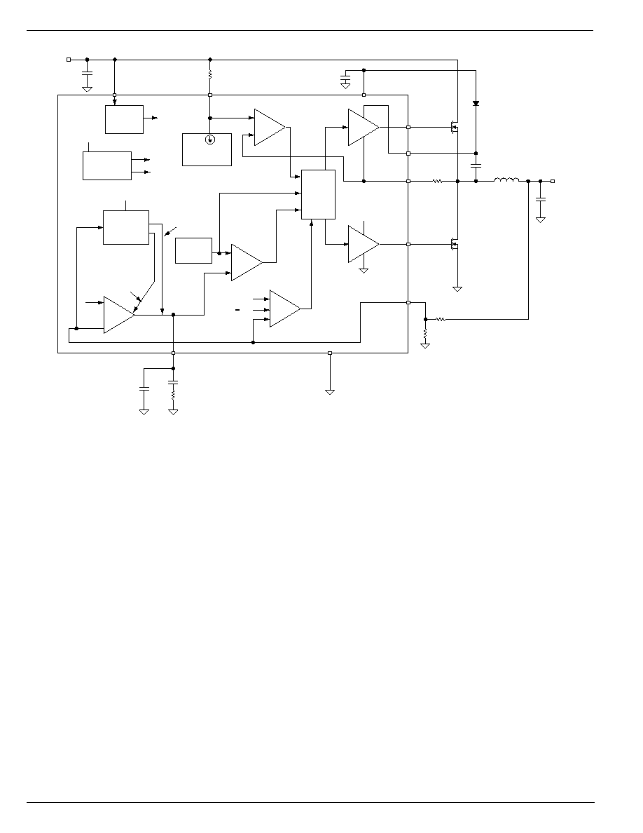
Functional Description
The MIC2169 is a voltage mode, synchronous step-down
switching regulator controller designed for high power with-
out the use of an external sense resistor. It includes an
internal soft-start function which reduces the power supply
input surge current at start-up by controlling the output
voltage rise time, a PWM generator, a reference voltage, two
MOSFET drivers, and short-circuit current limiting circuitry to
form a complete 500kHz switching regulator.
Theory of Operation
The MIC2169 is a voltage mode step-down regulator. The
figure above illustrates the block diagram for the voltage
control loop. The output voltage variation due to load or line
changes will be sensed by the inverting input of the
transconductance error amplifier via the feedback resistors
R3, and R2 and compared to a reference voltage at the non-
inverting input. This will cause a small change in the DC
voltage level at the output of the error amplifier which is the
input to the PWM comparator. The other input to the com-
parator is a 0 to 1V triangular waveform. The comparator
generates a rectangular waveform whose width t
ON
is equal
to the time from the start of the clock cycle t
0
until t
1
, the time
the triangle crosses the output waveform of the error ampli-
fier. To illustrate the control loop, let us assume the output
voltage drops due to sudden load turn-on, this would cause
Functional Diagram
Current Limit
Reference
Current Limit
Comparator
Error
Amp
Low-Side
Driver
High-Side
Driver
PWM
Comparator
FB
COMP
GND
LSD
V
REF
+3%
V
REF
3%
HSD
V
DD
C
BST
CS
V
DD
5V
5V
5V
C2
C1
R1
5V
0.8V
V
IN
SW
Q2
Q1
L1
Driver
Logic
0.8V
BG Valid
Clamp &
Startup
Current
Enable
Error
Loop
Hys
Comparator
5V LDO
Bandgap
Reference
Soft-Start &
Digital Delay
Counter
MIC2169
Ramp
Clock
BOOST
R2
R3
4
RSW
RCS
C
OUT
V
OUT
C
IN
D1
MIC2169 Block Diagram
the inverting input of the error amplifier which is divided down
version of V
OUT
to be slightly less than the reference voltage
causing the output voltage of the error amplifier to go high.
This will cause the PWM comparator to increase t
ON
time of
the top side MOSFET, causing the output voltage to go up
and bringing V
OUT
back in regulation.
Soft-Start
The COMP/EN pin on the MIC2169 is used for the following
three functions:
1. Disables the part by grounding this pin
2. External compensation to stabilize the voltage
control loop
3. Soft-start
For better understanding of the soft-start feature, let's as-
sume V
IN
= 12V, and the MIC2169 is allowed to power-up by
un-grounding the COMP/EN pin. The COMP pin has an
internal 6.5
µ
A current source that charges the external com-
pensation capacitor. As soon as this voltage rises to 180mV
(t = Cap_COMP
◊
0.18V/8.5
µ
A), the MIC2169 allows the
internal V
DD
linear regulator to power up and as soon as it
crosses the undervoltage lockout of 2.6V, the chip's internal
oscillator starts switching. At this point in time, the COMP pin
current source increases to 40
µ
A and an internal 11-bit
counter starts counting which takes approximately 2ms to
complete. During counting, the COMP voltage is clamped at
November 2003
7
M9999-111803
MIC2169
Micrel
0.65V. After this counting cycle the COMP current source is
reduced to 8.5
µ
A and the COMP pin voltage rises from 0.65V
to 0.95V, the bottom edge of the saw-tooth oscillator. This is
the beginning of 0% duty cycle and it increases slowly
causing the output voltage to rise slowly. The MIC2169 has
two hysteretic comparators that are enabled when V
OUT
is
within
±
3% of steady state. When the output voltage reaches
97% of programmed output voltage then the g
m
error ampli-
fier is enabled along with the hysteretic comparator. This
point onwards, the voltage control loop (g
m
error amplifier) is
fully in control and will regulate the output voltage.
Soft-start time can be calculated approximately by adding the
following four time frames:
t1 = Cap_COMP
◊
0.18V/8.5
µ
A
t2 = 12 bit counter, approx 2ms
t3 = Cap_COMP
◊
0.3V/8.5
µ
A
t4
V
V
0.5
Cap_COMP
8.5 A
OUT
IN
=
◊
◊
µ
Soft-Start Time(Cap_COMP=100nF) = t1 + t2 + t3 +
t4 = 2.1ms + 2ms + 3.5ms + 1.8ms = 10ms
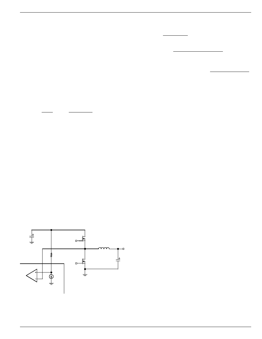
Current Limit
The MIC2169 uses the R
DS(ON)
of the top power MOSFET to
measure output current. Since it uses the drain to source
resistance of the power MOSFET, it is not very accurate. This
scheme is adequate to protect the power supply and external
components during a fault condition by cutting back the time
the top MOSFET is on if the feedback voltage is greater than
0.67V. In case of a hard short when feedback voltage is less
than 0.67V, the MIC2169 discharges the COMP capacitor to
0.65V, resets the digital counter and automatically shuts off
the top gate drive, and the g
m
error amplifier and the ≠3%
hysteretic comparators are completely disabled and the soft-
start cycles restarts. This mode of operation is called the
"hiccup mode" and its purpose is to protect the down stream
load in case of a hard short. The circuit in Figure 1 illustrates
the MIC2169 current limiting circuit.
L1 Inductor
V
IN
V
OUT
HSD
LSD
RCS
CS
200
µ
A
0
C2
C
IN
C1
C
OUT
Q1
MOSFET N
Q2
MOSFET N
Figure 1. The MIC2169 Current Limiting Circuit
The current limiting resistor R
CS
is calculated by the following
equation:
R
R
I
200 A
CS
DS(ON) Q1
L
=
◊
µ
Equation (1)
I
I
1
2 Inductor Ripple Current
L
LOAD
=
+
(
)
where:
Inductor Ripple Current = V
V
≠ V
V
F
L
OUT
IN
OUT
IN
SWITCHING
◊
(
)
◊
◊
F
SWITCHING
= 500kHz
200
µ
A is the internal sink current to program the MIC2169
current limit.
The MOSFET R
DS(ON)
varies 30% to 40% with temperature;
therefore, it is recommended to add a 50% margin to the load
current (I
LOAD
) in the above equation to avoid false current
limiting due to increased MOSFET junction temperature rise.
It is also recommended to connect R
CS
resistor directly to the
drain of the top MOSFET Q1, and the R
SW
resistor to the
source of Q1 to accurately sense the MOSFETs R
DS(ON)
. A
0.1
µ
F capacitor in parallel with R
CS
should be connected to
filter some of the switching noise.
Internal V
DD
Supply
The MIC2169 controller internally generates V
DD
for self
biasing and to provide power to the gate drives. This V
DD
supply is generated through a low-dropout regulator and
generates 5V from V
IN
supply greater than 5V. For supply
voltage less than 5V, the V
DD
linear regulator is approxi-
mately 200mV in dropout. Therefore, it is recommended to
short the V
DD
supply to the input supply through a 10
resistor for input supplies between 2.9V to 5V.
MOSFET Gate Drive
The MIC2169 high-side drive circuit is designed to switch an
N-Channel MOSFET. The block diagram in Figure 2 shows
a bootstrap circuit, consisting of D2 and CBST, supplies
energy to the high-side drive circuit. Capacitor CBST is
charged while the low-side MOSFET is on and the voltage on
the VSW pin is approximately 0V. When the high-side
MOSFET driver is turned on, energy from CBST is used to
turn the MOSFET on. As the MOSFET turns on, the voltage
on the VSW pin increases to approximately V
IN
. Diode D2 is
reversed biased and CBST floats high while continuing to
keep the high-side MOSFET on. When the low-side switch is
turned back on, CBST is recharged through D2. The drive
voltage is derived from the internal 5V V
DD
bias supply. The
nominal low-side gate drive voltage is 5V and the nominal
high-side gate drive voltage is approximately 4.5V due the
voltage drop across D2. An approximate 20ns delay between
the high- and low-side driver transitions is used to prevent
current from simultaneously flowing unimpeded through both
MOSFETs.
MOSFET Selection
The MIC2169 controller works from input voltages of 3V to
13.2V and has an internal 5V regulator to provide power to
turn the external N-Channel power MOSFETs for high- and

MIC2169
Micrel
M9999-111803
8
November 2003
low-side switches. For applications where V
IN
< 5V, the
internal V
DD
regulator operates in dropout mode, and it is
necessary that the power MOSFETs used are sub-logic level
and are in full conduction mode for V
GS
of 2.5V. For applica-
tions when V
IN
> 5V; logic-level MOSFETs, whose operation
is specified at V
GS
= 4.5V must be used.
It is important to note the on-resistance of a MOSFET
increases with increasing temperature. A 75
∞
C rise in junc-
tion temperature will increase the channel resistance of the
MOSFET by 50% to 75% of the resistance specified at 25
∞
C.
This change in resistance must be accounted for when
calculating MOSFET power dissipation and in calculating the
value of current-sense (CS) resistor. Total gate charge is the
charge required to turn the MOSFET on and off under
specified operating conditions (V
DS
and V
GS
). The gate
charge is supplied by the MIC2169 gate-drive circuit. At
500kHz switching frequency and above, the gate charge can
be a significant source of power dissipation in the MIC2169.
At low output load, this power dissipation is noticeable as a
reduction in efficiency. The average current required to drive
the high-side MOSFET is:
I
Q
f
G[high-side](avg)
G
S
=
◊
where:
I
G[high-side](avg)
= average high-side MOSFET gate
current.
Q
G
= total gate charge for the high-side MOSFET taken from
manufacturer's data sheet for V
GS
= 5V.
The low-side MOSFET is turned on and off at V
DS
= 0
because the freewheeling diode is conducting during this
time. The switching loss for the low-side MOSFET is usually
negligible. Also, the gate-drive current for the low-side
MOSFET is more accurately calculated using CISS at V
DS
=
0 instead of gate charge.
For the low-side MOSFET:
I
C
V
f
G[low-side](avg)
ISS
GS
S
=
◊
◊
Since the current from the gate drive comes from the input
voltage, the power dissipated in the MIC2169 due to gate
drive is:
P
V
I
I
GATEDRIVE
IN G[high-side](avg)
G[low-side](avg)
=
+
(
)
A convenient figure of merit for switching MOSFETs is the on
resistance times the total gate charge R
DS(ON)
◊
Q
G
. Lower
numbers translate into higher efficiency. Low gate-charge
logic-level MOSFETs are a good choice for use with the
MIC2169.
Parameters that are important to MOSFET switch selection
are:
∑ Voltage rating
∑ On-resistance
∑ Total gate charge
The voltage ratings for the top and bottom MOSFET are
essentially equal to the input voltage. A safety factor of 20%
should be added to the V
DS
(max) of the MOSFETs to account
for voltage spikes due to circuit parasitics.
The power dissipated in the switching transistor is the sum of
the conduction losses during the on-time (P
CONDUCTION
) and
the switching losses that occur during the period of time when
the MOSFETs turn on and off (P
AC
).
P
P
P
SW
CONDUCTION
AC
=
+
where:
P
I
R
CONDUCTION
SW(rms)
SW
2
=
◊
P
P
P
AC
AC(off)
AC(on)
=
+
R
SW
= on-resistance of the MOSFET switch
D
duty cycle
V
V
O
IN
=
Making the assumption the turn-on and turn-off transition
times are equal; the transition times can be approximated by:
t
C
V
C
V
I
T
ISS
GS
OSS
IN
G
=
◊
+
◊
where:
C
ISS
and C
OSS
are measured at V
DS
= 0
I
G
= gate-drive current (1A for the MIC2169)
The total high-side MOSFET switching loss is:
P
(V
V ) I
t
f
AC
IN
D
PK
T
S
=
+
◊
◊
◊
where:
t
T
= switching transition time (typically 20ns to 50ns)
V
D
= freewheeling diode drop, typically 0.5V
f
S
it the switching frequency, nominally 500kHz
The low-side MOSFET switching losses are negligible and
can be ignored for these calculations.
Inductor Selection
Values for inductance, peak, and RMS currents are required
to select the output inductor. The input and output voltages
and the inductance value determine the peak-to-peak induc-
tor ripple current. Generally, higher inductance values are
used with higher input voltages. Larger peak-to-peak ripple
currents will increase the power dissipation in the inductor
and MOSFETs. Larger output ripple currents will also require
more output capacitance to smooth out the larger ripple
current. Smaller peak-to-peak ripple currents require a larger
inductance value and therefore a larger and more expensive
inductor. A good compromise between size, loss and cost is
to set the inductor ripple current to be equal to 20% of the
maximum output current. The inductance value is calculated
by the equation below.
L
V
(V max
V
)
V max
f
0.2 I
max
OUT
IN
OUT
IN
S
OUT
=
◊
-
◊ ◊
◊
(
)
(
)
(
)
where:
f
S
= switching frequency, 500kHz
0.2 = ratio of AC ripple current to DC output current
V
IN
(max) = maximum input voltage

November 2003
9
M9999-111803
MIC2169
Micrel
The peak-to-peak inductor current (AC ripple current) is:
I
V
(V max
V
)
V max
f
L
PP
OUT
IN
OUT
IN
S
=
◊
-
◊ ◊
(
)
(
)
The peak inductor current is equal to the average output
current plus one half of the peak-to-peak inductor ripple
current.
I
I
max
0.5 I
PK
OUT
PP
=
+
◊
(
)
The RMS inductor current is used to calculate the I
2
◊
R
losses in the inductor.
I
I
max
1
1
3
I
I
max
INDUCTOR(rms)
OUT
P
OUT
2
=
◊
+
(
)
(
)
Maximizing efficiency requires the proper selection of core
material and minimizing the winding resistance. The high
frequency operation of the MIC2169 requires the use of ferrite
materials for all but the most cost sensitive applications.
Lower cost iron powder cores may be used but the increase
in core loss will reduce the efficiency of the power supply. This
is especially noticeable at low output power. The winding
resistance decreases efficiency at the higher output current
levels. The winding resistance must be minimized although
this usually comes at the expense of a larger inductor. The
power dissipated in the inductor is equal to the sum of the core
and copper losses. At higher output loads, the core losses are
usually insignificant and can be ignored. At lower output
currents, the core losses can be a significant contributor.
Core loss information is usually available from the magnetics
vendor. Copper loss in the inductor is calculated by the
equation below:
P
I
R
INDUCTORCu
INDUCTOR(rms)
WINDING
2
=
◊
The resistance of the copper wire, R
WINDING
, increases with
temperature. The value of the winding resistance used should
be at the operating temperature.
R
R
1 0.0042 (T
T
)
WINDING(hot)
WINDING(20 C)
HOT
20 C
=
◊ +
◊
-
(
)
∞
∞
where:
T
HOT
= temperature of the wire under operating load
T
20
∞
C
= ambient temperature
R
WINDING(20
∞
C)
is room temperature winding resistance (usu-
ally specified by the manufacturer)
Output Capacitor Selection
The output capacitor values are usually determined capaci-
tors ESR (equivalent series resistance). Voltage and RMS
current capability are two other important factors selecting
the output capacitor. Recommended capacitors tantalum,
low-ESR aluminum electrolytics, and POSCAPS. The output
capacitor's ESR is usually the main cause of output ripple.
The output capacitor ESR also affects the overall voltage
feedback loop from stability point of view. See
"Feedback
Loop Compensation"
section for more information. The
maximum value of ESR is calculated:
R
V
I
ESR
OUT
PP
where:
V
OUT
= peak-to-peak output voltage ripple
I
PP
= peak-to-peak inductor ripple current
The total output ripple is a combination of the ESR output
capacitance. The total ripple is calculated below:
V
I
(1 D)
C
f
I
R
OUT
PP
OUT
S
2
PP
ESR
2
=
◊ -
◊
+
◊
(
)
where:
D = duty cycle
C
OUT
= output capacitance value
f
S
= switching frequency
The voltage rating of capacitor should be twice the voltage for
a tantalum and 20% greater for an aluminum electrolytic.
The output capacitor RMS current is calculated below:
I
I
12
C
PP
OUT(rms)
=
The power dissipated in the output capacitor is:
P
I
R
DISS(C
C
ESR(C
)
OUT
OUT(rms)2
OUT
)
=
◊
Input Capacitor Selection
The input capacitor should be selected for ripple current
rating and voltage rating. Tantalum input capacitors may fail
when subjected to high inrush currents, caused by turning the
input supply on. Tantalum input capacitor voltage rating
should be at least 2 times the maximum input voltage to
maximize reliability. Aluminum electrolytic, OS-CON, and
multilayer polymer film capacitors can handle the higher
inrush currents without voltage derating. The input voltage
ripple will primarily depend on the input capacitor's ESR. The
peak input current is equal to the peak inductor current, so:
V
I
R
IN
INDUCTOR(peak)
ESR(C )
IN
=
◊
The input capacitor must be rated for the input current ripple.
The RMS value of input capacitor current is determined at the
maximum output current. Assuming the peak-to-peak induc-
tor ripple current is low:
I
I
max
D (1 D)
C (rms)
OUT
IN
◊
◊ -
(
)
The power dissipated in the input capacitor is:
P
I
R
DISS(C )
C (rms)
ESR(C )
IN
IN
2
IN
=
◊

MIC2169
Micrel
M9999-111803
10
November 2003
Voltage Setting Components
The MIC2169 requires two resistors to set the output voltage
as shown in Figure 2.
Error
Amp
7
MIC2169 [adj.]
FB
V
REF
0.8V
R2
R1
Figure 2. Voltage-Divider Configuration
Where:
V
REF
for the MIC2169 is typically 0.8V
The output voltage is determined by the equation:
V
V
1
R1
R2
O
REF
=
◊ +
A typical value of R1 can be between 3k
and 10k
. If R1 is
too large, it may allow noise to be introduced into the voltage
feedback loop. If R1 is too small, in value, it will decrease the
efficiency of the power supply, especially at light loads. Once
R1 is selected, R2 can be calculated using:
R2
V
R1
V
V
REF
O
REF
=
◊
-
External Schottky Diode
An external freewheeling diode is used to keep the inductor
current flow continuous while both MOSFETs are turned off.
This dead time prevents current from flowing unimpeded
through both MOSFETs and is typically 15ns. The diode
conducts twice during each switching cycle. Although the
average current through this diode is small, the diode must be
able to handle the peak current.
I
I
2
80ns
f
D(avg)
OUT
S
=
◊ ◊
◊
The reverse voltage requirement of the diode is:
V
V
DIODE(rrm)
IN
=
The power dissipated by the Schottky diode is:
P
I
V
DIODE
D(avg)
F
=
◊
where:
V
F
= forward voltage at the peak diode current
The external Schottky diode, D1, is not necessary for circuit
operation since the low-side MOSFET contains a parasitic
body diode. The external diode will improve efficiency and
decrease high frequency noise. If the MOSFET body diode is
used, it must be rated to handle the peak and average current.
The body diode has a relatively slow reverse recovery time
and a relatively high forward voltage drop. The power lost in
the diode is proportional to the forward voltage drop of the
diode. As the high-side MOSFET starts to turn on, the body
diode becomes a short circuit for the reverse recovery period,
dissipating additional power. The diode recovery and the
circuit inductance will cause ringing during the high-side
MOSFET turn-on. An external Schottky diode conducts at a
lower forward voltage preventing the body diode in the
MOSFET from turning on. The lower forward voltage drop
dissipates less power than the body diode. The lack of a
reverse recovery mechanism in a Schottky diode causes less
ringing and less power loss. Depending on the circuit compo-
nents and operating conditions, an external Schottky diode
will give a
1
/
2
% to 1% improvement in efficiency.
Feedback Loop Compensation
The MIC2169 controller comes with an internal
transconductance error amplifier used for compensating the
voltage feedback loop by placing a capacitor (C1) in series
with a resistor (R1) and another capacitor C2 in parallel from
the COMP pin to ground. See
"Functional Block Diagram."
Power Stage
The power stage of a voltage mode controller has an inductor,
L1, with its winding resistance (DCR) connected to the output
capacitor, C
OUT
, with its electrical series resistance (ESR) as
shown in Figure 3. The transfer function G(s), for such a
system is:
ESR
C
OUT
V
O
DCR
L
Figure 3. The Output LC Filter in a Voltage Mode
Buck Converter
G(s)
1 ESR
s
C
DCR
s
C
s
L
C 1 ESR
s
C
2
=
+
◊ ◊
(
)
◊ ◊ +
◊ ◊ + +
◊ ◊
Plotting this transfer function with the following assumed
values (L=2
µ
H, DCR=0.009
, C
OUT
=1000
µ
F, ESR=0.050
)
gives lot of insight as to why one needs to compensate the
loop by adding resistor and capacitors on the COMP pin.
Figures 4 and 5 show the gain curve and phase curve for the
above transfer function.
November 2003
11
M9999-111803
MIC2169
Micrel
100
1.10
3
1.10
4
1.10
5
1.10
6
60
37.5
15
7.5
30
30
60
GAIN
1000000
100
f
Figure 4. The Gain Curve for G(s)
100
1.10
3
1.10
4
1.10
5
1.10
6
150
100
50
0
0
180
PHASE
1000000
100
f
Figure 5. Phase Curve for G(s)
It can be seen from the transfer function G(s) and the gain
curve that the output inductor and capacitor create a two pole
system with a break frequency at:
f
1
2
L
C
LC
OUT
=
◊
◊
Therefore, f
LC
= 3.6kHz
By looking at the phase curve, it can be seen that the output
capacitor ESR (0.050
) cancels one of the two poles (LC
OUT
)
system by introducing a zero at:
f
1
2
ESR C
ZERO
OUT
=
◊ ◊
◊
Therefore, F
ZERO
= 6.36kHz.
From the point of view of compensating the voltage loop, it is
recommended to use higher ESR output capacitors since
they provide a 90
∞
phase gain in the power path. For compari-
son purposes, Figure 6, shows the same phase curve with an
ESR value of 0.002
.
100
1.10
3
1.10
4
1.10
5
1.10
6
150
100
50
0
0
180
PHASE
1000000
100
f
Figure 6. The Phase Curve with ESR = 0.002
It can be seen from Figure 5 that at 50kHz, the phase is
approximately ≠90
∞
versus Figure 6 where the number is
≠150
∞
. This means that the transconductance error amplifier
has to provide a phase boost of about 45
∞
to achieve a closed
loop phase margin of 45
∞
at a crossover frequency of 50kHz
for Figure 4, versus 105
∞
for Figure 6. The simple RC and C2
compensation scheme allows a maximum error amplifier
phase boost of about 90
∞
. Therefore, it is easier to stabilize
the MIC2169 voltage control loop by using high ESR value
output capacitors.
g
m
Error Amplifier
It is undesirable to have high error amplifier gain at high
frequencies because high frequency noise spikes would be
picked up and transmitted at large amplitude to the output,
thus, gain should be permitted to fall off at high frequencies.
At low frequency, it is desired to have high open-loop gain to
attenuate the power line ripple. Thus, the error amplifier gain
should be allowed to increase rapidly at low frequencies.
The transfer function with R1, C1, and C2 for the internal g
m
error amplifier can be approximated by the following equa-
tion:
Error Amplifier(z)
g
1 R1 S C1
s
C1 C2 1 R1
C1 C2 S
C1 C2
m
=
◊
+
◊ ◊
◊
+
(
)
+
◊
◊
◊
+
The above equation can be simplified by assuming C2<<C1,
Error Amplifier(z)
g
1 R1 S C1
s
C1 1 R1 C2 S
m
=
◊
+
◊ ◊
◊
( )
+
◊
◊
(
)
From the above transfer function, one can see that R1 and C1
introduce a zero and R1 and C2 a pole at the following
frequencies:
Fzero=
1
/
2
◊
R1
◊
C1
Fpole =
1
/
2
◊
C2
◊
R1
Fpole@origin =
1
/
2
◊
C1

MIC2169
Micrel
M9999-111803
12
November 2003
Figures 7 and 8 show the gain and phase curves for the above
transfer function with R1 = 9.3k, C1 = 1000pF, C2 = 100pF,
and g
m
= .005
≠1
. It can be seen that at 50kHz, the error
amplifier exhibits approximately 45
∞
of phase margin.
1.10
3
1.10
4
1.10
5
1.10
6
1.10
7
20
40
60
60
.001
ERROR
AMPLIFIER
GAIN
10000000
1000
f
Figure 7. Error Amplifier Gain Curve
10
100
1.10
3
1.10
4
1.10
5
1.10
6
260
240
220
200
215.856
270
ERROR
AMPLIFIER
PHASE
1000000
10
f
Figure 8. Error Amplifier Phase Curve
Total Open-Loop Response
The open-loop response for the MIC2169 controller is easily
obtained by adding the power path and the error amplifier
gains together, since they already are in Log scale. It is
desirable to have the gain curve intersect zero dB at tens of
kilohertz, this is commonly called crossover frequency; the
phase margin at crossover frequency should be at least 45
∞
.
Phase margins of 30
∞
or less cause the power supply to have
substantial ringing when subjected to transients, and have
little tolerance for component or environmental variations.
Figures 9 and 10 show the open-loop gain and phase margin.
It can be seen from Figure 9 that the gain curve intersects the
0dB at approximately 50kHz, and from Figure 10 that at
50kHz, the phase shows approximately 50
∞
of margin.
100
1.10
3
1 .10
4
1 .10
5
1 .10
6
50
0
50
100
71.607
42.933
OPEN LOOP
GAIN MARGIN
1000000
100
f
Figure 9. Open-Loop Gain Margin
10
100
1.10
3
1 .10
4
1 .10
5
1 .10
6
350
300
250
269.097
360
1000000
10
f
OPEN LOOP
PHASE MARGIN
Figure 10. Open-Loop Phase Margin

November 2003
13
M9999-111803
MIC2169
Micrel
Design Example
Layout and Checklist:
1. Connect the current limiting (CS) resistor directly
to the drain of top MOSFET Q1.
2. Connect the VSW pin directly to the source of top
MOSFET Q1 thru a 4
to 10
resistor. The pur-
pose of the resistor is to filter the switch node.
3. The feedback resistors R1 and R2 should be
placed close to the FB pin. The top side of R1
should connect directly to the output node. Run
this trace away from the switch node (junction of
Q1, Q2, and L1). The bottom side of R1 should
connect to the GND pin on the MIC2169.
4. The compensation resistor and capacitors should
be placed right next to the COMP/EN pin and the
other side should connect directly to the GND pin
on the MIC2169 rather than going to the plane.
5. The input bulk capacitors should be placed close to
the drain of the top MOSFET.
6. The 1
µ
F ceramic capacitor should be placed right
on the VIN pin of the MIC2169.
7. The 4.7
µ
F to 10
µ
F ceramic capacitor should be
placed right on the VDD pin.
8. The source of the bottom MOSFET should connect
directly to the input capacitor GND with a thick
trace. The output capacitor and the input capacitor
should connect directly to the GND plane.
9. Place a 0.1
µ
F ceramic capacitor in parallel with the
CS resistor to filter any switching noise.

MIC2169
Micrel
M9999-111803
14
November 2003
Package Information
Rev. 00
10-Pin MSOP (MM)
MICREL, INC.
1849 FORTUNE DRIVE
SAN JOSE, CA 95131
USA
TEL
+ 1 (408) 944-0800
FAX
+ 1 (408) 944-0970
WEB
http://www.micrel.com
The information furnished by Micrel in this datasheet is believed to be accurate and reliable. However, no responsibility is assumed by Micrel for its use.
Micrel reserves the right to change circuitry and specifications at any time without notification to the customer.
Micrel Products are not designed or authorized for use as components in life support appliances, devices or systems where malfunction of a product can
reasonably be expected to result in personal injury. Life support devices or systems are devices or systems that (a) are intended for surgical implant into
the body or (b) support or sustain life, and whose failure to perform can be reasonably expected to result in a significant injury to the user. A Purchaser's
use or sale of Micrel Products for use in life support appliances, devices or systems is at Purchaser's own risk and Purchaser agrees to fully indemnify
Micrel for any damages resulting from such use or sale.
© 2003 Micrel, Incorporated.