 | –≠–ª–µ–∫—Ç—Ä–æ–Ω–Ω—ã–π –∫–æ–º–ø–æ–Ω–µ–Ω—Ç: MIC2171BU | –°–∫–∞—á–∞—Ç—å:  PDF PDF  ZIP ZIP |
1997
4-3
MIC2171
Micrel
4
Features
∑ 2.5A, 65V internal switch rating
∑ 3V to 40V input voltage range
∑ Current-mode operation, 2.5A peak
∑ Internal cycle-by-cycle current limit
∑ Thermal shutdown
∑ Twice the frequency of the LM2577
∑ Low external parts count
∑ Operates in most switching topologies
∑ 7mA quiescent current (operating)
∑ Fits LT1171/LM2577 TO-220 and TO-263 sockets
Applications
∑ Laptop/palmtop computers
∑ Battery operated equipment
∑ Hand-held instruments
∑ Off-line converter up to 50W
(requires external power switch)
∑ Predriver for higher power capability
General Description
The MIC2171 is a complete 100kHz SMPS current-mode
controller with an internal 65V 2.5A power switch.
Although primarily intended for voltage step-up applications,
the floating switch architecture of the MIC2171 makes it
practical for step-down, inverting, and Cuk configurations as
well as isolated topologies.
Operating from 3V to 40V, the MIC2171 draws only 7mA of
quiescent current, making it attractive for battery operated
supplies.
The MIC2171 is available in a 5-pin TO-220 or TO-263 for
≠40
∞
C to +85
∞
C operation.
MIC2171
100kHz 2.5A Switching Regulator
Preliminary Information
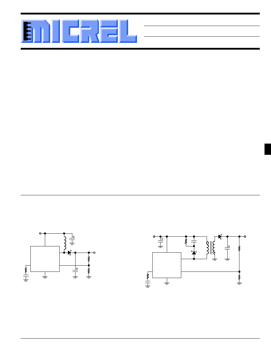
Typical Applications
C4
470µF
D2
1N5818
C1
47µF
C2
1µF
R3
1k
R4*
V
OUT
5V, 0.5A
* Optional voltage clipper (may be req'd if T1 leakage inductance too high)
C3*
D1*
R1
3.74k
1%
R2
1.24k
1%
V
IN
4V to 6V
T1
1:1.25
L
PRI
= 12µH
MIC2171
IN
SW
FB
GND
COMP
Figure 2.
MIC2171 5V Flyback Converter
+5V
(4.75V min.)
D1
1N5822
MIC2171
IN
SW
FB
C1*
47µF
R3
1k
C3
1µF
R1
10.7k
1%
C2
470µF
V
OUT
+12V, 0.25A
L1
15µH
* Locate near MIC2171 when supply leads > 2
"
R2
1.24k
1%
GND
COMP
Figure 1.
MIC2171 5V to 12V Boost Converter

MIC2171
Micrel
4-4
1997
Ordering Information
Part Number
Temperature Range
Package
MIC2171BT
≠40
∞
C to +85
∞
C
5-lead TO-220
MIC2171BU
≠40
∞
C to +85
∞
C
5-lead TO-263
5-lead TO-263 (BU)
5-lead TO-220 (BT)
Tab GND
5 IN
4 SW
3 GND
2 FB
1 COMP
Pin Configuration
Tab GND
5 IN
4 SW
3 GND
2 FB
1 COMP
Pin Description
Pin Number
Pin Name
Pin Function
1
COMP
Frequency Compensation: Output of transconductance-type error amplifier.
Primary function is for loop stabilization. Can also be used for output voltage
soft-start and current limit tailoring.
2
FB
Feedback: Inverting input of error amplifier. Connect to external resistive
divider to set power supply output voltage.
3
GND
Ground: Connect directly to the input filter capacitor for proper operation
(see applications info).
4
SW
Power Switch Collector: Collector of NPN switch. Connect to external
inductor or input voltage depending on circuit topology.
5
IN
Supply Voltage: 3.0V to 40V

1997
4-5
MIC2171
Micrel
4
Electrical Characteristics
V
IN
= 5V; T
A
= 25
∞
C, bold values indicate ≠40
∞
C
T
A
+85
∞
C; unless noted.
Parameter
Conditions
Min
Typ
Max
Units
Reference Section
Feedback Voltage (V
FB
)
V
COMP
= 1.24V
1.220
1.240
1.264
V
1.214
1.274
V
Feedback Voltage
3V
V
IN
40V
.06
%/V
Line Regulation
V
COMP
= 1.24V
Feedback Bias Current (I
FB
)
V
FB
= 1.24V
310
750
nA
1100
nA
Error Amplifier Section
Transconductance (g
m
)
I
COMP
=
±
25
µ
A
3.0
3.9
6.0
µ
A/mV
2.4
7.0
µ
A/mV
Voltage Gain (A
V
)
0.9V
V
COMP
1.4V
400
800
2000
V/V
Output Current
V
COMP
= 1.5V
125
175
350
µ
A
100
400
µ
A
Output Swing
High Clamp, V
FB
= 1V
1.8
2.1
2.3
V
Low Clamp, V
FB
= 1.5V
0.25
0.35
0.52
V
Compensation Pin
Duty Cycle = 0
0.8
0.9
1.08
V
Threshold
0.6
1.25
V
Output Switch Section
ON Resistance
I
SW
= 2A, V
FB
= 0.8V
0.37
0.50
0.55
Current Limit
Duty Cycle = 50%, T
J
25
∞
C
2.5
3.6
5
A
Duty Cycle = 50%, T
J
< 25
∞
C
2.5
4.0
5.5
A
Duty Cycle = 80%, Note 3
2.0
3.0
5
A
Breakdown Voltage (BV)
3V
V
IN
40V
65
75
V
I
SW
= 5mA
Oscillator Section
Frequency (f
O
)
88
100
112
kHz
85
115
kHz
Duty Cycle [
(max)]
80
90
95
%
Input Supply Voltage Section
Minimum Operating Voltage
2.7
3.0
V
Quiescent Current (I
Q
)
3V
V
IN
40V, V
COMP
= 0.6V, I
SW
= 0
7
9
mA
Supply Current Increase (
I
IN
)
I
SW
= 2A, V
COMP
= 1.5V, during swich on-time
9
20
mA
General Note Devices are ESD sensitive. Handling precautions required.
Note 1
Mounted vertically, no external heat sink, 1/4 inch leads soldered to PC board containing approximently 4 inch squared copper area
surrounding leads.
Note 2
All ground leads soldered to approximently 2 inches squared of horizontal PC board copper area.
Note 3
For duty cycles (
) between 50% and 95%, minimum guaranteed switch current is I
CL
= 1.66 (2-
) Amp (Pk).
Absolute Maximum Ratings
Input Voltage (V
IN
) ........................................................ 40V
Switch Voltage (V
SW
) .................................................... 65V
Feedback Voltage (transient, 1ms) (V
FB
) ...................
±
15V
Operating Temperature Range ...................... ≠40 to +85
∞
C
Junction Temperature ................................ ≠55
∞
C to 150
∞
C
Thermal Resistance
JA
5-lead TO-220, Note 1 ................................. 45
∞
C/W
JA
5-lead TO-263, Note 2 ................................. 45
∞
C/W
Storage Temperature ............................... ≠65
∞
C to +150
∞
C
Soldering (10 sec.) .................................................. +300
∞
C
MIC2171
Micrel
4-6
1997
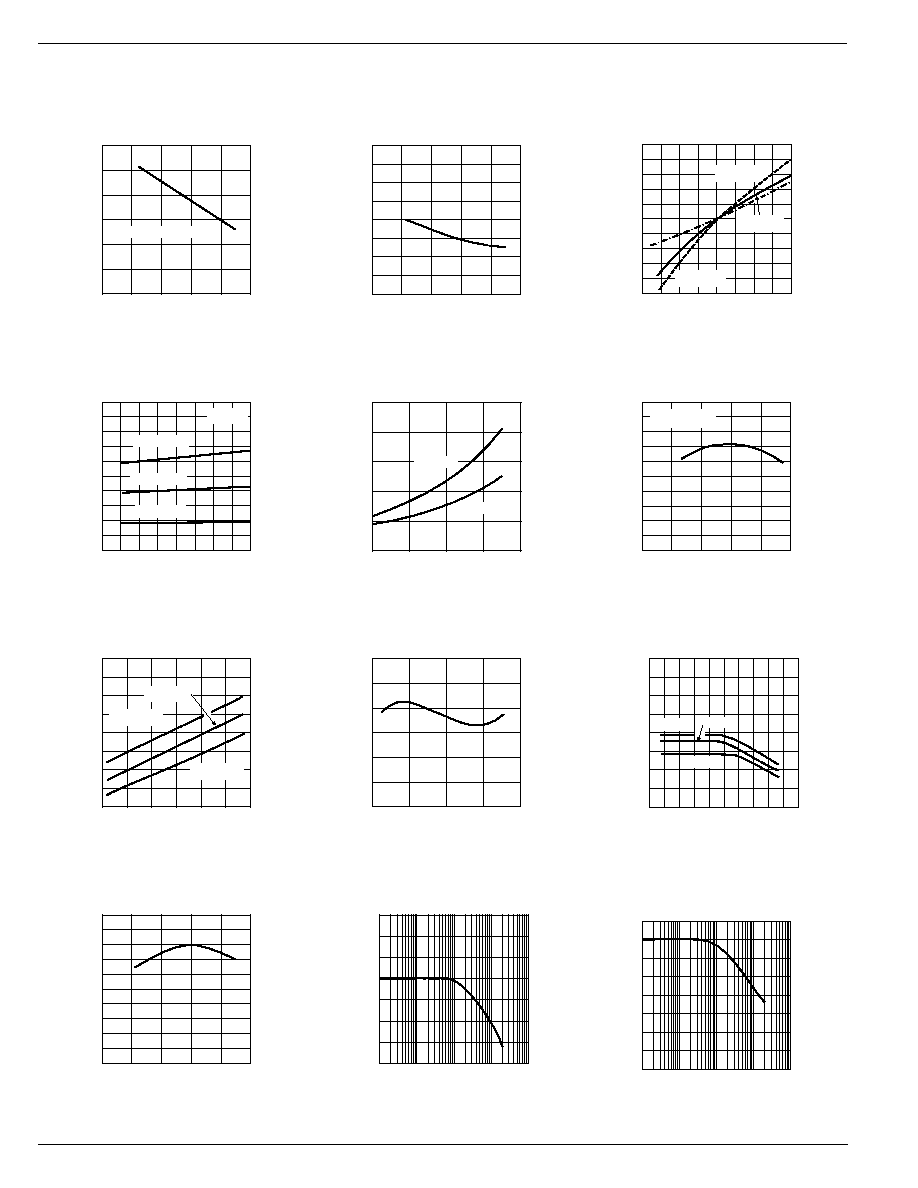
2.3
2.4
2.5
2.6
2.7
2.8
2.9
-100
-50
0
50
100
150
Minimum Operating Voltage (V)
Temperature (
∞
C)
Minimum
Operating Voltage
Switch Current = 2A
0
100
200
300
400
500
600
700
800
-100
-50
0
50
100
150
Feedback Bias Current (nA)
Temperature (
∞
C)
Feedback Bias Current
-5
-4
-3
-2
-1
0
1
2
3
4
5
0
10
20
30
40
Feedback Voltage Change (mV)
V
IN
Operating (V)
Feedback Voltage
Line Regulation
T
J
= -40
∞
C
T
J
= 25
∞
C
T
J
= 125
∞
C
5
6
7
8
9
10
11
12
13
14
15
0
10
20
30
40
Supply Current (mA)
V
IN
Operating Voltage (V)
Supply Current
I
SW
= 0
D.C. = 90%
D.C. = 50%
D.C. = 0%
0
0.2
0.4
0.6
0.8
1.0
1.2
1.4
1.6
0
1
2
3
Switch ON Voltage (V)
Switch Current (A)
Switch On-Voltage
T
J
= 25
∞
C
T
J
= 125
∞
C
T
J
= ≠40
∞
C
60
70
80
90
100
110
120
-50
0
50
100
150
Frequency (kHz)
Temperature (
∞
C)
Oscillator Frequency
0
2
4
6
8
0
20
40
60
80
100
Switch Current (A)
Duty Cycle (%)
Current Limit
≠40
∞
C
25
∞
C
125
∞
C
Error Amplifier Gain
0.0
0.5
1.0
1.5
2.0
2.5
3.0
3.5
4.0
4.5
5.0
-100
-50
0
50
100
150
Transconductance (
µ
A/mV)
Temperature (
∞
C)
0
1000
2000
3000
4000
5000
6000
7000
1
10
100
1000
10000
Transconductance (
µ
S)
Frequency (kHz)
Error Amplifier Gain
210
180
150
120
90
60
30
0
-30
1
10
100
1000
10000
Phase Shift (
∞
)
Frequency (kHz)
Error Amplifier Phase
Typical Performance Characteristics
0
10
20
30
40
50
0
1
2
3
4
Average Supply Current (mA)
Switch Current (A)
Supply Current
= 90%
= 50%
0
1
2
3
4
5
6
7
8
9
10
-100
-50
0
50
100
150
Supply Current (mA)
Temperature (
∞
C)
Supply Current
V
COMP
= 0.6V
1997
4-7
MIC2171
Micrel
4
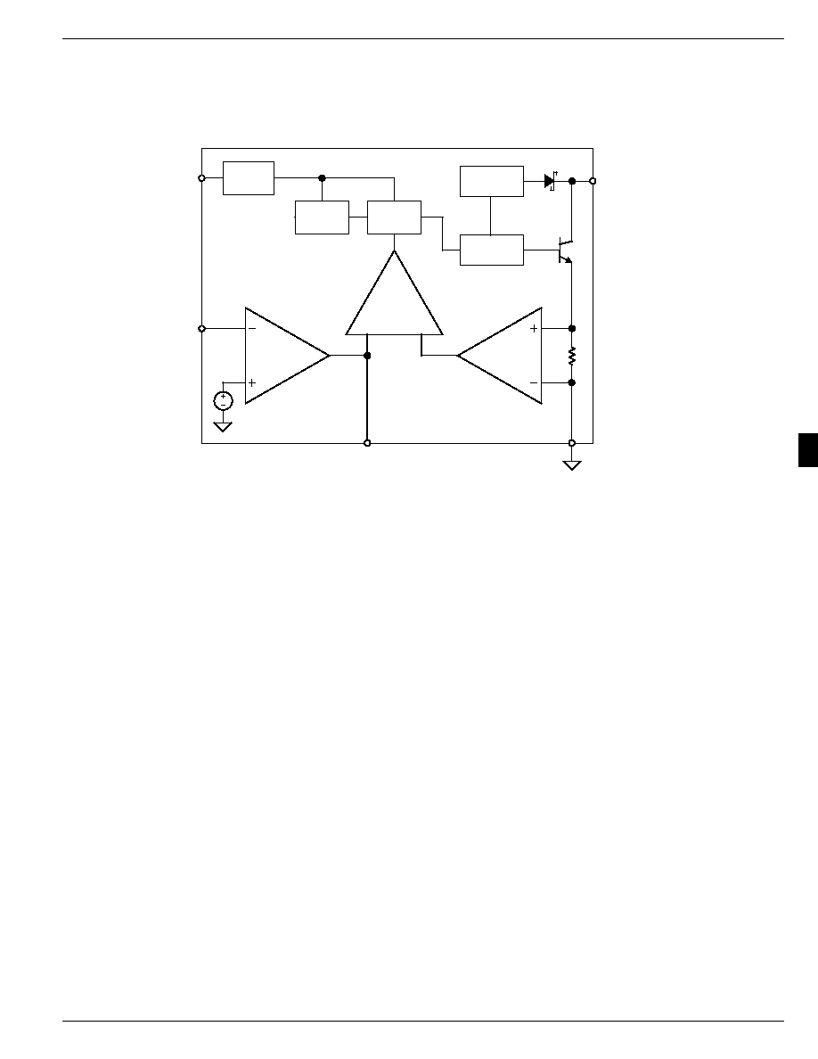
Block Diagram MIC2171
Current
Amp.
Error
Amp.
1.24V
Ref.
Logic
Driver
Anti-Sat.
SW
100kHz
Osc.
Reg.
FB
COMP
GND
IN
D1
Q1
2.3V
Com-
parator
Functional Description
Refer to "Block Diagram MIC2171".
Internal Power
The MIC2171 operates when V
IN
is
2.6V. An internal 2.3V
regulator supplies biasing to all internal circuitry including a
precision 1.24V band gap reference.
PWM Operation
The 100kHz oscillator generates a signal with a duty cycle of
approximately 90%. The current-mode comparator output is
used to reduce the duty cycle when the current amplifier
output voltage exceeds the error amplifier output voltage.
The resulting PWM signal controls a driver which supplies
base current to output transistor Q1.
Current-Mode Advantages
The MIC2171 operates in current mode rather than voltage
mode. There are three distinct advantages to this technique.
Feedback loop compensation is greatly simplified because
inductor current sensing removes a pole from the closed loop
response. Inherent cycle-by-cycle current limiting greatly
improves the power switch reliability and provides automatic
output current limiting. Finally, current-mode operation pro-
vides automatic input voltage feed forward which prevents
instantaneous input voltage changes from disturbing the
output voltage setting.
Anti-Saturation
The anti-saturation diode (D1) increases the usable duty
cycle range of the MIC2171 by eliminating the base to
collector stored charge which would delay Q1's turnoff.
Compensation
Loop stability compensation of the MIC2171 can be accom-
plished by connecting an appropriate network from either
COMP to circuit ground (see typical Applications) or COMP
to FB.
The error amplifier output (COMP) is also useful for soft start
and current limiting. Because the error amplifier output is a
transconductance type, the output impedance is relatively
high which means the output voltage can be easily clamped
or adjusted externally.