
1997
1
MIC2172/3172
MIC2172/3172
Micrel
slave's. The master MIC2172's oscillator frequency is in-
creased up to 135kHz by connecting a resistor from SYNC to
ground (see applications information).
The MIC2172/3172 is available in an 8-pin plastic DIP or
SOIC for ≠40
∞
C to +85
∞
C operation.
Features
∑ 1.25A, 65V internal switch rating
∑ 3V to 40V input voltage range
∑ Current-mode operation
∑ Internal cycle-by-cycle current limit
∑ Thermal shutdown
∑ Low external parts count
∑ Operates in most switching topologies
∑ 7mA quiescent current (operating)
∑ <1
µ
A quiescent current, shutdown mode (MIC3172)
∑ TTL shutdown compatibility (MIC3172)
∑ External frequency synchronization (MIC2172)
∑ External frequency trim (MIC2172)
∑ Fits most LT1172 sockets (see applications info)
Applications
∑ Laptop/palmtop computers
∑ Toys
∑ Hand-held instruments
∑ Off-line converter up to 50W
(requires external power switch)
∑ Predriver for higher power capability
∑ Master/slave configurations (MIC2172)
General Description
The MIC2172 and MIC3172 are complete 100kHz SMPS
current-mode controllers with internal 65V 1.25A power
switches. The MIC2172 features external frequency syn-
chronization or frequency adjustment, while the MIC3172
features an enable/shutdown control input.
Although primarily intended for voltage step-up applications,
the floating switch architecture of the MIC2172/3172 makes
it practical for step-down, inverting, and Cuk configurations
as well as isolated topologies.
Operating from 3V to 40V, the MIC2172/3172 draws only
7mA of quiescent current making it attractive for battery
operated supplies.
The MIC3172 is for applications that require on/off control of
the regulator. The MIC3172 is externally shutdown by
applying a TTL low signal to EN (enable). When disabled, the
MIC3172 draws only leakage current (typically less than
1
µ
A). EN must be high for normal operation. For applications
not requiring control, EN must be tied to V
IN
or TTL high.
The MIC2172 is for applications requiring two or more SMPS
regulators that operate from the same input supply. The
MIC2172 features a SYNC input which allows locking of its
internal oscillator to an external reference. This makes it
possible to avoid the audible beat frequencies that result from
the unequal oscillator frequencies of independent SMPS
regulators.
A reference signal can be supplied by one MIC2172 desig-
nated as a master. To insure locking of the slave's oscillators,
the reference oscillator frequency must be higher than the
MIC2172/3172
100kHz 1.25A Switching Regulators
Final Information
Typical Applications
C4
470µF
D2
1N5818
C1
22µF
C2
1µF
R3
1k
R4*
V
OUT
5V, 0.25A
* Optional voltage clipper (may be req'd if T1 leakage inductance too high)
C3*
D1*
R1
3.74k
1%
R2
1.24k
1%
V
IN
4V to 6V
T1
Enable
Shutdown
1:1.25
L
PRI
= 100µH
MIC3172
V
IN
V
SW
FB
EN
GND
P1 P2 S
COMP
Figure 2.
MIC3172 5V Flyback Converter
+5V
(4.75V min.)
D1
1N5822
MIC2172
V
IN
V
SW
FB
C1*
22µF
R3
1k
C3
1µF
R1
10.7k
1%
C2
470µF
V
OUT
+12V, 0.14A
L1
27µH
* Locate near MIC2172 when supply leads > 2"
R2
1.24k
1%
SYNC
GND
P1 P2 S
N/C
COMP
Figure 1.
MIC2172 5V to 12V Boost Converter
Micrel, Inc. ∑ 1849 Fortune Drive ∑ San Jose, CA 95131 ∑ USA ∑ tel + 1 (408) 944-0800 ∑ fax + 1 (408) 944-0970 ∑ http://www.micrel.com

MIC2172/3172
Micrel
MIC2172/3172
2
1997
Ordering Information
Part Number
Temperature Range
Package
MIC2172BN
≠40
∞
C to +85
∞
C
8-pin plastic DIP
MIC2172BM
≠40
∞
C to +85
∞
C
8-lead SOIC
MIC3172BN
≠40
∞
C to +85
∞
C
8-pin plastic DIP
MIC3172BM
≠40
∞
C to +85
∞
C
8-lead SOIC
8-lead SOIC (M)
1
2
3
4
S GND
COMP
P GND 1
FB
*SYNC/
EN
V
SW
V
I N
P GND 2
8
7
6
5
MIC2172*/3172
Pin Configuration
1
2
3
4
S GND
COMP
P GND 1
FB
*SYNC/
EN
V
SW
V
I N
P GND 2
8
7
6
5
MIC2172*/3172
Pin Description
Pin Number
Pin Name
Pin Function
1
S GND
Signal Ground: Internal analog circuit ground. Connect directly to the input
filter capacitor for proper operation (see applications info). Keep separate
from power grounds.
2
COMP
Frequency Compensation: Output of transconductance type error amplifier.
Primary function is for loop stabilization. Can also be used for output voltage
soft-start and current limit tailoring.
3
FB
Feedback: Inverting input of error amplifier. Connect to external resistive
divider to set power supply output voltage.
4 (MIC2172)
SYNC
Synchronization/Frequency Adjust: Capacitively coupled input signal greater
than device's free running frequency (up to 135kHz) will lock device's
oscillator on falling edge. Oscillator frequency can be trimmed up to 135kHz
by adding a resistor to ground. If unused, pin must float (no connection).
4 (MIC3172)
EN
Enable: Apply TTL high or connect to V
IN
to enable the regulator. Apply
TTL low or connect to ground to disable the regulator. Device draws only
leakage current (<1
µ
A) when disabled.
5
V
IN
Supply Voltage: 3.0V to 40V
6
P GND 2
Power Ground #2: One of two NPN power switch emitters with 0.3
current
sense resistor in series. Required. Connect to external inductor or input
voltage ground depending on circuit topology.
7
V
SW
Power Switch Collector: Collector of NPN switch. Connect to external
inductor or input voltage depending on circuit topology.
8
P GND 1
Power Ground #1: One of two NPN power switch emitters with 0.3
current
sense resistor in series. Optional. For maximum power capability connect
to P GND 2. Floating pin reduces current limit by a factor of two.
8-pin DIP (N)

1997
3
MIC2172/3172
MIC2172/3172
Micrel
Electrical Characteristics MIC2172
Note 1, 3. Unless otherwise specified, V
IN
= 5V.
Parameter
Conditions
Min
Typ
Max
Units
Reference Section
Pin 2 tied to pin 3
Feedback Voltage (V
FB
)
1.220
1.240
1.264
V
1.214
1.274
V
Feedback Voltage
3V
V
IN
40V
0.03
%/V
Line Regulation
Feedback Bias Current (I
FB
)
310
750
nA
1100
nA
Error Amplifier Section
Transconductance (
I
COMP
/
V
FB
)
I
COMP
=
±
25
µ
A
3.0
3.9
6.0
µ
A/mV
2.4
7.0
µ
A/mV
Voltage Gain (
V
COMP
/
V
FB
)
0.9V
V
COMP
1.4V
500
800
2000
V/V
Output Current
V
COMP
= 1.5V
125
175
350
µ
A
100
400
µ
A
Output Swing
High Clamp, V
FB
= 1V
1.8
2.1
2.3
V
Low Clamp, V
FB
= 1.5V
0.25
0.35
0.52
V
Compensation Pin
Duty Cycle = 0
0.8
0.9
1.08
V
Threshold
0.6
1.25
V
Output Switch Section
ON Resistance
I
SW
= 1A, V
FB
= 0.8V
0.76
1
1.1
Current Limit
Duty Cycle = 50%, T
J
25
∞
C
1.25
3
A
Duty Cycle = 50%, T
J
< 25
∞
C
1.25
3.5
A
Duty Cycle = 80% Note 2
1
2.5
A
Breakdown Voltage (BV)
3V
V
IN
40V
65
75
V
I
SW
= 5mA
Absolute Maximum Ratings MIC2172
Input Voltage ................................................................. 40V
Switch Voltage .............................................................. 65V
Sync Current .............................................................. 50mA
Feedback Voltage (Transient, 1ms) ...........................
±
15V
Operating Temperature Range
8-pin PDIP ................................................. ≠40 to +85
∞
C
8-pin SOIC ................................................ ≠40 to +85
∞
C
Junction Temperature .............................. ≠55
∞
C to +150
∞
C
Thermal Resistance
JA
8-pin PDIP ................................................. 130
∞
C/W
JA
8-pin SOIC ................................................. 120
∞
C/W
Storage Temperature ............................... ≠65
∞
C to +150
∞
C
Soldering (10 sec.) .................................................. +300
∞
C

MIC2172/3172
Micrel
MIC2172/3172
4
1997
Parameter
Conditions
Min
Typ
Max
Units
Oscillator Section
Frequency (f
O
)
88
100
112
kHz
85
115
kHz
Duty Cycle [
(max)]
80
89
95
%
Sync Coupling Capacitor
V
PP
= 3.0V
22
51
120
pF
Required for Frequency Lock
V
PP
= 40V
2.2
4.7
10
pF
Peak-to-Peak Voltage
C
COUPLING
= 12pF
2.2
12
30
V
Required for Frequency Lock
Input Supply Voltage Section
Minimum Operating Voltage
2.7
3.0
V
Quiescent Current (I
Q
)
3V
V
IN
40V, V
COMP
= 0.6V, I
SW
= 0
7
9
mA
Supply Current Increase (
I
IN
)
I
SW
= 1A, V
COMP
= 1.5V
9
20
mA
Bold type denotes specifications applicable to the full operating temperature range.
Note 1
Devices are ESD sensitive. Handling precautions required.
Note 2
For duty cycles (
) between 50% and 95%, minimum guaranteed switch current is given by I
CL
= 0.833 (2-
) for the MIC3172.
Note 3
Specification for packaged product only.
Absolute Maximum Ratings MIC3172
Input Voltage ................................................................. 40V
Switch Voltage .............................................................. 65V
Enable Voltage .............................................................. 40V
Feedback Voltage (Transient, 1ms) ...........................
±
15V
Operating Temperature Range
8-pin PDIP ................................................. ≠40 to +85
∞
C
8-pin SOIC ................................................ ≠40 to +85
∞
C
8-pin CerDIP ........................................... ≠55 to +125
∞
C
Junction Temperature ................................ ≠55
∞
C to 150
∞
C
Thermal Resistance
JA
8-pin PDIP ................................................. 130
∞
C/W
JA
8-pin SOIC ................................................. 120
∞
C/W
JA
8-pin CerDIP .............................................. 100
∞
C/W
Storage Temperature ................................. ≠65
∞
C to 150
∞
C
Soldering (10 sec.) .................................................... 300
∞
C
Electrical Characteristics MIC3172
Note 1, 3. Unless otherwise specified, V
IN
= 5V.
Parameter
Conditions
Min
Typ
Max
Units
Reference Section
Pin 2 tied to pin 3
Feedback Voltage (V
FB
)
1.224
1.240
1.264
V
1.214
1.274
V
Feedback Voltage
3V
V
IN
40V
0.07
%/V
Line Regulation
Feedback Bias Current (I
FB
)
310
750
nA
1100
nA

1997
5
MIC2172/3172
MIC2172/3172
Micrel
Parameter
Conditions
Min
Typ
Max
Units
Error Amplifier Section
Transconductance (
I
COMP
/
V
FB
)
I
COMP
=
±
25
µ
A
3.0
3.9
6.0
µ
A/mV
2.4
7.0
µ
A/mV
Voltage Gain (
V
COMP
/
V
FB
)
0.9V
V
COMP
1.4V
500
800
2000
V/V
Output Current
V
COMP
= 1.5V
125
175
350
µ
A
100
400
µ
A
Output Swing
High Clamp, V
FB
= 1V
1.8
2.1
2.3
V
Low Clamp, V
FB
= 1.5V
0.25
0.35
0.52
V
Compensation Pin
Duty Cycle = 0
0.8
0.9
1.08
V
Threshold
0.6
1.25
V
Output Switch Section
ON Resistance
I
SW
= 1A, V
FB
= 0.8V
0.76
1
1.1
Current Limit
Duty Cycle = 50%, T
J
25
∞
C
1.25
3
A
Duty Cycle = 50%, T
J
< 25
∞
C
1.25
3.5
A
Duty Cycle = 80% Note 2
1
2.5
A
Breakdown Voltage (BV)
3V
V
IN
40V
65
75
V
I
SW
= 5mA
Oscillator Section
Frequency (f
O
)
88
100
112
kHz
85
115
kHz
Duty Cycle [
(max)]
80
89
95
%
Input Supply Voltage Section and Enable Section
Minimum Operating Voltage
2.7
3.0
V
Quiescent Current (I
Q
)
3V
V
IN
40V, V
COMP
= 0.6V, I
SW
= 0
7
9
mA
Shutdown, V
EN
= 0V
0.1
5
µ
A
Quiescent Current Increase (
I
IN
)
I
SW
= 1A, V
COMP
= 1.5V
9
20
mA
Enable Input Threshold
0.4
1.2
2.4
V
Enable Input Current
V
EN
= 0V
≠1
0
1
µ
A
V
EN
= 2.4V
2
10
µ
A
Bold type denotes specifications applicable to the full operating temperature range.
Note 1
Devices are ESD sensitive. Handling precautions required.
Note 2
For duty cycles (
) between 50% and 95%, minimum guaranteed switch current is given by I
CL
= 0.833 (2-
) for the MIC3172.
Note 3
Specification for packaged product only.
MIC2172/3172
Micrel
MIC2172/3172
6
1997
2.3
2.4
2.5
2.6
2.7
2.8
2.9
-100
-50
0
50
100
150
Minimum Operating Voltage (V)
Temperature (
∞
C)
MIC2172 Minimum
Operating Voltage
Switch Current = 1A
0
100
200
300
400
500
600
700
800
-100
-50
0
50
100
150
Feedback Bias Current (nA)
Temperature (
∞
C)
Feedback Bias Current
-5
-4
-3
-2
-1
0
1
2
3
4
5
0
10
20
30
40
Feedback Voltage Change (mV)
V
IN
Operating (V)
Feedback Voltage
Line Regulation
T
J
= -40
∞
C
T
J
= 25
∞
C
T
J
= 125
∞
C
5
6
7
8
9
10
11
12
13
14
15
0
10
20
30
40
Supply Current (mA)
V
IN
Operating Voltage (V)
Supply Current
I
SW
= 0
D.C. = 90%
D.C. = 50%
D.C. = 0%
0
1
2
3
4
5
6
7
8
-100
-50
0
50
100
150
Supply Current (
µ
A)
Temperature (
∞
C)
Supply Current
(Shutdown Mode)
MIC3172
V
IN
= 40V
0.8
0.9
1
1.1
1.2
1.3
1.4
-100
-50
0
50
100
150
Enable Pin Voltage (mV)
Temperature (
∞
C)
Enable Thresholds
ON
OFF
MIC3172
0
10
20
30
40
50
0.0
0.5
1.0
1.5
2.0
Average Supply Current (mA)
Switch Current (A)
Supply Current
= 90%
= 50%
0.0
0.2
0.4
0.6
0.8
1.0
1.2
1.4
1.6
0.0
0.5
1.0
1.5
Switch ON Voltage (V)
Switch Current (A)
Switch ON Voltage
T
J
= 25
∞
C
T
J
= 125
∞
C
T
J
= ≠40
∞
C
0
1
2
3
4
0
20
40
60
80
100
Switch Current (A)
Duty Cycle (%)
Current Limit
≠40
∞
C
25
∞
C
125
∞
C
0
1
2
3
4
5
6
7
8
9
10
-100
-50
0
50
100
150
Supply Current (mA)
Temperature (
∞
C)
Supply Current
V
COMP
= 0.6V
60
70
80
90
100
110
120
-50
0
50
100
150
Frequency (kHz)
Temperature (
∞
C)
Oscillator Frequency
90
100
110
120
130
140
1
10
100
1000
f
OSC
(kHz)
R
ADJ
(k
)
Oscillator Frequency
MIC2172
Typical Performance Characteristics
1997
7
MIC2172/3172
MIC2172/3172
Micrel
210
180
150
120
90
60
30
0
-30
1
10
100
1000
10000
Phase Shift (
∞
)
Frequency (kHz)
Error Amplifier Phase
Typical Performance Characteristics
0
1000
2000
3000
4000
5000
6000
7000
1
10
100
1000
10000
Transconductance (
µ
S)
Frequency (kHz)
Error Amplifier Gain
Error Amplifier Gain
0.0
0.5
1.0
1.5
2.0
2.5
3.0
3.5
4.0
4.5
5.0
-100
-50
0
50
100
150
Transconductance (
µ
A/mV)
Temperature (
∞
C)
Block Diagram MIC2172
Current
Amp.
Error
Amp.
1.24V
Ref.
Logic
Driver
Anti-Sat.
V
SW
Pin 7
100kHz
Osc.
SYNC
Pin 4
Reg.
FB
Pin 3
COMP
Pin 2
P
GND
2
Pin 6
P
GND
1
Pin 8
V
I N
P i n 5
S
GND
Pin 1
D1
Q1
2.3V
Com-
parator
MIC2172/3172
Micrel
MIC2172/3172
8
1997
Functional Description
Refer to "Block Diagram MIC2172" and "Block Diagram
MIC3172."
Internal Power
The MIC2172/3172 operates when V
IN
is
2.6V (and V
EN
2.0V for the MIC3172). An internal 2.3V regulator supplies
biasing to all internal circuitry including a precision 1.24V
band gap reference.
The enable control (MIC3172 only) enables or disables the
internal regulator which supplies power to all other internal
circuitry.
PWM Operation
The 100kHz oscillator generates a signal with a duty cycle of
approximately 90%. The current-mode comparator output is
used to reduce the duty cycle when the current amplifier
output voltage exceeds the error amplifier output voltage.
The resulting PWM signal controls a driver which supplies
base current to output transistor Q1.
Current Mode Advantages
The MIC2172/3172 operates in current mode rather than
voltage mode. There are three distinct advantages to this
technique. Feedback loop compensation is greatly simplified
because inductor current sensing removes a pole from the
closed loop response. Inherent cycle-by-cycle current limit-
ing greatly improves the power switch reliability and provides
automatic output current limiting. Finally, current-mode op-
eration provides automatic input voltage feed forward which
prevents instantaneous input voltage changes from disturb-
ing the output voltage setting.
Anti-Saturation
The anti-saturation diode (D1) increases the usable duty
cycle range of the MIC2172/3172 by eliminating the base to
collector stored charge which would delay Q1's turnoff.
Compensation
Loop stability compensation of the MIC2172/3172 can be
accomplished by connecting an appropriate network from
either COMP to circuit ground (Typical Applications) or COMP
to FB.
The error amplifier output (COMP) is also useful for soft start
and current limiting. Because the error amplifier output is a
transconductance type, the output impedance is relatively
high which means the output voltage can be easily clamped
or adjusted externally.
Block Diagram MIC3172
Current
Amp.
Error
Amp.
1.24V
Ref.
Logic
Driver
Anti-Sat.
V
SW
Pin 7
100kHz
Osc.
EN
Pin 4
Reg.
FB
Pin 3
COMP
Pin 2
P
GND
2
Pin 6
P
GND
1
Pin 8
V
I N
P i n 5
S
GND
Pin 1
D1
Q1
2.3V
Com-
parator
1997
9
MIC2172/3172
MIC2172/3172
Micrel
By using the MIC3172, U1 and Q1 shown in figure 5 can be
eliminated, reducing the total components count.
Synchronizing the MIC2172
Using several unsynchronized switching regulators in the
same circuit will cause beat frequencies to appear on the
inputs and outputs. These beat frequencies can be very low
making them difficult to filter.
Micrel's MIC2172 can be synchronized to a single master
frequency avoiding the possibility of undesirable beat fre-
quencies in multiple regulator circuits. The master frequency
can be an external oscillator or a designated master MIC2172.
The master frequency should be 1.05 to 1.20 times the
slave's 100kHz nominal frequency to guarantee synchroni-
zation.
4
5
Additional
Slaves
Master
10k
U3
MIC2172
V
SW
SYNC
4
5
Slave
U2
MIC2172
V
SW
SYNC
U1
4
5
Slave
MIC2172
V
SW
SYNC
Figure 6. Master/Slave Synchronization
Figure 6 shows a typical application where several MIC2172s
operate from the same supply voltage. U1's oscillator fre-
quency is increased above U2's and U3's by connecting a
resistor from SYNC to ground. U2-SYNC and U3-SYNC are
capacitively coupled to the master's output (V
SW
). The
slaves lock to the negative (falling edge) of U1's output
waveform.
Additional
Slaves
U2
4
5
Slave
U1
MIC2172
V
SW
SYNC
4
5
Slave
MIC2172
V
SW
SYNC
External
Signal
Figure 7. External Synchronization
Care must be exercised to insure that the master MIC2172 is
always operating in continuous mode.
Applications Information
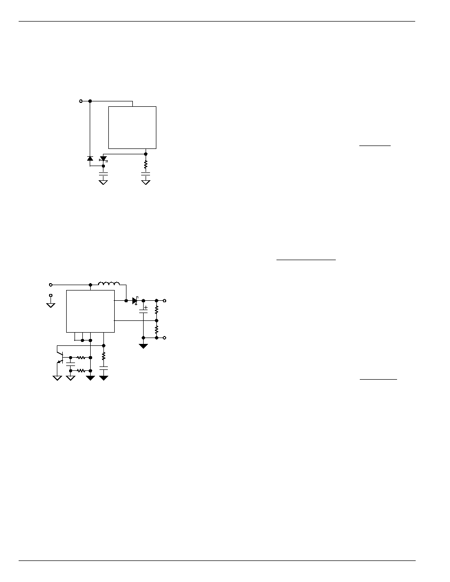
Using the MIC3172 Enable Control (New Designs)
For new designs requiring enable/shutdown control, connect
EN to a TTL or CMOS control signal (figure 3). The very low
driver current requirement ensures compatibility regardless
of the driver or gate used.
MIC3172
EN
Enable
Shutdown
U1
Logic
Gate
4
Figure 3. MIC3172 TTL Enable/Shutdown
Using the MIC3172 in LT1172 Applications
The MIC3172 can be used in most original LT1172 applica-
tions by adapting the MIC3172's enable/shutdown feature to
the existing LT1172 circuit.
Unlike the LT1172 which can be shutdown by reducing the
voltage on pin 2 (V
C
) below 0.15V, the MIC3172 has a
dedicated enable/shutdown pin. To replace the LT1172 with
the MIC3172, determine if the LT1172's shutdown feature is
used.
Circuits without Shutdown
If the shutdown feature is not being used, connect EN to V
IN
to continuously enable the MIC3172 or use an MIC2172 with
SYNC open (figure 4).
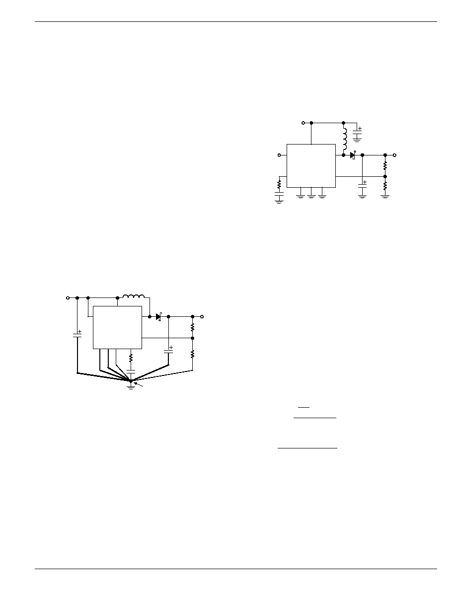
MIC2172
V
IN
V
IN
SYNC
4
MIC3172
V
IN
V
IN
EN
4
N/C
Figure 4. MIC2172/3172 Always Enabled
Circuits with Shutdown
If shutdown was used in the original LT1172 application,
connect EN to a logic gate that produces a TTL logic-level
output signal that matches the shutdown signal. The MIC3172
will be enabled by a logic-high input and shutdown with a
logic-low input (figure 5). The actual components performing
the functions of U1 and Q1 may vary according to the original
application.
MIC3172
COMP
C1
R1
EN
Existing
Q1
VN2222
or equiv.
U1
Existing
Logic
Gate
add
connection
4
Enable
Shutdown
Figure 5. Adapting to the LT1172 Socket
MIC2172/3172
Micrel
MIC2172/3172
10
1997
Figure 7 shows how one or more MIC2172s can be locked to
an external reference frequency. The slaves lock to the
negative (falling edge) of the external reference waveform.
Soft Start
A diode-coupled capacitor from COMP to circuit ground
slows the output voltage rise at turn on (figure 8).
MIC2172/3172
V
IN
COMP
C2
R1
V
IN
D2
C1
D1
Figure 8. Soft Start
The additional time it takes for the error amplifier to charge the
capacitor corresponds to the time it takes the output to reach
regulation. Diode D1 discharges C1 when V
IN
is removed.
Current Limit
For designs demanding less output current than the MIC2172/
3172 is capable of delivering, P GND 1 can be left open
reducing the current capability of Q1 by one-half.
MIC2172/3172
V
IN
COMP
C2
R3
V
IN
Q1
R2
GND
P1 P2 S
R1
C1
V
SW
FB
V
OUT
Note: Input and output
returns not common.
I
CL
0.6V/R2
Figure 9. Current Limit
Alternatively, the maximum current limit of the MIC2172/3172
can be reduced by adding a voltage clamp to the COMP
output (figure 9). This feature can be useful in applications
requiring either a complete shutdown of Q1's switching action
or a form of current fold-back limiting. This use of the COMP
output does not disable the oscillator, amplifiers or other
circuitry, therefore the supply current is never less than
approximately 5mA.
Thermal Management
Although the MIC2172/3172 family contains thermal protec-
tion circuitry, for best reliability, avoid prolonged operation
with junction temperatures near the rated maximum.
The junction temperature is determined by first calculating
the power dissipation of the device. For the MIC2172/3172,
the total power dissipation is the sum of the device operating
losses and power switch losses.
The device operating losses are the dc losses associated
with biasing all of the internal functions plus the losses of the
power switch driver circuitry. The dc losses are calculated
from the supply voltage (V
IN
) and device supply current (I
Q
).
The MIC2172/3172 supply current is almost constant regard-
less of the supply voltage (see "Electrical Characteristics").
The driver section losses (not including the switch) are a
function of supply voltage, power switch current, and duty
cycle.
P
(bias+driver)
= V
IN
I
Q
(
)
+
V
IN
I
SW
0.004 +
50
where:
P
(bias+driver)
= device operating losses
V
IN
= supply voltage
I
Q
= quiescent supply current
I
SW
= power switch current
(see " Design Hints: Switch Current
Calculations")
= duty cycle
=
V
OUT
+ V
F
≠ V
IN
V
OUT
+ V
F
V
OUT
= output voltage
V
F
= D1 forward voltage drop
As a practical example refer to figure 1.
V
IN
= 5.0V
I
Q
= 0.006A
I
SW
= 0.625A
= 60% (0.6)
Then:
P
(bias+driver)
= 5
◊
0.006
(
)
+
5 0.625
0.004 + 0.6
50
P
(bias+driver)
= 0.068W
Power switch dissipation calculations are greatly simplified
by making two assumptions which are usually fairly accurate.
First, the majority of losses in the power switch are due to
on-losses. To find these losses, assign a resistance value to
the collector/emitter terminals of the device using the satura-
tion voltage versus collector current curves (see Typical
Performance Characteristics). Power switch losses are
calculated by modeling the switch as a resistor with the switch
duty cycle modifying the average power dissipation.
P
SW
= (I
SW
)
2
R
SW
From the Typical performance Characteristics:
R
SW
= 1
1997
11
MIC2172/3172
MIC2172/3172
Micrel
Then:
P
SW
= (0.625)
2
◊
1
◊
0.6
P
(SW)
= 0.234W
P
(total)
= 0.068 + 0.234
P
(total)
= 0.302W
The junction temperature for any semiconductor is calculated
using the following:
T
J
= T
A
+ P
(total)
JA
Where:
T
J
= junction temperature
T
A
= ambient temperature (maximum)
P
(total)
= total power dissipation
JA
= junction to ambient thermal resistance
For the practical example:
T
A
= 70
∞
C
JA
= 130
∞
C/W (for plastic DIP)
Then:
T
J
= 70 + 0.30
◊
130
T
J
= 109
∞
C
This junction temperature is below the rated maximum of
150
∞
C.
Grounding
Refer to figure 10. Heavy lines indicate high current paths.
MIC2172/3172
V
IN
V
SW
FB
V
C
V
IN
* MIC3172 only
EN
*
GND
P1 P2 S
Single point ground
Figure 10. Single Point Ground
A single point ground is strongly recommended for proper
operation.
The signal ground, compensation network ground, and feed-
back network connections are sensitive to minor voltage
variations. The input and output capacitor grounds and
power ground conductors will exhibit voltage drop when
carrying large currents. Keep the sensitive circuit ground
traces separate from the power ground traces. Small voltage
variations applied to the sensitive circuits can prevent the
MIC2172/3172 or any switching regulator from functioning
properly.
Applications and Design Hints
Access to both the collector and emitter(s) of the NPN power
switch makes the MIC2172/3172 extremely versatile and
suitable for use in most PWM power supply topologies.
Boost Conversion
Refer to figure 11 for a typical boost conversion application
where a +5V logic supply is available but +12V at 0.14A is
required.
+5V
(4.75V min.)
D1
1N5822
MIC2172
V
IN
V
SW
FB
C1*
22µF
R3
1k
C3
1µF
R1
10.7k
1%
C2
470µF
V
OUT
+12V, 0.14A
L1
27µH
* Locate near MIC2172 when supply leads > 2"
R2
1.24k
1%
SYNC
GND
P1 P2 S
N/C
COMP
Figure 11. 5V to 12V Boost Converter
The first step in designing a boost converter is determining
whether inductor L1 will cause the converter to operate in
either continuous or discontinuous mode. Discontinuous
mode is preferred because the feedback control of the
converter is simpler.
When L1 discharges its current completely during the
MIC2172/3172's off-time, it is operating in discontinuous
mode.
L1 is operating in continuous mode if it does not discharge
completely before the MIC2172/3172 power switch is turned
on again.
Discontinuous Mode Design
Given the maximum output current, solve equation (1) to
determine whether the device can operate in discontinuous
mode without initiating the internal device current limit.
(1)
I
OUT
I
CL
2
V
IN
V
OUT
(1a)
=
V
OUT
+ V
F
≠ V
IN
V
OUT
+ V
F
Where:
I
CL
= internal switch current limit
I
CL
= 1.25A when
< 50%
I
CL
= 0.833 (2 ≠
) when
50%
(Refer to Electrical Characteristics.)
I
OUT
= maximum output current
V
IN
= minimum input voltage
= duty cycle

MIC2172/3172
Micrel
MIC2172/3172
12
1997
V
OUT
= required output voltage
V
F
= D1 forward voltage drop
For the example in figure 11.
I
OUT
= 0.14A
I
CL
= 1.147A
V
IN
= 4.75V (minimum)
= 0.623
V
OUT
= 12.0V
V
F
= 0.6V
Then:
I
OUT
1.147
2
◊
4.75
◊
0.623
12
I
OUT
0.141A
This value is greater than the 0.14A output current require-
ment so we can proceed to find the inductance value of L1.
(2)
L1
V
IN
(
)
2
2 P
OUT
f
SW
Where:
P
OUT
= 12
◊
0.14 = 1.68W
f
SW
= 1
◊
10
5
Hz (100kHz)
For our practical example:
L1
4.75
◊
0.623
(
)
2
2
◊
1.68
◊
1
◊
10
5
I
L1
26.062
µ
H (use 27
µ
H)
Equation (3) solves for L1's maximum current value.
(3)
I
L1(peak)
=
V
IN
T
ON
L1
Where:
T
ON
=
/ f
SW
= 6.23
◊
10
-6
sec
I
L1(peak)
=
4.75
◊
6.23
◊
10
-6
27
◊
10
-6
I
L1(peak)
= 1.096A
Use a 27
µ
H inductor with a peak current rating of at least
1.4A.
Flyback Conversion
Flyback converter topology may be used in low power appli-
cations where voltage isolation is required or whenever the
input voltage can be less than or greater than the output
voltage. As with the step-up converter the inductor (trans-
former primary) current can be continuous or discontinuous.
Discontinuous operation is recommended.
Figure 12 shows a practical flyback converter design using
the MIC3172.
Switch Operation
During Q1's on time (Q1 is the internal NPN transistor--see
block diagrams), energy is stored in T1's primary inductance.
During Q1's off time, stored energy is partially discharged into
C4 (output filter capacitor). Careful selection of a low ESR
capacitor for C4 may provide satisfactory output ripple volt-
age making additional filter stages unnecessary.
C1 (input capacitor) may be reduced or eliminated if the
MIC3172 is located near a low impedance voltage source.
Output Diode
The output diode allows T1 to store energy in its primary
inductance (D2 nonconducting) and release energy into C4
(D2 conducting). The low forward voltage drop of a Schottky
diode minimizes power loss in D2.
Frequency Compensation
A simple frequency compensation network consisting of R3
and C2 prevents output oscillations.
High impedance output stages (transconductance type) in
the MIC2172/3172 often permit simplified loop-stability solu-
tions to be connected to circuit ground, although a more
conventional technique of connecting the components from
the error amplifier output to its inverting input is also possible.
Voltage Clipper
Care must be taken to minimize T1's leakage inductance,
otherwise it may be necessary to incorporate the voltage
clipper consisting of D1, R4, and C3 to avoid second break-
down (failure) of the MIC3172's power NPN Q1.
Enable/Shutdown
The MIC3172 includes the enable/shutdown feature. When
the device is shutdown, total supply current is less than 1
µ
A.
This is ideal for battery applications where portions of a
system are powered only when needed. If this feature is not
required, simply connect EN to V
IN
or to a TTL high voltage.
Discontinuous Mode Design
When designing a discontinuous flyback converter, first de-
termine whether the device can safely handle the peak
primary current demand placed on it by the output power.
Equation (8) finds the maximum duty cycle required for a
given input voltage and output power. If the duty cycle is
greater than 0.8, discontinuous operation cannot be used.
(8)
2 P
OUT
I
CL
V
IN(min)
For a practical example let:
P
OUT
= 5.0V
◊
0.25A = 1.25W
V
IN
= 4.0V to 6.0V
I
CL
= 1.25A when
< 50%
0.833 (2 ≠
) when
50%

1997
13
MIC2172/3172
MIC2172/3172
Micrel
Then:
2
◊
1.25
1.25
◊
4
0.5 (50%) Use 0.55.
The slightly higher duty cycle value is used to overcome
circuit inefficiencies. A few iterations of equation (8) may be
required if the duty cycle is found to be greater than 50%.
Calculate the maximum transformer turns ratio a, or
N
PRI
/N
SEC
, that will guarantee safe operation of the MIC2172/
3172 power switch.
(9)
a
V
CE
F
CE
≠ V
IN(max)
V
SEC
Where:
a = transformer maximum turns ratio
V
CE
= power switch collector to emitter
maximum voltage
F
CE
= safety derating factor (0.8 for most
commercial and industrial applications)
V
IN(max)
= maximum input voltage
V
SEC
= transformer secondary voltage (V
OUT
+ V
F
)
For the practical example:
V
CE
= 65V max. for the MIC2172/3172
F
CE
= 0.8
V
SEC
= 5.6V
Then:
a
65
◊
0.8 ≠ 6.0
5.6
a
8.2143
Next, calculate the maximum primary inductance required to
store the needed output energy with a power switch duty
cycle of 55%.
(10)
L
PRI
0.5 f
SW
V
IN(min)
2
T
ON
2
P
OUT
Where:
L
PRI
= maximum primary inductance
f
SW
= device switching frequency (100kHz)
V
IN(min)
= minimum input voltage
T
ON
= power switch on time
Then:
L
PRI
0.5
◊
1
◊
10
5
◊
4.0
2
5.5
◊
10
-6
(
)
2
1.25
L
PRI
19.23
µ
H
Use an 18
µ
H primary inductance to overcome circuit ineffi-
ciencies.
To complete the design the inductance value of the second-
ary is found which will guarantee that the energy stored in the
transformer during the power switch on time will be com-
pleted discharged into the output during the off-time. This is
necessary when operating in discontinuous-mode.
(11)
L
SEC
0.5 f
SW
V
SEC
2
T
OFF
2
P
OUT
Where:
L
SEC
= maximum secondary inductance
T
OFF
= power switch off time
Then:
L
SEC
0.5
◊
1
◊
10
5
◊
5.6
2
◊
4.5
◊
10
-6
(
)
2
1.25
L
SEC
25.4
µ
H
Figure 12. MIC3172 5V 0.25A Flyback Converter
C4
470µF
D2
1N5818
C1
22µF
C2
1µF
R3
1k
R4*
V
OUT
5V, 0.25A
* Optional voltage clipper (may be req'd if T1 leakage inductance too high)
C3*
D1*
R1
3.74k
1%
R2
1.24k
1%
V
IN
4V to 6V
T1
Enable
Shutdown
1:1.25
L
PRI
= 100µH
MIC3172
V
IN
V
SW
FB
EN
GND
P1 P2 S
COMP

MIC2172/3172
Micrel
MIC2172/3172
14
1997
Finally, recalculate the transformer turns ratio to insure that
it is less than the value earlier found in equation (9).
(12)
a
L
PRI
L
SEC
Then:
a
1.8
◊
10
-5
2.54
◊
10
-5
a
0.84 Use 0.8 (same as 1:1.25).
This ratio is less than the ratio calculated in equation (9).
When specifying the transformer it is necessary to know the
primary peak current which must be withstood without satu-
rating the transformer core.
(13)
I
PEAK(pri)
=
V
IN(min)
T
ON
L
PRI
So:
I
PEAK(pri)
=
4.0
◊
5.5
◊
10
-6
18
µ
H
I
PEAK(pri)
= 1.22A
Now find the minimum reverse voltage requirement for the
output rectifier. This rectifier must have an average current
rating greater than the maximum output current of 0.25A.
(14)
V
BR
V
IN(max)
+ V
OUT
a
(
)
F
BR
a
Where:
V
BR
= output rectifier maximum peak
reverse voltage rating
a = transformer turns ratio (0.8)
F
BR
= reverse voltage safety derating factor (0.8)
Then:
V
BR
6.0 + 5.0
◊
0.8
(
)
0.8
◊
0.8
V
BR
15.625V
A 1N5817 will safely handle voltage and current require-
ments in this example.
Forward Converters
Micrel's MIC2172/3172 can be used in several circuit con-
figurations to generate an output voltage which is less than
the input voltage (buck or step-down topology). Figure 13
shows the MIC3172 in a voltage step-down application.
Because of the internal architecture of these devices, more
external components are required to implement a step-down
regulator than with other devices offered by Micrel (refer to
the LM257x or LM457x family of buck switchers). However,
for step-down conversion requiring a transformer (forward),
the MIC2172/3172 is a good choice.
A 12V to 5V step-down converter using transformer isolation
(forward) is shown in figure 14. Unlike the isolated flyback
converter which stores energy in the primary inductance
during the controller's on-time and releases it to the load
during the off-time, the forward converter transfers energy to
the output during the on-time, using the off-time to reset the
transformer core. In the application shown, the transformer
core is reset by the tertiary winding discharging T1's peak
magnetizing current through D2.
For most forward converters the duty cycle is limited to 50%,
allowing the transformer flux to reset with only two times the
input voltage appearing across the power switch. Although
during normal operation this circuit's duty cycle is well below
C2
2.2µF
C1*
100µF
D2
R4
10
R2
1.2k
C4
1µF
C5
330µF
L1
100µH
R3
3.7k
D1
1N4148
V
IN
D3
1N4148
* Locate near MIC2172/3172 when supply leads > 2"
R3/R2 sets output voltage
5V, 0.1A to 1A
(I
LOAD
> 100mA)
MIC3172
V
IN
V
SW
FB
R3
470
C3
1µF
EN
GND
P1 P2 S
COMP
Figure 13. Step-Down or Buck Converter

1997
15
MIC2172/3172
MIC2172/3172
Micrel
50%, the MIC2172 (and MIC3172) has a maximum duty cycle
capability of 90%. If 90% was required during operation
(start-up and high load currents), a complete reset of the
transformer during the off-time would require the voltage
across the power switch to be ten times the input voltage.
This would limit the input voltage to 6V or less for forward
converter applications.
To prevent core saturation, the application given here uses a
duty cycle limiter consisting of Q1, C4 and R3. Whenever the
MIC3172 exceeds a duty cycle of 50%, T1's reset winding
current turns Q1 on. This action reduces the duty cycle of the
MIC3172 until T1 is able to reset during each cycle.
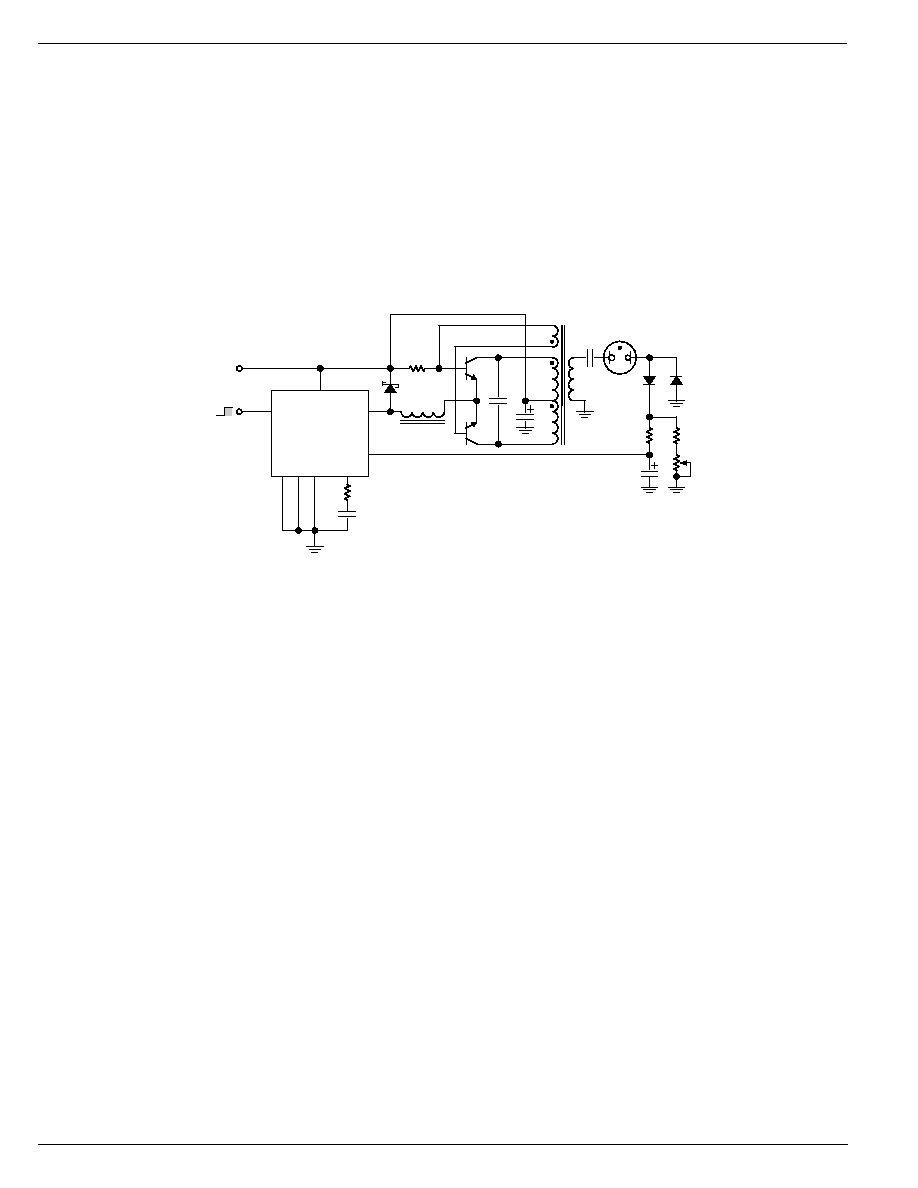
Fluorescent Lamp Supply
An extremely useful application of the MIC3172 is generating
an ac voltage for fluorescent lamps used as liquid crystal
display back lighting in portable computers.
Figure 15 shows a complete power supply for lighting a
fluorescent lamp. Transistors Q1 and Q2 together with ca-
pacitor C2 form a Royer oscillator. The Royer oscillator
generates a sine wave whose frequency is determined by the
series L/C circuit comprised of T1 and C2. Assuming that the
MIC3172 and L1 are absent, and the transistors' emitters are
grounded, circuit operation is described in "Oscillator Opera-
tion."
Oscillator Operation
Resistor R2 provides initial base current that turns transistor
Q1 on and impresses the input voltage across one half of T1's
primary winding (Pri 1). T1's feedback winding provides
additional base drive (positive feedback) to Q1 forcing it well
into saturation for a period determined by the Pri 1/C2 time
constant. Once the voltage across C2 has reached its
maximum circuit value, Q1's collector current will no longer
increase. Since T1 is in series with Q1, this drop in primary
current causes the flux in T1 to change and because of the
mutual coupling to the feedback winding further reduces
primary current eventually turning Q1 off. The primary wind-
ings now change state with the feedback winding forcing Q2
on repeating the alternate half cycle exactly as with Q1. This
action produces a sinusoidal voltage wave form; whose
amplitude is proportional to the input voltage, across T1's
primary winding which is stepped up and capacitively coupled
to the lamp.
Lamp Current Regulation
Initial ionization (lighting) of the fluorescent lamp requires
several times the ac voltage across it than is required to
sustain current through the device. The current through the
lamp is sampled and regulated by the MIC3172 to achieve a
given intensity. The MIC3172 uses L1 to maintain a constant
average current through the transistor emitters. This current
controls the voltage amplitude of the Royer oscillator and
maintains the lamp current. During the negative half cycle,
lamp current is rectified by D3. During the positive half cycle,
lamp current is rectified by D2 through R4 and R5. R3 and C5
filter the voltage dropped across R4 and R5 to the MIC3172's
feedback pin. The MIC3172 maintains a constant lamp
current by adjusting its duty cycle to keep the feedback
voltage at 1.24V. The intensity of the lamp is adjusted using
potentiometer R5. The MIC3172 adjusts its duty cycle
accordingly to bring the average voltage across R4 and R5
back to 1.24V.
D3
1N5819
MIC3172
V
IN
V
SW
FB
COMP
C1
22µF
C3
1µF
R2
1k
V
OUT
5V, 1A
R4
3.74k
1%
R5
1.24k
1%
C5
470µF
L1 100µH
V
IN
12V
EN
GND
P1 P2 S
T1
1:1:1
Enable
Shutdown
D4
1N5819
D2
1N5819
* Voltage clipper
Duty cycle limiter
D1*
C2*
Q1
C4
R3
R1*
Figure 14. 12V to 5V Forward Converter
MIC2172/3172
Micrel
MIC2172/3172
16
1997
MIC3172
V
IN
V
SW
FB
COMP
C1
V
IN
4.5V to 20V
EN
GND
P1 P2 S
Enable (On)
Shutdown (Off)
Cold Cathode
Fluorescent
Lamp
R5
Intensity
Control
R1
D1
R2
Q1
Q2
C2
C3
C4
C5
R3
R4
D3
1N4148
D2
1N4148
T1
FB
Pri 1
Pri 2
L1
300µH
Sec
L1: Coiltronics CTX300-4P
T1: Coiltronics CTX110602
C2: Polyfilm, WIMA FKP2 0.1µF to 0.68µF
C4: 15pF to 30pF, 3kV min.
Figure 15. LCD Backlight Fluorescent Lamp Supply
On/Off Control
Especially important for battery powered applications, the
lamp can be remotely or automatically turned off using the
MIC3172's EN pin. The entire circuit draws less than 1
µ
A
while shutdown.
Efficiency
To obtain maximum circuit efficiency careful selection of Q1
and Q2 for low collector to emitter saturation voltage is a
must. Inductor L1 should be chosen for minimal core and
copper losses at the switching frequency of the MIC3172, and
T1 should be carefully constructed from magnetic materials
optimized for the output power required at the Royer oscillator
frequency. Suitable inductors may be obtained from
Coiltronics, Inc., tel: (407) 241-7876.

1997
17
MIC2172/3172
MIC2172/3172
Micrel
Package Information
0.380 (9.65)
0.370 (9.40)
0.135 (3.43)
0.125 (3.18)
PIN 1
DIMENSIONS:
INCH (MM)
0.018 (0.57)
0.100 (2.54)
0.013 (0.330)
0.010 (0.254)
0.300 (7.62)
0.255 (6.48)
0.245 (6.22)
0.380 (9.65)
0.320 (8.13)
0.0375 (0.952)
0.130 (3.30)
8-Pin Plastic DIP (N)
45
∞
0
∞
≠8
∞
0.244 (6.20)
0.228 (5.79)
0.197 (5.0)
0.189 (4.8)
SEATING
PLANE
0.026 (0.65)
MAX
)
0.010 (0.25)
0.007 (0.18)
0.064 (1.63)
0.045 (1.14)
0.0098 (0.249)
0.0040 (0.102)
0.020 (0.51)
0.013 (0.33)
0.157 (3.99)
0.150 (3.81)
0.050 (1.27)
TYP
PIN 1
DIMENSIONS:
INCHES (MM)
0.050 (1.27)
0.016 (0.40)
8-Pin SOP (M)

MIC2172/3172
Micrel
MIC2172/3172
18
1997

1997
19
MIC2172/3172
MIC2172/3172
Micrel

MIC2172/3172
Micrel
MIC2172/3172
20
1997
MICREL INC.
1849 FORTUNE DRIVE
SAN JOSE, CA 95131
USA
TEL
+ 1 (408) 944-0800
FAX
+ 1 (408) 944-0970
WEB
http://www.micrel.com
This information is believed to be accurate and reliable, however no responsibility is assumed by Micrel for its use nor for any infringement of patents or
other rights of third parties resulting from its use. No license is granted by implication or otherwise under any patent or patent right of Micrel Inc.
© 1997 Micrel Incorporated