 | –≠–ª–µ–∫—Ç—Ä–æ–Ω–Ω—ã–π –∫–æ–º–ø–æ–Ω–µ–Ω—Ç: MIC2177 | –°–∫–∞—á–∞—Ç—å:  PDF PDF  ZIP ZIP |
April 1999
1
MIC2177
MIC2177
Micrel
MIC2177
Micrel
MIC2177
2.5A Synchronous Buck Regulator
General Description
The Micrel MIC2177 is a 200kHz synchronous buck (step-
down) switching regulator designed for high-efficiency, bat-
tery-powered applications.
The MIC2177 operates from a 4.5V to 16.5V input and
features internal power MOSFETs that can supply up to 2.5A
output current. It can operate with a maximum duty cycle of
100% for use in low-dropout conditions. It also features a
shutdown mode that reduces quiescent current to less than
5
µ
A.
The MIC2177 achieves high efficiency over a wide output
current range by switching between PWM and skip mode.
Operating mode is automatically selected according to output
conditions. Switching frequency is preset to 200kHz and can
be synchronized to an external clock signal of up to 300kHz.
The MIC2177 uses current-mode control with internal current
sensing. Current-mode control provides superior line regula-
tion and makes the regulator control loop easy to compen-
sate. The output is protected with pulse-by-pulse current
limiting and thermal shutdown. Undervoltage lockout turns
the output off when the input voltage is less than 4.5V.
The MIC2177 is packaged in a 20-lead wide power SO
package with an operating temperature range of ≠40
∞
C to
+85
∞
C.
See the MIC2178 for externally selected PWM or skip-mode
operation.
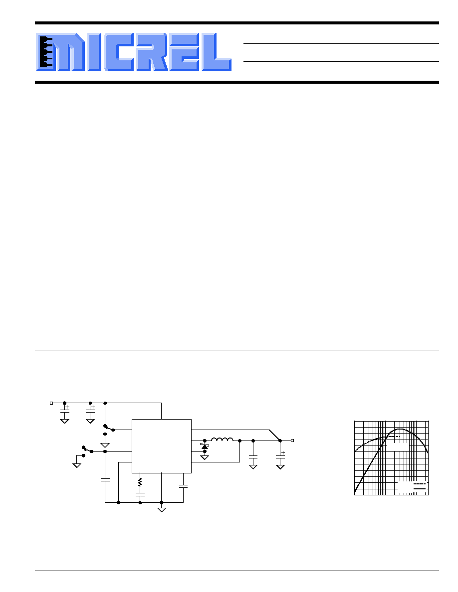
Typical Application
Features
∑ 4.5V to 16.5V input voltage range
∑ Dual-mode operation for high efficiency (up to 96%)
PWM mode for > 200mA load current
Skip mode for < 200mA load current
∑ 100m
internal power MOSFETs at 12V input
∑ 200kHz preset switching frequency
∑ Low quiescent current
1.0mA in PWM mode
500
µ
A in skip mode
< 5
µ
A in shutdown mode
∑ 100% duty cycle for low dropout operation
∑ Current-mode control
Simplified loop compensation
Superior line regulation
∑ Current limit
∑ Thermal shutdown
∑ Undervoltage lockout
Applications
∑ High-efficiency, battery-powered supplies
∑ Buck (step-down) dc-to-dc converters
∑ Cellular telephones
∑ Laptop computers
∑ Hand-held instruments
∑ Battery Charger
BIAS
SGND
EN
COMP
PGND
FB
OUT
VIN
C3
220µF
10V
V
OUT
5V/2.5A
L1, 33µH
C5
10nF
C4
0.01µF
MIC2177-5.0
AUTO
SYNC
R7
15k
V
IN
6V to 16.5V
C1
22µF
35V
U1
20
18
11
13
14≠17
19
12
4≠7
3,8
1,2,9
D1
MBRS140
SW
10
ENABLE
ON
C6
2.2nF
AUTO
MODE
PWM
MODE
Mode
OFF
C2
22µF
35V
C7
220µF
10V
70
75
80
85
90
95
100
10
100
1000 2500
EFFICIENCY (%)
OUTPUT CURRENT (mA)
5V Output
Efficiency
V
IN
= 6V
SKIP
PWM

MIC2177
Micrel
MIC2177
2
April 1999
Ordering Information
Part
Output
Switching
Temperature
Number
Voltage
Frequency
Range
Package
MIC2177-3.3BWM
3.3V
200kHz
≠40
∞
C to +85
∞
C
20-lead wide SOP
MIC2177-5.0BWM
5.0V
200kHz
≠40
∞
C to +85
∞
C
20-lead wide SOP
MIC2177BWM
adj.
200kHz
≠40
∞
C to +85
∞
C
20-lead wide SOP
Pin Description
Pin Number
Pin Name
Pin Function
1, 2, 9
VIN
Supply Input: Controller and switch supply. Unregulated supply input to
internal regulator, output switches, and control circuitry. Requires bypass
capacitor to PGND. All three pins must be connected to V
IN
.
3,8
SW
Switch (Output): Internal power MOSFET switch output. Both pins must be
externally connected together.
4,5,6,7
PGND
Power Ground: Output stage ground connections. Connect all pins to a
common ground plane.
10
OUT
Output Voltage Sense (Input): Senses output voltage to determine minimum
switch current for PWM operation. Connect directly to V
OUT
.
11
AUTO
Automatic Mode: Connect 2.2nF timing capacitor for automatic PWM-/skip-
mode switching. Regulator operates exclusively in PWM mode when pin is
pulled low.
12
FB
Feedback (Input): Error amplifier inverting input. For adjustable output
version, connect FB to external resistive divider to set output voltage. For
3.3V and 5V fixed output versions, connect FB directly to output.
13
COMP
Compensation: Internal error amplifier output. Connect to capacitor or series
RC network to compensate the regulator control loop.
14,15,16,17
SGND
Signal Ground: Ground connection of control section. Connect all pins to
common ground plane.
18
SYNC
Frequency Synchronization (Input): Optional clock input. Connect to
external clock signal to synchronize oscillator. Leading edge of signal above
1.7V terminates switching cycle. Connect to SGND if not used.
19
BIAS
Bias Supply: Internal 3.3V bias supply output. Decouple with 0.01
µ
F
bypass capacitor to SGND. Do not apply any external load.
20
EN
Enable (Input): Logic high enables operation. Logic low shuts down
regulator. Do not allow pin to float.
Pin Configuration
2
VIN
3
SW
4
PGND
5
PGND
6
PGND
7
PGND
1
VIN
8
SW
9
VIN
EN
20
BIAS
19
SYNC
18
SGND
17
SGND
16
SGND
15
10
OUT
14
13
12
11 AUTO
FB
COMP
SGND
20-Lead Wide SOP

April 1999
3
MIC2177
MIC2177
Micrel
Absolute Maximum Ratings
Supply Voltage [100ms transient] (V
IN
) ......................... 18V
Output Switch Voltage (V
SW
) ........................................ 18V
Output Switch Current (I
SW
) ......................................... 6.0A
Enable, Output-Sense Voltage (V
EN
, V
OUT
) ................. 18V
Sync Voltage (V
SYNC
) ..................................................... 6V
Operating Ratings
Supply Voltage (V
IN
) ..................................... 4.5V to 16.5V
Junction Temperature Range (T
J
) ........... ≠40
∞
C to +125
∞
C
Electrical Characteristics
V
IN
= 7.0V; T
A
= 25
∞
C, bold indicates ≠40
∞
C
T
A
85
∞
C; unless noted.
Symbol
Parameter
Condition
Min
Typ
Max
Units
I
SS
Input Supply Current
PWM mode, output not switching,
1.0
1.5
mA
4.5V
V
IN
16.5V
skip mode, output not switching,
500
650
µ
A
4.5V
V
IN
16.5V
V
EN
= 0V, 4.5V
V
IN
16.5V
1
25
µ
A
V
BIAS
Bias Regulator Output Voltage
V
IN
= 16.5V
3.10
3.30
3.4
V
V
FB
Feedback Voltage
MIC2177 [adj.]: V
OUT
= 3.3V, I
LOAD
= 0
1.22
1.245
1.27
V
V
OUT
Output Voltage
MIC2177 [adj.]: V
OUT
= 3.3V,
3.20
3.3
3.40
V
5V
V
IN
16V, 10mA
I
LOAD
2A
3.14
3.46
V
MIC2177-5.0: I
LOAD
= 0
4.85
5.0
5.15
V
MIC2177-5.0:
4.85
5.0
5.15
6V
V
IN
16V, 10mA
I
LOAD
2A
4.75
5.25
V
MIC2177-3.3: I
LOAD
= 0
3.20
3.3
3.40
V
MIC2177-3.3:
3.20
3.3
3.40
V
5V
V
IN
16V, 10mA
I
LOAD
2A
3.14
3.46
V
V
TH
Undervoltage Lockout
upper threshold
4.25
4.35
V
V
TL
lower threshold
3.9
4.15
V
I
FB
Feedback Bias Current
MIC2177 [adj.]
60
150
nA
MIC2177-5.0, MIC2177-3.3
20
40
µ
A
A
VOL
Error Amplifier Gain
0.6V
V
COMP
0.8V
15
18
20
Error Amplifier Output Swing
upper limit
0.9
1.5
V
lower limit
0.05
0.1
V
Error Amplifier Output Current
source and sink
15
25
35
µ
A
f
O
Oscillator Frequency
160
200
240
kHz
D
MAX
Maximum Duty Cycle
V
FB
= 1.0V
100
%
t
ON min
Minimum On-Time
V
FB
= 1.5V
300
400
ns
SYNC Frequency Range
220
300
kHz
SYNC Threshold
0.8
1.6
2.2
V
SYNC Minimum Pulse Width
500
ns
I
SYNC
SYNC Leakage
V
SYNC
= 0V to 5.5V
≠1
0.01
1
µ
A
I
LIM
Current Limit
PWM mode, V
IN
= 12V
3.8
4.7
5.7
A
skip mode
600
mA
R
ON
Switch On-Resistance
high-side switch, V
IN
= 12V
90
250
m
low-side switch, V
IN
= 12V
110
250
m
I
SW
Output Switch Leakage
V
SW
= 16.5V
1
10
µ
A

MIC2177
Micrel
MIC2177
4
April 1999
Symbol
Parameter
Condition
Min
Typ
Max
Units
Enable Threshold
0.8
1.6
2.2
V
I
EN
Enable Leakage
V
EN
= 0V to 5.5V
≠1
0.01
1
µ
A
AUTO Threshold
0.8
1.6
V
AUTO Source Current
V
FB
= 1.5V, V
AUTO
< 0.8V
7
11
15
µ
A
Minimum Switch Current
V
IN
≠ V
OUT
= 0V
220
mA
for PWM Operation
V
IN
≠ V
OUT
= 3V
420
mA
General Note: Devices are ESD sensitive. Handling precautions recommended.

April 1999
5
MIC2177
MIC2177
Micrel
Typical Characteristics
175
180
185
190
195
200
205
-60 -30
0
30
60
90 120 150
FREQUENCY (kHz)
TEMPERATURE (
∞
C)
Oscillator Frequency
vs. Temperature
1.238
1.240
1.242
1.244
1.246
1.248
1.250
1.252
-60 -30
0
30
60
90 120 150
REFERENCE VOLTAGE (V)
TEMPERATURE (
∞
C)
Reference Voltage
vs. Temperature
MIC2177 [adj.]
3.280
3.285
3.290
3.295
3.300
3.305
3.310
3.315
3.320
-60 -30
0
30
60
90 120 150
REFERENCE VOLTAGE (V)
TEMPERATURE (
∞
C)
Reference Voltage
vs. Temperature
MIC2177-3.3
4.970
4.980
4.990
5.000
5.010
5.020
5.030
-60 -30
0
30
60
90 120 150
REFERENCE VOLTAGE (V)
TEMPERATURE (
∞
C)
Reference Voltage
vs. Temperature
MIC2177-5.0
16.0
16.5
17.0
17.5
18.0
18.5
19.0
-60 -30
0
30
60
90 120 150
AMPLIFIER VOLTAGE GAIN
TEMPERATURE (
∞
C)
Error-Amplifier Gain
vs. Temperature
0
20
40
60
80
100
120
-60 -30
0
30
60
90 120 150
BIAS CURRENT (nA)
TEMPERATURE (
∞
C)
Feedback Input Bias Current
vs. Temperature
4.0
4.1
4.2
4.3
4.4
4.5
4.6
4.7
4.8
4.9
5.0
-60 -30
0
30
60
90 120 150
CURRENT LIMIT (A)
TEMPERATURE (
∞
C)
Current Limit
vs. Temperature
0
50
100
150
200
250
2
4
6
8
10 12 14 16 18
ON-RESISTANCE (m
)
INPUT VOLTAGE (V)
High-Side Switch
On-Resistance
125
∞
C
85
∞
C
25
∞
C
0
∞
C
0
50
100
150
200
250
300
350
2
4
6
8
10 12 14 16 18
ON-RESISTANCE (m
)
INPUT VOLTAGE (V)
Low-Side Switch
On-Resistance
125
∞
C
85
∞
C
25
∞
C
0
∞
C
0
2
4
6
8
10
12
2
4
6
8
10 12 14 16 18
SUPPLY CURRENT (mA)
INPUT VOLTAGE (V)
PWM-Mode
Supply Current
OUTPUT
SWITCHING
60
65
70
75
80
85
90
95
100
10
100
1000 2500
EFFICIENCY (%)
OUTPUT CURRENT (mA)
V
IN
= 5V
8V
12V
3.3V Output
Efficiency
SKIP
PWM
70
75
80
85
90
95
100
10
100
1000 2500
EFFICIENCY (%)
OUTPUT CURRENT (mA)
8V
12V
5V Output
Efficiency
V
IN
= 6V
SKIP
PWM
MIC2177
Micrel
MIC2177
6
April 1999
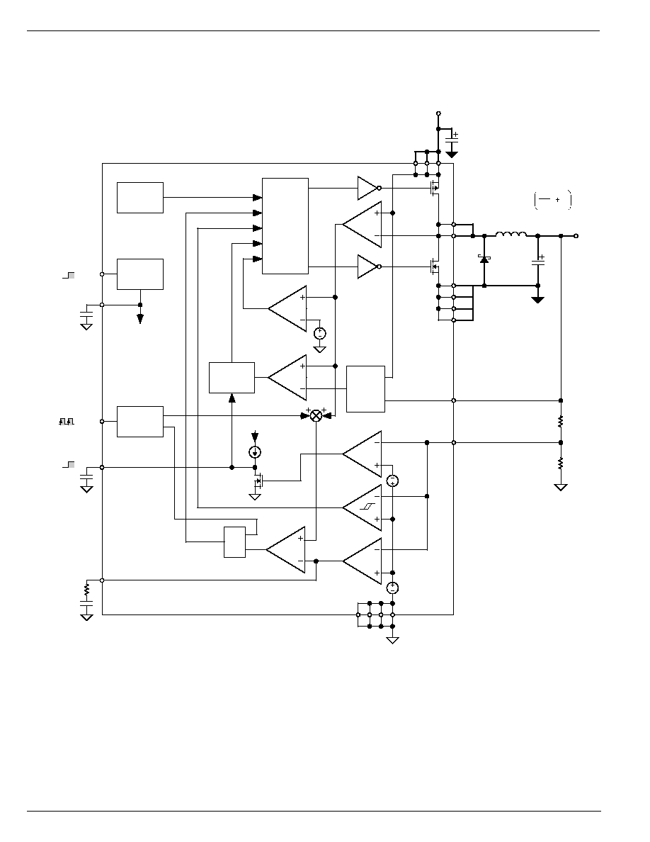
Block Diagram
V
OUT
1.245
R1
R2
1
SW
PGND
I
SENSE
Amp.
PWM/
Skip-Mode
Select Logic
V
REF
1.245V
FB
100m
N-channel
100m
P-channel
COMP
VIN
Error
Amp.
Skip-Mode
Comp.
I
MIN
Comp.
I
LIMIT
Comp.
Output
Control
Logic
I
MIN
Thrshld.
Low Output
Comp.
40mV
R
S
Q
200kHz
Oscillator
PWM
Comp.
3.3V
Regulator
UVLO,
Thermal
Shutdown
V
OUT
L1
OUT
SGND
2.2nF
C
C
AUTO
0.01µF
EN
BIAS
V
IN
4.5V to 16.5V
C
IN
SYNC
C
OUT
MIC2177 [Adjustable]
internal
supply
voltage
Enable
Shutdown
Auto-Mode
PWM
20
19
18
11
13
2
1
3
8
D
4
5
6
7
R1
R2
12
10
14
15
16
17
Bold lines indicate
high current traces
R
C
CORRECTIVE RAMP
RESET PULSE
10µA
3.3V
9

April 1999
7
MIC2177
MIC2177
Micrel
Functional Description
Micrel's MIC2177 is a synchronous buck regulator that oper-
ates from an input voltage of 4.5V to 16.5V and provides a
regulated output voltage of 1.25V to 16.5V. It has internal
power MOSFETs that supply up to 2.5A of load current and
operates with up to 100% duty cycle to allow low-dropout
operation. To optimize efficiency, the MIC2177 operates in
PWM and skip mode. Skip mode provides the best efficiency
when load current is less than 200mA, while PWM mode is
more efficient at higher current. A patented technique allows
the MIC2177 to automatically select the correct operating
mode as the load current changes.
During PWM operation, the MIC2177 uses current-mode
control which provides superior line regulation and makes the
control loop easier to compensate. The PWM switching
frequency is set internally to 200kHz and can be synchro-
nized to an external clock frequency up to 300kHz. Other
features include a low-current shutdown mode, current limit,
undervoltage lockout, and thermal shutdown. See the follow-
ing sections for details.
Switch Output
The switch output (SW) is a half H-bridge consisting of a high-
side P-channel and low-side N-channel power MOSFET.
These MOSFETs have a typical on-resistance of 100m
when the MIC2177 operates from a 12V supply. Antishoot-
through circuitry prevents the P-channel and N-channel from
turning on at the same time.
Current Limit
The MIC2177 uses pulse-by-pulse current limiting to protect
the output. During each switching period, a current limit
comparator detects if the P-channel current exceeds 4.7A.
When it does, the P-channel is turned off until the next
switching period begins.
Undervoltage Lockout
Undervoltage lockout (UVLO) turns off the output when the
input voltage (V
IN
) is too low to provide sufficient gate drive for
the output MOSFETs. It prevents the output from turning on
until V
IN
exceeds 4.3V. Once operating, the output will not
shut off until V
IN
drops below 4.2V.
Thermal Shutdown
Thermal shutdown turns off the output when the MIC2177
junction temperature exceeds the maximum value for safe
operation. After thermal shutdown occurs, the output will not
turn on until the junction temperature drops approximately
10
∞
C.
Shutdown Mode
The MIC2177 has a low-current shutdown mode that is
controlled by the enable input (EN). When a logic 0 is applied
to EN, the MIC2177 is in shutdown mode and its quiescent
current drops to less than 5
µ
A.
Internal Bias Regulator
An internal 3.3V regulator provides power to the MIC2177
control circuits. This internal supply is brought out to the BIAS
pin for bypassing by an external 0.01
µ
F capacitor. Do not
connect any external load to the BIAS pin. It is not designed
to provide an external supply voltage.
Frequency Synchronization
The MIC2177 operates at a preset switching frequency of
200kHz. It can be synchronized to a higher frequency by
connecting an external clock to the SYNC pin. The SYNC pin
is a logic level input that synchronizes the oscillator to the
rising edge of an external clock signal. It has a frequency
range of 220kHz≠300kHz, and can operate with a minimum
pulse-width of 500ns. If synchronization is not required,
connect SYNC to ground.
Low-Dropout Operation
Output regulation is maintained in PWM or skip mode even
when the difference between V
IN
and V
OUT
decreases below
1V. As V
IN
≠ V
OUT
decreases, the duty cycle increases until
it reaches 100%. At this point, the P-channel is kept on for
several cycles at a time, and the output stays in regulation
until V
IN
≠ V
OUT
falls below the dropout voltage (dropout
voltage = P-channel on resistance
◊
load current).
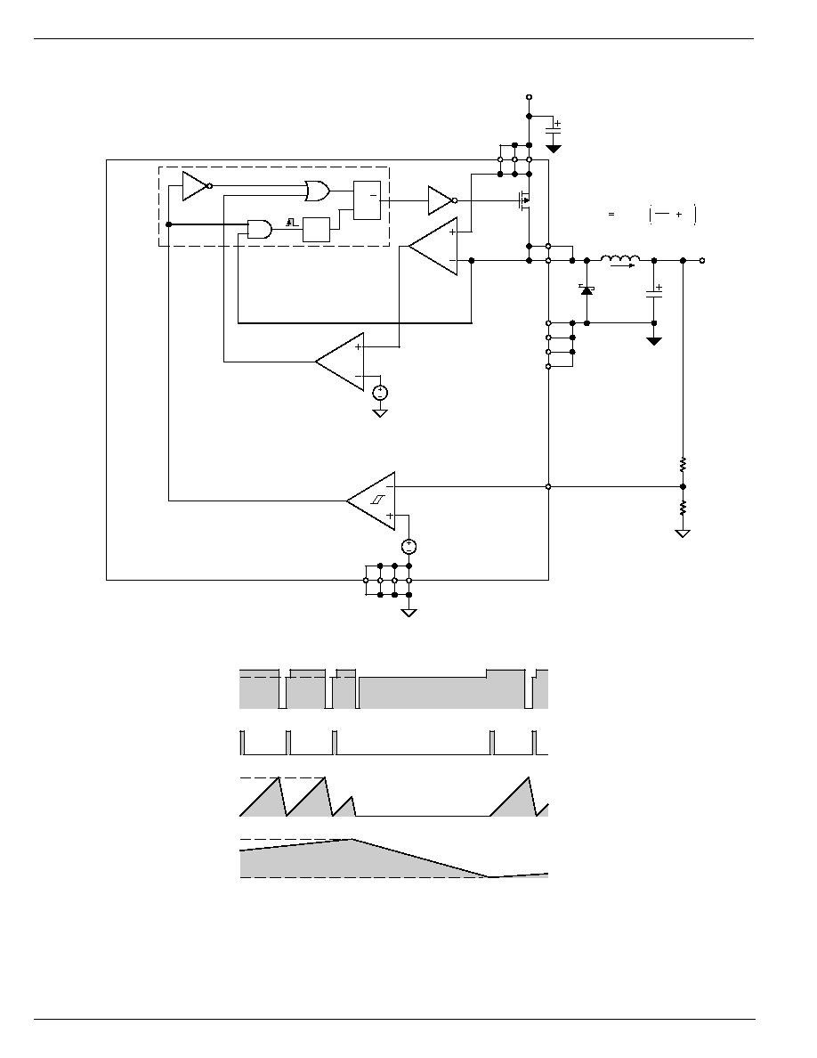
PWM-Mode Operation
Refer to "PWM-Mode Functional Diagram" which is a simpli-
fied block diagram of the MIC2177 operating in PWM mode
with its associated waveforms.
When operating in PWM mode, the output P-channel and N-
channel MOSFETs are alternately switched on at a constant
frequency and variable duty cycle. A switching period begins
when the oscillator generates a reset pulse. This pulse resets
the RS latch which turns on the P-channel and turns off the
N-channel. During this time, inductor current (I
L1
) increases
and energy is stored in the inductor. The current sense
amplifier (I
SENSE
Amp) measures the P-channel drain-to-
source voltage and outputs a voltage proportional to I
L1
. The
output of I
SENSE
Amp is added to a sawtooth waveform
(corrective ramp) generated by the oscillator, creating a
composite waveform labeled I
SENSE
on the timing diagram.
When I
SENSE
is greater than the error amplifier output, the
PWM comparator will set the RS latch which turns off the P-
channel and turns on the N-channel. Energy is then dis-
charged from the inductor and I
L1
decreases until the next
switching cycle begins. By varying the P-channel on-time
(duty cycle), the average inductor current is adjusted to
whatever value is required to regulate the output voltage.
The MIC2177 uses current-mode control to adjust the duty
cycle and regulate the output voltage. Current-mode control
has two signal loops that determine the duty cycle. One is an
outer loop that senses the output voltage, and the other is a
faster inner loop that senses the inductor current. Signals
from these two loops control the duty cycle in the following
way: V
OUT
is fed back to the error amplifier which compares
the feedback voltage (V
FB
) to an internal reference voltage
(V
REF
). When V
OUT
is lower than its nominal value, the error
amplifier output voltage increases. This voltage then inter-
sects the current-sense waveform later in switching period
which increases the duty cycle and average inductor current.
If V
OUT
is higher than nominal, the error amplifier output
voltage decreases, reducing the duty cycle.
The PWM control loop is stabilized in two ways. First, the
inner signal loop is compensated by adding a corrective ramp
to the output of the current sense amplifier. This allows the
regulator to remain stable when operating at greater than

MIC2177
Micrel
MIC2177
8
April 1999
50% duty cycle. Second, a series resistor-capacitor load is
connected to the error amplifier output (COMP pin). This
places a pole-zero pair in the regulator control loop.
One more important item is synchronous rectification. As
mentioned earlier, the N-channel output MOSFET is turned
on after the P-channel turns off. When the N-channel turns
on, its on-resistance is low enough to create a short across
the output diode. As a result, inductor current flows through
the N-channel and the voltage drop across it is significantly
lower than a diode forward voltage. This reduces power
dissipation and improves efficiency to greater than 95%
under certain operating conditions.
To prevent shoot through current, the output stage employs
break-before-make circuitry that provides approximately 50ns
of delay from the time one MOSFET turns off and the other
turns on. As a result, inductor current briefly flows through the
output diode during this transition.
Skip-Mode Operation
Refer to "Skip-Mode Functional Diagram" which is a simpli-
fied block diagram of the MIC2177 operating in skip mode
and its associated waveforms.
Skip-mode operation turns on the output P-channel at a
frequency and duty cycle that is a function of V
IN
, V
OUT
, and
the output inductor value. While in skip mode, the N-channel
is kept off to optimize efficiency by reducing gate charge
dissipation. V
OUT
is regulated by skipping switching cycles
that turn on the P-channel.
To begin analyzing MIC2177 skip-mode operation, assume
the skip-mode comparator output is high and the latch output
has been reset to a logic 1. This turns on the P-channel and
causes I
L1
to increase linearly until it reaches a current limit
of 600mA. When I
L1
reaches this value, the current limit
comparator sets the RS latch output to logic 0, turning off the
P-channel. The output switch voltage (V
SW
) then swings from
V
IN
to 0.4V below ground, and I
L1
flows through the Schottky
diode. L1 discharges its energy to the output and I
L1
de-
creases to zero. When I
L1
= 0, V
SW
swings from ≠0.4V to
V
OUT
, and this triggers a one-shot that resets the RS latch.
Resetting the RS latch turns on the P-channel, which begins
another switching cycle.
The skip-mode comparator regulates V
OUT
by controlling
when the MIC2177 skips cycles. It compares V
FB
to V
REF
and
has 10mV of hysteresis to prevent oscillations in the control
loop. When V
FB
is less than V
REF
≠ 5mV, the comparator
output is logic 1, allowing the P-channel to turn on. Con-
versely, when V
FB
is greater than V
REF
+ 5mV, the P-channel
is turned off.
Note that this is a self-oscillating topology which explains
why the switching frequency and duty cycle are a function of
V
IN
, V
OUT
, and the value of L1. It has the unique feature (for
a pulse-skipping regulator) of supplying the same value of
maximum load current for any value of V
IN
, V
OUT
, or L1. This
allows the MIC2177 to always supply up to 300mA of load
current (I
LOAD
) when operating in skip mode.
Changing from PWM to Skip Mode
Refer to "Block Diagram" for circuits described in the following
sections.
The MIC2177 automatically changes from PWM to skip mode
operation when I
LOAD
drops below a minimum value. I
MIN
is
determined indirectly by detecting when the peak inductor
current (I
L(peak)
) is less than 420mA. This is done by the
minimum current comparator which detects if the output P-
Channel current equals 420mA during each switching cycle.
If it does not, the PWM/skip-mode select logic places the
MIC2177 into skip-mode operation.
The value of I
MIN
that corresponds to I
L1(peak)
= 420mA is
given by the following equation:
I
420mA I
MIN
L1
=
-
2
Where:
I
L1
= inductor ripple current
This equation shows I
MIN
varies as a function of
I
L
. There-
fore, the user must select an inductor value that results in
I
MIN
= 200mA when I
L(peak)
= 420mA. The formulas for cal-
culating the correct inductor value are given in the "Applica-
tions Information" section. Note that
I
L
varies as a function
of input voltage, and this also causes I
MIN
to vary. In applica-
tions where the input voltage changes by a factor of two, I
MIN
will typically vary from 130mA to 250mA.
During low-dropout operation, the minimum current thresh-
old circuit reduces the minimum value of I
L1(peak)
for PWM
operation. This compensates for
I
L1
decreasing to almost
zero when the difference between V
IN
and V
OUT
is very low.
Changing from Skip to PWM Mode
The MIC2177 will automatically change from skip to PWM
mode when I
LOAD
exceeds 300mA. During skip-mode opera-
tion, it can supply up to 300mA, and when I
LOAD
exceeds this
limit, V
OUT
will fall below its nominal value. At this point, the
MIC2177 begins operating in PWM mode. Note that the
maximum value of I
LOAD
for skip mode is greater than the
minimum value required for PWM mode. This current hyster-
esis prevents the MIC2177 from toggling between modes
when I
LOAD
is in the range of 100mA to 300mA.
The low output comparator determines when V
OUT
is low
enough for the regulator to change operating modes. It
detects when the feedback voltage is 3% below nominal, and
pulls the AUTO pin to ground. When AUTO is less than 1.6V,
the PWM/skip-mode select logic places the MIC2177 into
PWM operation. The external 2.2nF capacitor connected to
AUTO is charged by a 10
µ
A current source after the regulator
begins operating in PWM mode. As a result, AUTO stays
below 1.6V for several switching cycles after PWM operation
begins, forcing the MIC2177 to remain in PWM mode during
this transition.
External PWM-Mode Selection
The MIC2177 can be forced to operate in only PWM mode by
connecting AUTO to ground. This prevents skip-mode opera-
tion in applications that are sensitive to switching noise.

April 1999
9
MIC2177
MIC2177
Micrel
PWM-Mode Functional Diagram
SW
PGND
I
SENSE
Amp.
V
REF
1.245V
100m
N-channel
100m
P-channel
COMP
VIN
Error
Amp.
R
S
Q
200kHz
Oscillator
PWM
Comp.
V
OUT
L1
FB
SGND
C
C
V
IN
4.5V to 16.5V
C
IN
SYNC
C
OUT
MIC2177 [Adjustable] PWM-Mode Signal Path
Stop
18
13
2
1
3
8
D
4
5
6
7
R1
R2
12
14
15
16
17
R
C
Corrective
Ramp
Reset
Pulse
I
L1
V
OUT
1.245
R1
R2
1
9
V
SW
I
L1
Reset
Pulse
I
SENSE
I
LOAD
I
L1
Error Amp.
Output
MIC2177
Micrel
MIC2177
10
April 1999
Skip-Mode Functional Diagram
S
R
Q
One
Shot
SW
PGND
I
SENSE
Amp.
V
REF
1.245V
100m
P-channel
VIN
Skip-Mode
Comp.
I
LIMIT
Comp.
V
OUT
L1
FB
SGND
V
IN
4.5V to 16.5V
C
IN
C
OUT
MIC2177 [Adjustable] Skip-Mode Signal Path
2
1
3
8
D
4
5
6
7
R1
R2
12
14
15
16
17
I
LIMIT
Thresh.
Voltage
Output Control Logic
I
L1
V
OUT
1.245
R1
R2
1
9
V
SW
I
L1
One-Shot
Pulse
V
FB
V
REF
+ 5mV
V
REF
≠ 5mV
0
I
LIM
0
V
OUT
V
IN

April 1999
11
MIC2177
MIC2177
Micrel
Application Information
Feedback Resistor Selection (Adjustable Version)
The output voltage is configured by connecting an external
resistive divider to the FB pin as shown in "MIC2177 Block
Diagram." The ratio of R1 to R2 determines the output
voltage. To optimize efficiency during low output current
operation, R2 should not be less than 20k
. However, to
prevent feedback error due to input bias current at the FB pin,
R2 should not be greater than 100k
. After selecting R2,
calculate R1 using the following formula:
R1 = R2
V
1.245V
1
OUT
-
Input Capacitor Selection
The input capacitor is selected for its RMS current and
voltage rating and should be a low ESR (equivalent series
resistance) electrolytic or tantalum capacitor. As a rule-of-
thumb, the voltage rating for a tantalum capacitor should be
twice the value of V
IN
, and the voltage rating for an electrolytic
should be 40% higher than V
IN.
The RMS current rating must
be equal or greater than the maximum RMS input ripple
current. A simple, worst-case formula for calculating this
RMS current is:
I
=
I
RMS(max)
LOAD(max)
2
Tantalum capacitors are a better choice for applications that
require the most compact layout or operation below 0
∞
C. The
input capacitor must be located very close to the VIN pin
(within 0.2 inches, 5mm). Also place a 0.1
µ
F ceramic bypass
capacitor as close as possible to VIN.
Inductor Selection
The inductor must be at least a minimum value in order for the
MIC2177 to change from PWM to skip mode at the correct
value of output current. This minimum value ensures the
inductor ripple current never exceeds 600mA, and is calcu-
lated using the following formula:
L
= V
1 ≠
V
V
8.3 H/V
MIN
OUT
OUT
IN(max)
◊
µ
Where:
V
IN(max)
= maximum input voltage
In general, a value at least 20% greater than L
MIN
should be
selected because inductor values have a tolerance of
±
20%.
Two other parameters to consider in selecting an inductor are
winding resistance and peak current rating. The inductor
must have a peak current rating equal or greater than the
peak inductor current. Otherwise, the inductor may saturate,
causing excessive current in the output switch. Also, the
inductor's core loss may increase significantly. Both of these
effects will degrade efficiency. The formula for peak inductor
current is:
I
I
300mA
L(peak)
LOAD(max)
=
+
To maximize efficiency, the inductor's resistance must be
less than the output switch on-resistance (preferably 50m
or less).
Output Capacitor Selection
Select an output capacitor that has a low value of ESR. This
parameter determines a regulator's output ripple voltage
(V
RIPPLE
) which is generated by
I
L
◊
ESR. As mentioned in
"Inductor Selection," the maximum value for
I
L
is 600mA.
Therefore, the maximum value of ESR is:
ESR
=
600mA
V
MAX
RIPPLE
Where:
V
RIPPLE
< 1% of V
OUT
Typically, capacitors in the range of 100
µ
F to 220
µ
F have
ESR less than this maximum value. The output capacitor can
be either a low ESR electrolytic or tantalum capacitor, but
tantalum is a better choice for compact layout and operation
at temperatures below 0
∞
C. The voltage rating of a tantalum
capacitor must be 2
◊
V
OUT
, and the voltage rating of an
electrolytic must be 1.4
◊
V
OUT
.
Output Diode Selection
In PWM operation, inductor current flows through the output
diode approximately 50ns during the dead time when one
output MOSFET turns off and the other turns on. In skip
mode, the inductor current flows through the diode during the
entire P-channel off time. The correct diode for both of these
conditions is a 1A diode with a reverse voltage rating greater
than V
IN
. It must be a Schottky or ultrafast-recovery diode
(t
R
< 100ns) to minimize power dissipation from the diode's
reverse-recovery charge.
Compensation
Compensation is provided by connecting a series RC load to
the COMP pin. This creates a pole-zero pair in the regulator
control loop, allowing the regulator to remain stable with
enough low frequency loop-gain for good load and line
regulation. At higher frequencies, pole-zero reduces loop-
gain to a level referred to as the mid-band gain. The mid-band
gain is low enough so that the loop gain crosses 0dB with
sufficient phase margin. Typical values for the RC load are
4.7nF ≠ 10nF for the capacitor and 5k
≠ 20k
for the
resistor.
Printed Circuit Board Layout
A well designed PC board will prevent switching noise and
ground bounce from interfering with the operation of the
MIC2177. A good design takes into consideration component
placement and routing of power traces.
The first thing to consider is the locations of the input
capacitor, inductor, output diode, and output capacitor. The
input capacitor must be placed very close to the VIN pin, the
inductor and output diode very close to the SW pin, and the
output capacitor near the inductor. These components pass
large high-frequency current pulses, so they must use short,
wide power traces. In addition, their ground pins and PGND
are connected to a ground plane that is nearest the power
supply ground bus.

MIC2177
Micrel
MIC2177
12
April 1999
The feedback resistors, RC compensation network, and
BIAS pin bypass capacitor should be located near their
respective pins. To prevent ground bounce, their ground
traces and SGND should not be in the path of switching
currents returning to the power supply ground bus. SGND
and PGND should be tied together by a ground plane that
extends under the MIC2177.
BIAS
SGND
AUTO
COMP
PGND
FB
SW
VIN
C2
100µF
10V
V
OUT
3.3V/1A
L1, 50µH
C4
6.8nF
C3
0.01µF
MIC2177
SYNC
EN
R4
10k
V
IN
4.5V to 16.5V
C1
22µF
35V
U1
20
18
10
11
13
14≠17
19
12
4≠7
3,8
1,2,9
D1
MBRS130L
U1 Micrel
MIC2177-3.3BWM
C1 AVX
TPSE226M035R0300, ESR = 0.3
C2 AVX
TPSD107M010R0100, ESR = 0.1
C3 Z5UorX7R Ceramic Dielectric Material
C4 X7RorNP0 Ceramic Dielectric Material
D1 Motorola
MBRS130LT3
L1
Coiltronics CTX50-4P, DCR = 0.097
L1
Coilcraft
DO3316P-473, DCR = 0.12
L1
Bi
HM77-11003, DCR = 0.073
C5
0.01
µF
OUT
Figure 1. MIC2177 4.5V≠16.5V to 3.3/1A Regulator
Suggested Manufacturers List
Inductors
Capacitors
Diodes
Transistors
Coilcraft
AVX Corp.
General Instruments (GI)
Siliconix
1102 Silver Lake Rd.
801 17th Ave. South
10 Melville Park Rd.
2201 Laurelwood Rd.
Cary, IL 60013
Myrtle Beach, SC 29577
Melville, NY 11747
Santa Clara, CA 96056
tel: (708) 639-2361
tel: (803) 448-9411
tel: (516) 847-3222
tel: (800) 554-5565
fax: (708) 639-1469
fax: (803) 448-1943
fax: (516) 847-3150
Coiltronics
Sanyo Video Components Corp.
International Rectifier Corp.
6000 Park of Commerce Blvd.
2001 Sanyo Ave.
233 Kansas St.
Boca Raton, FL 33487
San Diego, CA 92173
El Segundo, CA 90245
tel: (407) 241-7876
tel: (619) 661-6835
tel: (310) 322-3331
fax: (407) 241-9339
fax: (619) 661-1055
fax: (310) 322-3332
Bi Technologies
Sprague Electric
Motorola Inc.
4200 Bonita Place
Lower Main St.
MS 56-126
Fullerton, CA
60005 Sanford, ME 04073
3102 North 56th St.
tel: (714) 447-2345
tel: (207) 324-4140
Phoenix, AZ 85018
fax: (714) 447-2500
tel: (602) 244-3576
fax: (602) 244-4015

April 1999
13
MIC2177
MIC2177
Micrel
Package Information
0.022 (0.559)
0.018 (0.457)
5
∞
TYP
0.408 (10.363)
0.404 (10.262)
0.509 (12.929)
0.505 (12.827)
0.103 (2.616)
0.099 (2.515)
SEATING
PLANE
0.027 (0.686)
0.031 (0.787)
0.016 (0.046)
TYP
0.301 (7.645)
0.297 (7.544)
0.094 (2.388)
0.090 (2.286)
0.297 (7.544)
0.293 (7.442)
10
∞
TYP
0.032 (0.813) TYP
0.330 (8.382)
0.326 (8.280)
7
∞
TYP
0.050 (1.270)
TYP
0.015
(0.381)
R
0.015
(0.381)
MIN
PIN 1
DIMENSIONS:
INCHES (MM)
20-Lead Wide SOP (WM)

MIC2177
Micrel
MIC2177
14
April 1999

April 1999
15
MIC2177
MIC2177
Micrel

MIC2177
Micrel
MIC2177
16
April 1999
MICREL INC.
1849 FORTUNE DRIVE
SAN JOSE, CA 95131
USA
TEL
+ 1 (408) 944-0800
FAX
+ 1 (408) 944-0970
WEB
http://www.micrel.com
This information is believed to be accurate and reliable, however no responsibility is assumed by Micrel for its use nor for any infringement of patents or
other rights of third parties resulting from its use. No license is granted by implication or otherwise under any patent or patent right of Micrel Inc.
© 1999 Micrel Incorporated