June 2000
1
MIC2182
MIC2182
Micrel
MIC2182
High-Efficiency Synchronous Buck Controller
Final Information
General Description
Micrel's MIC2182 is a synchronous buck (step-down) switch-
ing regulator controller. An all N-channel synchronous archi-
tecture and powerful output drivers allow up to a 20A output
current capabilty. The PWM and skip-mode control scheme
allows efficiency to exceed 95% over a wide range of load
current, making it ideal for battery powered applications, as
well as high current distributed power supplies.
The MIC2182 operates from a 4.5V to 32V input and can
operate with a maximum duty cycle of 86% for use in low-
dropout conditions. It also features a shutdown mode that
reduces quiescent current to 0.1
µ
A.
The MIC2182 achieves high efficiency over a wide output
current range by automatically switching between PWM and
skip mode. Skip-mode operation enables the converter to
maintain high efficiency at light loads by turning off circuitry
pertaining to PWM operation, reducing the no-load supply
current from 1.6mA to 600
µ
A. The operating mode is inter-
nally selected according to the output load conditions. Skip
mode can be defeated by pulling the PWM pin low which
reduces noise and RF interference.
The MIC2182 is available in a 16-pin SOP (small-outline
package) and SSOP (shrink small-outline package) with an
operating range from ≠40
∞
C to +85
∞
C.
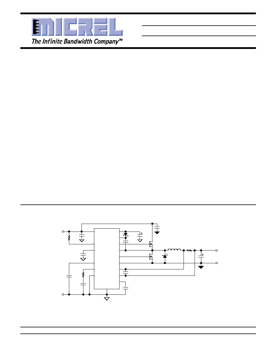
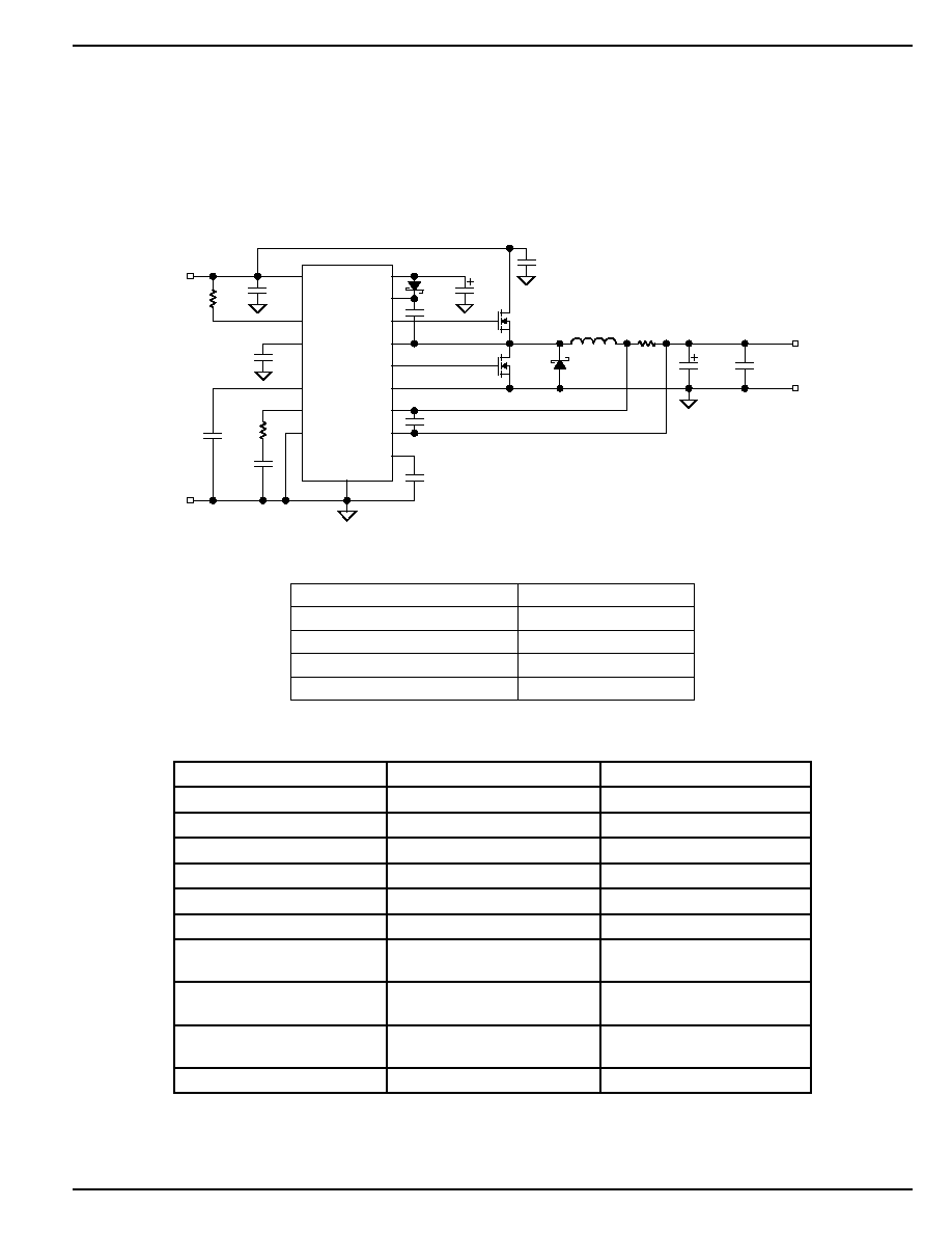
Typical Application
VDD
BST
C6
0.1
µ
F
R1
2k
R7
100k
V
IN
4.5V to 30V*
V
OUT
3.3V/4A
GND
C2
2.2nF
C4
1nF
C3
0.1
µ
F
C5
0.1
µ
F
C1
0.1
µ
F
C9
4.7
µ
F
16V
C11
22uf
35V
x2
D2
SD103BWS
Q2*
Si4884
D1
B140
C7
220uf
10V
◊
2
L1
10
µ
H
R2
0.02
Q1*
Si4884
HSD
VSW
LSD
PGND
CSH
VOUT
VREF
SGND
GND
MIC2182-3.3BSM
VIN
EN/UVLO
SS
PWM
COMP
SYNC
C13, 1nF
10
6
2
1
3
5
4
7
9
8
12
13
15
16
14
11
* 30V maximum input voltage limit is due
to standard 30V MOSFET selection.
See "Application Information" section for
5V to 3.3V/10A and other circuits.
4.5V≠30V* to 3.3V/4A Converter
Micrel, Inc. ∑ 1849 Fortune Drive ∑ San Jose, CA 95131 ∑ USA ∑ tel + 1 (408) 944-0800 ∑ fax + 1 (408) 944-0970 ∑ http://www.micrel.com
Features
∑ 4.5V to 32V Input voltage range
∑ 1.25V to 6V Output voltage range
∑ 95% efficiency
∑ 300kHz oscillator frequency
∑ Current sense blanking
∑ 5
impedance MOSFET Drivers
∑ Drives N-channel MOSFETs
∑ 600
µ
A typical quiescent current (skip-mode)
∑ Logic controlled micropower shutdown (I
Q
< 0.1
µ
A)
∑ Current-mode control
∑ Cycle-by-cycle current limiting
∑ Built-in undervoltage protection
∑ Adjustable undervoltage lockout
∑ Easily synchronizable
∑ Precision 1.245V reference output
∑ 0.6% total regulation
∑ 16-pin SOP and SSOP packages
∑ Frequency foldback overcurrent protection
∑ Sustained short-circuit protection at any input voltage
∑ 20A output current capability
Applications
∑ DC power distribution systems
∑ Notebook and subnotebook computers
∑ PDAs and mobile communicators
∑ Wireless modems
∑ Battery-operated equipment

MIC2182
Micrel
MIC2182
2
June 2000
Ordering Information
Part Number
Voltage
Temperature Range
Package
MIC2182BM
Adjustable
≠40
∞
C to +85
∞
C
16-pin narrow SOP
MIC2182-3.3BM
3.3V
≠40
∞
C to +85
∞
C
16-pin narrow SOP
MIC2182-5.0BM
5.0V
≠40
∞
C to +85
∞
C
16-pin narrow SOP
MIC2182BSM
Adjustable
≠40
∞
C to +85
∞
C
16-pin narrow SSOP
MIC2182-3.3BSM
3.3V
≠40
∞
C to +85
∞
C
16-pin narrow SSOP
MIC2182-5.0BSM
5.0V
≠40
∞
C to +85
∞
C
16-pin narrow SSOP
Pin Configuration
1
2
3
4
16
15
14
13
HSD
VSW
BST
LSD
SS
PWM
COMP
SGND
MIC2182
5
6
7
8
12
11
10
9
PGND
VDD
VIN
VOUT
SYNC
EN/UVLO
FB
CSH
Adjustable
16-pin SOP (M)
16-Pin SSOP (SM)
1
2
3
4
16
15
14
13
HSD
VSW
BST
LSD
SS
PWM
COMP
SGND
MIC2182-x.x
5
6
7
8
12
11
10
9
PGND
VDD
VIN
VOUT
SYNC
EN/UVLO
VREF
CSH
Fixed
16-pin SOP (M)
16-Pin SSOP (SM)

June 2000
3
MIC2182
MIC2182
Micrel
Pin Description
Pin Number
Pin Name
Pin Function
1
SS
Soft-Start (External Component): Connect external capacitor to ground to
reduce inrush current by delaying and slowing the output voltage rise time.
Rise time is controlled by an internal 5
µ
A current source that charges an
external capacitor to V
DD
.
2
PWM
PWM/Skip-Mode Select (Input): Low sets PWM-mode operation. 1nF
capacitor to ground sets automatic PWM/skip-mode selection.
3
COMP
Compensation (Output): Internal error amplifier output. Connect to capacitor
or series RC network to compensate the regulator control loop.
4
SGND
Small Signal Ground (Return): Route separately from other ground traces to
the (≠) terminal of C
OUT
.
5
SYNC
Frequency Synchronization (Input): Optional. Connect to external clock
signal to synchronize the oscillator. Leading edge of signal above the
threshold terminates the switching cycle. Connect to SGND if unused.
6
EN/UVLO
Enable/Undervoltage Lockout (Input): Low-level signal powers down the
controller. Input below the 2.5V threshold disables switching and functions
as an accurate undervoltage lockout (UVLO). Input below the threshold
forces complete micropower (< 0.1
µ
A) shutdown.
7 (fixed)
VREF
Reference Voltage (Output): 1.245V output. Requires 0.1
µ
f capacitor to
ground.
7 (adj)
FB
Feedback (Input): Regulates FB pin to 1.245V. See "Application Information"
for resistor divider calculations.
8
CSH
Current-Sense High (Input): Current-limit comparator noninverting input. A
built-in offset of 100mV between CSH and V
OUT
pins in conjunction with the
current-sense resistor set the current-limit threshold level. This is also the
positive input to the current sense amplifier.
9
VOUT
Current-Sense Low (Input): Output voltage feedback input and inverting
input for the current limit comparator and the current sense amplifier.
10
VIN
[Battery] Unregulated Input (Input): +4.5V to +32V supply input.
11
VDD
5V Internal Linear-Regulator (Output): V
DD
is the external MOSFET gate
drive supply voltage and an internal supply bus for the IC. Bypass to SGND
with 4.7
µ
F. V
DD
can supply up to 5mA for external loads.
12
PGND
MOSFET Driver Power Ground (Return): Connects to source of synchro-
nous MOSFET and the (≠) terminal of C
IN
13
LSD
Low-Side Drive (Output): High-current driver output for external synchronous
MOSFET. Voltage swing is between ground and V
DD
.
14
BST
Boost (Input): Provides drive voltage for the high-side MOSFET driver. The
drive voltage is higher than the input voltage by V
DD
minus a diode drop.
15
VSW
Switch (Return): High side MOSFET driver return.
16
HSD
High-Side Drive (Output): High-current driver output for high-side MOSFET.
This node voltage swing is between ground and V
IN
+ 5V ≠ V
diode drop
.
MIC2182
Micrel
MIC2182
4
June 2000
Electrical Characteristics
V
IN
= 15V; SS = open; V
PWM
= 0V; V
SHDN
= 5V; I
LOAD
= 0.1A; T
A
= 25
∞
C, bold values indicate ≠40
∞
C
T
A
+85
∞
C; Note 4; unless
noted
Parameter
Condition
Min
Typ
Max
Units
MIC2182 [Adjustable], (Note 5)
Feedback Voltage Reference
1.233
1.245
1.257
V
Feedback Voltage Reference
1.220
1.245
1.270
V
Feedback Voltage Reference
4.5V < V
IN
< 32V, 0 < V
CSH
≠ V
OUT
< 75mV
1.208
1.245
1.282
V
Feedback Bias Current
10
nA
Output Voltage Range
1.25
6
V
Output Voltage Line Regulation
V
IN
= 4.5V to 32V, V
CSH
≠ V
OUT
= 50mV
0.03
%/V
Output Voltage Load Regulation
25mV < (V
CSH
≠ V
OUT
) < 75mV (PWM mode only)
0.5
%
Output Voltage Total Regulation
0mV < (V
CSH
≠ V
OUT
) < 75mV (full load range) 4.5V < V
IN
< 32V
0.6
%
MIC2182-3.3
Output Voltage
3.267
3.3
3.333
V
Output Voltage
3.234
3.3
3.366
V
Output Voltage
4.5V < V
IN
< 32V, 0 < V
CSH
≠ V
OUT
< 75mV
3.201
3.3
3.399
V
Output Voltage Line Regulation
V
IN
= 4.5V to 32V, V
CSH
≠ V
OUT
= 50mV
0.03
%/V
Output Voltage Load Regulation
25mV < (V
CSH
≠ V
OUT
) < 75mV (PWM mode only)
0.5
%
Output Voltage Total Regulation
0mV < (V
CSH
≠ V
OUT
) < 75mV (full load range) 4.5V < V
IN
< 32V
0.8
%
MIC2182-5.0
Output Voltage
4.95
5.0
5.05
V
Output Voltage
4.90
5.0
5.10
V
Output Voltage
6.5V < V
IN
< 32V, 0 < V
CSH
≠ V
OUT
< 75mV
4.85
5.0
5.150
V
Output Voltage Line Regulation
V
IN
= 6.5V to 32V, V
CSH
≠ V
OUT
= 50mV
0.03
%/V
Output Voltage Load Regulation
25mV < (V
CSH
≠ V
OUT
) < 75mV (PWM mode only)
0.5
%
Output Voltage Total Regulation
0mV < (V
CSH
≠ V
OUT
) < 75mV (full load range) 6.5V < V
IN
< 32V
0.8
%
Input and VDD Supply
PWM Mode
V
PWM
= 0V, excluding external MOSFET gate drive current
1.6
2.5
mA
Skip Mode
I
L
= 0mA, V
PWM
floating (1nF capacitor to ground)
600
1500
µ
A
Shutdown Quiescent Current
V
EN/UVLO
= 0V
0.1
5
µ
A
Digital Supply Voltage (V
DD
)
I
L
= 0mA to 5mA
4.7
5.3
V
Undervoltage Lockout
V
DD
upper threshold (turn on threshold)
4.2
V
V
DD
lower threshold (turn off threshold)
4.1
V
Absolute Maximum Ratings
(Note 1)
Analog Supply Voltage (V
IN
) ....................................... +34V
Digital Supply Voltage (V
DD
) ......................................... +7V
Driver Supply Voltage (B
ST
) .................................... V
IN
+7V
Sense Voltage (V
OUT
, C
SH
) ............................. 7V to ≠0.3V
Sync Pin Voltage (V
SYNC
) ................................ 7V to ≠0.3V
Enable Pin Voltage (V
EN/UVLO
) ...................................... V
IN
Power Dissipation (P
D
)
SOP ................................................ 400mW @ T
A
= 85
∞
C
SSOP ............................................. 270mW @ T
A
= 85
∞
C
Ambient Storage Temperature (T
S
) ......... ≠65
∞
C to +150
∞
C
ESD, Note 3
Operating Ratings
(Note 2)
Analog Supply Voltage (V
IN
) ........................ +4.5V to +32V
Ambient Temperature (T
A
) ......................... ≠40
∞
C to +85
∞
C
Junction Temperature (T
J
) ....................... ≠40
∞
C to +125
∞
C
Package Thermal Resistance
SOP
(
JA
) .......................................................... 100
∞
C/W
SSOP
(
JA
) ........................................................ 150
∞
C/W
June 2000
5
MIC2182
MIC2182
Micrel
Parameter
Condition
Min
Typ
Max
Units
Reference Output (Fixed Versions Only)
Reference Voltage
1.220
1.245
1.270
V
Reference Line Regulation
6V < V
IN
< 32V
1
mV
Reference Load Regulation
0
µ
A < I
REF
< 100
µ
A
2
mV
Enable/UVLO
Enable Input Threshold
0.6
1.1
1.6
V
UVLO Threshold
2.2
2.5
2.8
V
Enable Input Current
V
EN/UVLO
= 5V
0.1
5
µ
A
Soft Start
Soft-Start Current
V
SS
= 0V
≠3.5
≠5
≠6.5
µ
A
Current Limit
Current-Limit Threshold Voltage
V
CSH
= V
OUT
75
100
135
mV
Error Amplifier
Error Sense Amplifier Gain
20
Current Amp
Current Sense Amplifier Gain
2.0
Oscillator Section
Oscillator Frequency
270
300
330
kHz
Maximum Duty Cycle
86
%
Minimum On-Time
V
OUT
= V
OUT(nominal)
+ 200mV
140
250
ns
SYNC Threshold Level
0.7
1.3
1.9
V
SYNC Input Current
V
SYNC
= 5V
0.1
5
µ
A
SYNC Minimum Pulse Width
200
ns
SYNC Capture Range
Note 6
330
kHz
Frequency Foldback Threshold
measured at VOUT pin
0.75
0.95
1.15
V
Foldback Frequency
60
kHz
Gate Drivers
Rise/Fall Time
C
L
= 3000pF
60
ns
Output Driver Impedance
source
5
8.5
sink
3.5
6
Driver Nonoverlap Time
80
ns
PWM Input
PWM Input Current
V
PWM
= 0V
≠10
µ
A
Note 1.
Exceeding the absolute maximum rating may damage the device.
Note 2.
The device is not guaranteed to function outside its operating rating.
Note 3.
Devices are ESD sensitive. Handling precautions recommended. Human body model, 1.5k in series with 100pF.
Note 4.
25
∞
C limits are 100% production tested. Limits over the operating temperature range are guaranteed by design and are not production tested.
Note 5.
V
IN
> 1.3
◊
V
OUT
(for the feedback voltage reference and output voltage line and total regulation).
Note 6.
See applications information for limitations on the maximum operating frequency.
MIC2182
Micrel
MIC2182
6
June 2000
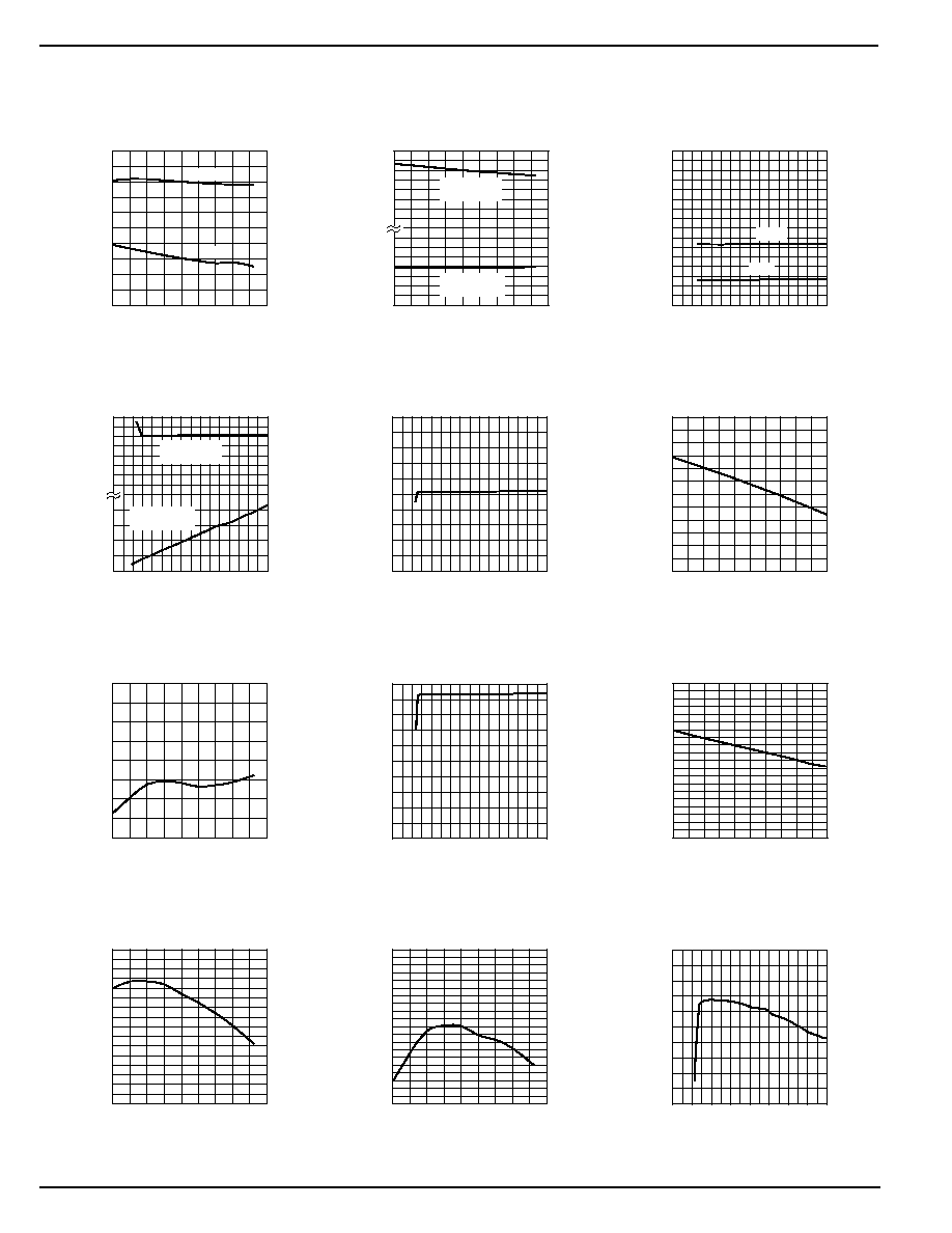
0
0.2
0.4
0.6
0.8
1.0
1.2
1.4
1.6
1.8
2.0
-40 -20 0 20 40 60 80 100120140
CURRENT (mA)
TEMPERATURE (
∞
C)
Quiescent Current
vs. Temperature
PWM
Skip
0
0.05
0.10
0.15
0.20
-40 -20 0 20 40 60 80 100120140
TEMPERATURE (
∞
C)
-0.50
0
0.50
1.00
1.50
Quiescent Current
vs. Temperature
UVLO Mode
(mA)
SHUTDOWN
(
µ
A)
CURRENT
(
mA
)
0
0.5
1.0
1.5
2.0
2.5
3.0
3.5
4.0
0
4
8
12 16 20 24 28 32
CURRENT (mA)
INPUT VOLTAGE (V)
Quiescent Current
vs. Supply Voltage
PWM
Skip
-0.5
0
0.5
1.0
1.5
0
0.1
0.2
0.3
0.4
0.5
0
4
8
12 16 20 24 28 32
SUPPLY VOLTAGE (V)
Quiescent Current
vs. Supply Voltage
UVLO Mode
(mA)
SHUTDOWN
(
µ
A)
CURRENT (
µ
A)
1.236
1.238
1.240
1.242
1.244
1.246
1.248
1.250
1.252
1.254
1.256
0
4
8
12 16 20 24 28 32
REFERENCE VOLTAGE (V)
SUPPLY VOLTAGE (V)
V
REF
(Fixed Versions)
Line Regulation
1.200
1.210
1.220
1.230
1.240
1.250
1.260
0
200
400
600
800
1000
REFERENCE VOLTAGE (V)
LOAD CURRENT (
µ
A)
V
REF
(Fixed Versions)
Load Regulation
1.240
1.245
1.250
1.255
1.260
-40 -20 0 20 40 60 80 100120140
REFERENCE VOLTAGE (V)
TEMPERATURE (
∞
C)
V
REF
(Fixed Versions)
vs. Temperature
4.0
4.2
4.4
4.6
4.8
5.0
0
4
8
12 16 20 24 28 32
V
DD
REGULATOR VOLTAGE (V)
SUPPLY VOLTAGE (V)
V
DD
Line Regulation
4.80
4.85
4.90
4.95
5.00
0
5
10
15
20
25
V
DD
REGULATOR VOLTAGE (V)
LOAD CURRENT (mA)
V
DD
Load Regulation
4.82
4.84
4.86
4.88
4.90
4.92
4.94
4.96
4.98
-40 -20 0 20 40 60 80 100120140
V
DD
REGULATOR VOLTAGE (V)
TEMPERATURE (
∞
C)
V
DD
vs. Temperature
-10
-8
-6
-4
-2
0
2
4
6
8
10
-40 -20 0 20 40 60 80 100120140
FREQUENCY VARIATION (%)
TEMPERATURE (
∞
C)
Oscillator Frequency
vs. Temperature
Typical Characteristics
-1.0
-0.8
-0.6
-0.4
-0.2
0
0.2
0.4
0.6
0.8
1.0
0
4
8
12 16 20 24 28 32
FREQUENCY VARIATION (%)
SUPPLY VOLTAGE (V)
Oscillator Frequency
vs. Supply Voltage
June 2000
7
MIC2182
MIC2182
Micrel
4.0
4.2
4.4
4.6
4.8
5.0
-40 -20 0 20 40 60 80 100120140
CURRENT (
µ
A)
TEMPERATURE (
∞
C)
Soft-Start Current
vs. Temperature
0.08
0.09
0.10
0.11
0.12
-40 -20 0 20 40 60 80 100120140
OVERCURRENT THRESHOLD (V)
TEMPERATURE (
∞
C)
Overcurrent Threshold
vs. Temperature
0
1
2
3
4
5
0
1
2
3
4
5
6
7
8
OUTPUT VOLTAGE (V)
OUTPUT CURRENT (A)
Current-Limit
Foldback
V
IN
= 5V
V
OUT
= 3.3V
R
CS
= 15m

MIC2182
Micrel
MIC2182
8
June 2000
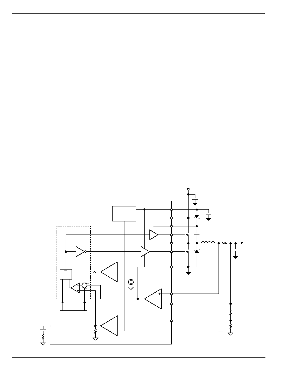
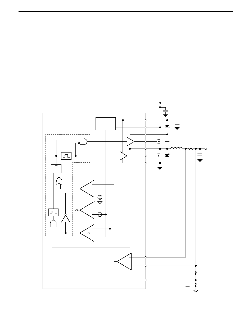
Block Diagrams
SGND
G
m
= 0.2
◊
10
-3
Low
Comp
Current
Limit
Skip-Mode
Current
Limit
PWM Mode
to Skip
Mode
Hysteresis
Comp
V
BG
1.245V
V
BG
0.07V
≠2%V
BG
Error
Amp
Control
Logic
V
IN
V
DD
PWM
PWM OUTPUT
CORRECTIVE
RAMP
RESET
Reference
Oscillator
0.024V
EN/UVLO
6
11
14
10
16
15
13
12
8
9
7
4
1
2
5
3
SS
PWM
SYNC
COMP
100k
MIC2182 [adj.]
FB
R2
R1
VOUT
CSH
VDD
VBST
C
IN
VIN
HSD
Q2
Q1
D1
D2
C
BST
C
OUT
V
IN
V
OUT
L1
VSW
LSD
PGND
C
COMP
R
COMP
4.7
µ
F
A
V
= 2
V
1.245V
R1
R2
OUT
=
+
1
V
6 V
OUT(max)
=
.0
Current
Sense
Amp
R
CS
Figure 2a. Adjustable Output Voltage Version

June 2000
9
MIC2182
MIC2182
Micrel
Low
Comp
Current
Limit
Skip-Mode
Current
Limit
Hysteresis
Comp
V
BG
1.245V
V
BG
0.07V
≠2%V
BG
Error
Amp
Control
Logic
V
IN
V
DD
PWM
PWM OUTPUT
CORRECTIVE
RAMP
RESET
Reference
Oscillator
0.024V
EN/UVLO
6
11
14
10
16
15
13
12
8
9
4
7
1
2
5
3
SS
PWM
SYNC
COMP
VREF
100k
G
m
= 0.2
◊
10
-3
MIC2182-x.x
SGND
R2
50k
R1*
VOUT
CSH
VDD
VBST
C
IN
VIN
HSD
Q2
Q1
D1
D2
C
BST
R
CS
C
OUT
V
IN
V
OUT
L1
VSW
LSD
PGND
C
COMP
R
COMP
4.7
µ
F
* 82.5k for 3.3V Output
150k for 5V Output
A
V
= 2
Current
Sense
Amp
PWM Mode
to Skip
Mode
Figure 2b. Fixed Output Voltage Versions
MIC2182
Micrel
MIC2182
10
June 2000
Functional Description
See "Applications Information" following this section for com-
ponent selection information and Figure 14 and Tables 1
through 5 for predesigned circuits.
The MIC2182 is a BiCMOS, switched-mode, synchronous
step-down (buck) converter controller. Current-mode control
is used to achieve superior transient line and load regulation.
An internal corrective ramp provides slope compensation for
stable operation above a 50% duty cycle. The controller is
optimized for high-efficiency, high-performance dc-dc con-
verter applications.
The MIC2182 block diagrams are shown in Figure 2a and
Figure 2b.
The MIC2182 controller is divided into 6 functions.
∑ Control loop
- PWM operation
- Skip-mode operation
∑ Current limit
∑ Reference, enable and UVLO
∑ MOSFET gate drive
∑ Oscillator and sync
∑ Soft start
Control Loop
PWM and Skip Modes of Operation
The MIC2182 operates in PWM (pulse-width-modulation)
mode at heavier output load conditions. At lighter load condi-
tions, the controller can be configured to automatically switch
to a pulse-skipping mode to improve efficiency. The potential
disadvantage of skip mode is the variable switching fre-
quency that accompanies this mode of operation. The occur-
rence of switching pulses depends on component values as
well as line and load conditions. There is an external sync
function that is disabled in skip mode. In PWM mode, the
synchronous buck converter forces continuous current to
flow in the inductor. In skip mode, current through the inductor
can settle to zero, causing voltage ringing across the induc-
tor. Pulling the PWM pin (pin 2) low will force the controller to
operate in PWM mode for all load conditions, which will
improve cross regulation of transformer coupled, multiple
output configurations.
PWM Control Loop
The MIC2182 uses current-mode control to regulate the
output voltage. This method senses the output voltage (outer
loop) and the inductor current (inner loop). It uses inductor
current and output voltage to determine the duty cycle of the
buck converter. Sampling the inductor current removes the
inductor from the control loop, which simplifies compensa-
tion.
Current
Sense
Amp
V
BG
1.245V
V
BG
Error
Amp
V
IN
V
DD
CORRECTIVE
RAMP
PWM
COMPARATOR
RESET
Reference
Oscillator
11
14
10
16
15
13
12
8
9
7
3
COMP
100k
MIC2182 [adj.] PWM Mode
FB
R2
R1
VOUT
CSH
VDD
VBST
C
IN
VIN
HSD
Q2
Q1
D1
D2
C
BST
C
OUT
V
IN
V
OUT
L1
VSW
LSD
PGND
C
COMP
R
COMP
4.7
µ
F
V
1.245V
R1
R2
OUT
=
+
1
S
R
Q
CONTROL LOGIC AND
PULSE-WIDTH MODULATOR
R
CS
G
m
= 0.2
◊
10
-3
A
V
= 2
0.024V
PWM Mode
to Skip
Mode
LOW
FORCES
SKIP MODE
Figure 3. PWM Operation
June 2000
11
MIC2182
MIC2182
Micrel
A block diagram of the MIC2182 PWM current-mode control
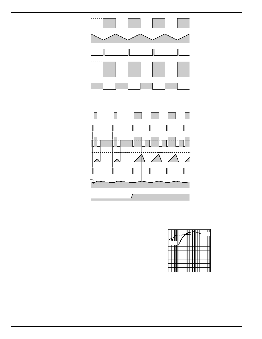
loop is shown in Figure 3 and the PWM mode voltage and
current waveforms are shown in figure 5A. The inductor
current is sensed by measuring the voltage across the
resistor, R
CS
. A ramp is added to the amplified current-sense
signal to provide slope compensation, which is required to
prevent unstable operation at duty cycles greater than 50%.
A transconductance amplifier is used for the error amplifier,
which compares an attenuated sample of the output voltage
with a reference voltage. The output of the error amplifier is
the COMP (compensation) pin, which is compared to the
current-sense waveform in the PWM block. When the current
signal becomes greater than the error signal, the comparator
turns off the high-side drive. The COMP pin (pin 3) provides
access to the output of the error amplifier and allows the use
of external components to stabilize the voltage loop.
Skip-Mode Control Loop
This control method is used to improve efficiency at light
output loads. At light output currents, the power drawn by the
MIC2182 is equal to the input voltage times the IC supply
current (I
Q
). At light output currents, the power dissipated by
the IC can be a significant portion of the total output power,
which lowers the efficiency of the power supply. The MIC2182
draws less supply current in skip mode by disabling portions
of the control and drive circuitry when the IC in not switching.
The disadvantage of this method is greater output voltage
ripple and variable switching frequency.
A block diagram of the MIC2182 skip mode is shown in Figure
4. Skip mode voltage and current waveforms are shown in
figure 5B.
Low
Comp
Skip-Mode
Current
Limit
V
BG
1.245V
V
BG
0.07V
LOW
FORCES
PWM MODE
≠2%V
BG
V
IN
V
DD
Reference
11
14
10
16
15
13
12
8
9
7
MIC2182 [adj.] Skip Mode
FB
R2
R1
VOUT
CSH
VDD
VBST
C
IN
VIN
HSD
Q2
Q1
D2
C
BST
C
OUT
V
IN
V
OUT
L1
VSW
LSD
PGND
4.7
µ
F
V
1.245V
R1
R2
OUT
=
+
1
Current
Sense
Amp
S
R
Q
CONTROL LOGIC AND
SKIP-MODE LOGIC
R
CS
A
V
= 2
ONE SHOT
LOW-SIDE DRIVER
ONE SHOT
Hysteresis
Comp
±
1%
Figure 4. Skip-Mode Operation
MIC2182
Micrel
MIC2182
12
June 2000
A hysteretic comparator is used in place of the PWM error
amplifier and a current-limit comparator senses the inductor
current. A one-shot starts the switching cycle by momentarily
turning on the low side MOSFET to insure the high side drive
boost capacitor, Cbst, is fully charged. The high side MOS-
FET is turned on and current ramps up in the inductor, L1.
The high side drive is turned off when either the peak voltage
on the input of the current-sense comparator exceeds the
threshold, typically 35mV, or the output voltage rises above
the hysteretic threshold of the output voltage comparator.
Once the high side MOSFET is turned off, the load current
discharges the output capacitor, causing V
OUT
to fall. The
cycle repeats when V
OUT
falls below the lower threshold, ≠
1%.
The maximum peak inductor current depends on the skip-
mode current-limit threshold and the value of the current-
sense resistor, R
CS
.
I
35mV
R
inductor(peak)
sense
=
Figure 6 shows the improvement in efficiency that skip mode
makes when at lower output currents.
0
20
40
60
80
100
0.01
0.1
1
10
100
EFFICIENCY (%)
OUTPUT CURRENT (A)
Skip
PWM
Figure 6. Efficiency
V
DD
0V
0V
0V
0V
0A
V
DD
V
IN
+ V
DD
V
IN
V
SW
Reset
Pulse
V
HSD
V
LSD
I
LOAD
I
L1
Figure 5a. PWM-Mode Timing
0V
0V
0V
0A
V
DD
+1%
≠1%
V
NOMINAL
V
IN
V
OUT
V
SW
V
LSD
V
HSD
V
one-shot
0V
V
DD
0V
V
DD
I
LIM(skip)
I
L1
V
OUT
I
OUT
0A
Figure 5b. Skip-Mode Timing
June 2000
13
MIC2182
MIC2182
Micrel
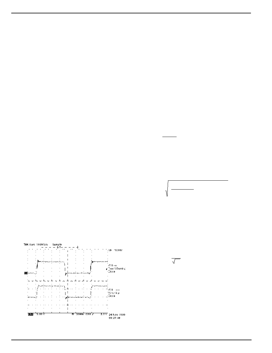
Switching from PWM to Skip Mode
The current sense amplifier in Figure 3 monitors the average
voltage across the current-sense resistor. The controller will
switch from PWM to skip mode when the average voltage
across the current-sense resistor drops below approximately
12mV. This is shown in Figure 7b. The average output current
at this transition level for is calculated below.
I
0.012
R
OUT(skipmode)
CS
=
where:
0.012 = threshold voltage of the internal comparator
R
CS
= current-sense resistor value
Switching from Skip to PWM Mode
The frequency of occurrence of the skip-mode current pulses
increase as the output current increases until the hysteretic
duty cycle reaches 100% (continuous pulses). Increasing the
current past this point will cause the output voltage will drop.
The low limit comparator senses the output voltage when it
drops below 2% of the set output and automatically switches
the converter to PWM mode.
The inductor current in skip mode is a triangular wave shape
a minimum value of 0 and a maximum value of 35mV/R
CS
(see Figure 7b). The maximum average output current in skip
mode is the average value of the inductor waveform:
I
0.5
35mV
R
OUT(max skipmode)
CS
=
◊
The capacitor on the PWM pin (pin 2) is discharged when the
IC transitions from skip to PWM mode. This forces the IC to
remain in PWM mode for a fixed period of time. The added
delay prevents unwanted switching between PWM and skip
mode. The capacitor is charged with a 10uA current source
on pin 2. The threshold on pin 2 is 2.5V. The delay for a typical
1nF capacitor is:
t
C
V
I
1nF
2.5V
10 A
250 s
delay
PWM
threshold
source
=
◊
=
◊
=
µ
µ
where:
C
PWM
= capacitor connected to pin 2
Current Limit
The current-limit circuit operates during PWM mode. The
output current is detected by the voltage drop across the
external current-sense resistor (R
CS
in Figure 2.). The cur-
rent-limit threshold is 100mV+35mV ≠25mV. The current-
sense resistor must be sized using the minimum current-limit
threshold. The external components must be designed to
withstand the maximum current limit. The current-sense
resistor value is calculated by the equation below:
R
75mV
I
CS
OUT(max)
=
The maximum output current is:
I
135mV
R
OUT(max)
CS
=
The current-sense pins CSH (pin 8) and V
OUT
(pin 9) are
noise sensitive due to the low signal level and high input
impedance. The PCB traces should be short and routed close
to each other. A small (1nF to 0.1
µ
F) capacitor across the pins
will attenuate high frequency switching noise.
When the peak inductor current exceeds the current-limit
threshold, the current-limit comparator, in Figure 2, turns off
the high-side MOSFET for the remainder of the cycle. The
output voltage drops as additional load current is pulled from
the converter. When the output voltage reaches approxi-
mately 0.95V, the circuit enters frequency-foldback mode
and the oscillator frequency will drop to 60kHz while maintain-
ing the peak inductor current equal to the nominal 100mV
across the external current-sense resistor. This limits the
maximum output power delivered to the load under a short
circuit condition.
Reference, Enable and, UVLO Circuits
The output drivers are enabled when the following conditions
are satisfied:
∑ The V
DD
voltage (pin 11) is greater than its
undervoltage threshold (typically 4.2V).
∑ The voltage on the enable pin is greater than the
enable UVLO threshold (typically 2.5V)
The internal bias circuit generates a 1.245V bandgap refer-
ence voltage for the voltage error amplifier and a 5V V
DD
voltage for the gate drive circuit. The reference voltage in the
fixed-output-voltage versions of the MIC2182 is buffered and
brought to pin 7. The V
REF
pin should be bypassed to GND
(pin 4) with a 0.1
µ
F capacitor. The adjustable version of the
MIC2182 uses pin 7 for output voltage sensing. A decoupling
capacitor on pin 7 is not used in the adjustable output voltage
version.
0A
I
LIM(skip)
Inductor
Current
35mV THRESHOLD
ACROSS R
CS
.
Figure 7a. Maximum Skip-Mode-Load Inductor Current
0A
I
MIN(PWM)
Inductor
Current
12mV THRESHOLD
OF AVERAGE VOLTAGE
ACROSS R
CS
.
Figure 7b. Minimum PWM-Mode-Load Inductor Current for PWM Operation
MIC2182
Micrel
MIC2182
14
June 2000
The enable pin (pin 6) has two threshold levels, allowing the
MIC2182 to shut down in a low current mode, or turn off output
switching in UVLO mode. An enable pin voltage lower than
the shutdown threshold turns off all the internal circuitry and
reduces the input current to typically 0.1
µ
A.
If the enable pin voltage is between the shutdown and UVLO
thresholds, the internal bias, V
DD
, and reference voltages are
turned on. The soft-start pin is forced low by an internal
discharge MOSFET. The output drivers are inhibited from
switching and remain in a low state. Raising the enable
voltage above the UVLO threshold of 2.5V allows the soft-
start capacitor to charge and enables the output drivers.
Either of two UVLO conditions will pull the soft-start capacitor
low.
∑ When the V
DD
drops below 4.1V
∑ When the enable pin drops below the 2.5V
threshold
MOSFET Gate Drive
The MIC2182 high-side drive circuit is designed to switch an
N-channel MOSFET. Referring to the block diagram in Figure
2, a bootstrap circuit, consisting of D2 and C
BST
, supplies
energy to the high-side drive circuit. Capacitor C
BST
is
charged while the low-side MOSFET is on and the voltage on
the V
SW
pin (pin 15) is approximately 0V. When the high-side
MOSFET driver is turned on, energy from C
BST
is used to turn
the MOSFET on. As the MOSFET turns on, the voltage on the
V
SW
pin increases to approximately V
IN
. Diode D2 is re-
versed biased and C
BST
floats high while continuing to keep
the high-side MOSFET on. When the low-side switch is
turned back on, C
BST
is recharged through D2.
The drive voltage is derived from the internal 5V V
DD
bias
supply. The nominal low-side gate drive voltage is 5V and the
nominal high-side gate drive voltage is approximately 4.5V
due the voltage drop across D2. A fixed 80ns delay between
the high- and low-side driver transitions is used to prevent
current from simultaneously flowing unimpeded through both
MOSFETs.
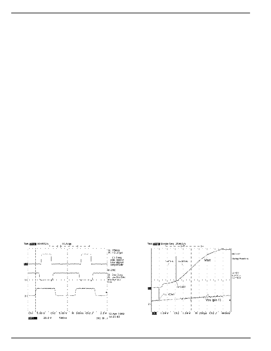
Oscillator and Sync
The internal oscillator is free running and requires no external
components. The nominal oscillator frequency is 300kHz. If
the output voltage is below approximately 0.95V, the oscilla-
tor operates in a frequency-foldback mode and the switching
frequency is reduced to 60kHz.
The SYNC input (pin 5) allows the MIC2182 to synchronize
with an external clock signal. The rising edge of the sync
signal generates a reset signal in the oscillator, which turns
off the low-side gate drive output. The high-side drive then
turns on, restarting the switching cycle. The sync signal is
inhibited when the controller operates in skip mode or during
frequency foldback. The sync signal frequency must be
greater than the maximum specified free running frequency
of the MIC2182. If the synchronizing frequency is lower,
double pulsing of the gate drive outputs will occur. When not
used, the sync pin must be connected to ground.
Figure 8 shows the timing between the external sync signal
(trace 2), the low-side drive (trace 1) and the high-side drive
(trace R1). There is a delay of approximately 250ns between
the rising edge of the external sync signal and turnoff of the
low-side MOSFET gate drive.
Some concerns of operating at higher frequencies are:
∑ Higher power dissipation in the internal V
DD
regulator. This occurs because the MOSFET
gates require charge to turn on the device. The
average current required by the MOSFET gate
increases with switching frequency. This in-
creases the power dissipated by the internal
V
DD
regulator. Figure 10 shows the total gate
charge which can be driven by the MIC2182
over the input voltage range, for different values
of switching frequency. The total gate charge
includes both the high- and low-side MOSFETs.
The larger SOP package is capable of dissipat-
ing more power than the SSOP package and
can drive larger MOSFETs with higher gate
drive requirements.
TIME
SYNC
SIGNAL
LO
W
-
SIDE
DRIVE
HIGH-SIDE
DRIVE
Figure 8. Sync Waveforms
TIME
V
SS
V
OUT
Figure 9. Startup Waveforms

June 2000
15
MIC2182
MIC2182
Micrel
∑ Reduced maximum duty cycle due to switching
transition times and constant delay times in the
controller. As the switching frequency increased,
the switching period decreases. The switching
transition times and constant delays in the
MIC2182 start to become noticeable. The effect
is to reduce the maximum duty cycle of the
controller. This will cause the minimum input to
output differential voltage (dropout voltage) to
increase.
0
20
40
60
80
100
0
4
8
12 16 20 24 28 32
GATE CHARGE (nC)
SUPPLY VOLTAGE (V)
400kHz
300kHz
500kHz
SOP
Figure 10a. SOP Gate Charge vs. Input Voltage
0
20
40
60
80
100
0
4
8
12 16 20 24 28 32
GATE CHARGE (nC)
SUPPLY VOLTAGE (V)
SSOP
400kHz
300kHz
500kHz
Figure 10b. SSOP Gate Charge vs. Input Voltage
It is recommended that the user limits the maximum synchro-
nized frequency to 600kHz. If a higher synchronized fre-
quency is required, it may be possible and will be design
dependent. Please consult Micrel applications for assis-
tance.
Soft Start
Soft start reduces the power supply input surge current at
startup by controlling the output voltage rise time. The input
surge appears while the output capacitance is charged up. A
slower output rise time will draw a lower input surge current.
Soft start may also be used for power supply sequencing.
The soft-start voltage is applied directly to the PWM compara-
tor. A 5uA internal current source is used to charge up the
soft-start capacitor. The capacitor is discharged when either
the enable voltage drops below the UVLO threshold (2.5V) or
the V
DD
voltage drops below the UVLO level (4.1V).
The part switches at a minimum duty cycle when the soft-start
pin voltage is less than 0.4V. This maintains a charge on the
bootstrap capacitor and insures high-side gate drive voltage.
As the soft-start voltage rises above 0.4V, the duty cycle
increases from the minimum duty cycle to the operating duty
cycle. The oscillator runs at the foldback frequency of 60kHz
until the output voltage rises above 0.95V. Above 0.95V, the
switching frequency increases to 300kHz (or the sync'd
frequency), causing the output voltage to rise a greater rate.
The rise time of the output is dependent on the soft-start
capacitor, output capacitance, output voltage, and load cur-
rent. The oscilloscope photo in Figure 9 show the output
voltage and the soft-start pin voltage at startup.
Minimum Pulse Width
The MIC2182 has a specified minimum pulse width. This
minimum pulse width places a lower limit on the minimum
duty cycle of the buck converter. When the MIC2182 is
operating in forced PWM mode (pin 2 low) and when the
output current is very low or zero, there is a limit on the ratio
of V
OUT
/V
IN
. If this limit is exceeded, the output voltage will
rise above the regulated voltage level. A minimum load is
required to prevent the output from rising up. This will not
occur for output voltages greater than 3V.
Figure 11 should be used as a guide when the MIC2182 is
forced into PWM-only mode. The actual maximum input
voltage will depend on the exact external components used
(MOSFETs, inductors, etc.).
10
15
20
25
30
35
0
1
2
3
4
5
6
INPUT VOLTAGE (V)
OUTPUT VOLTAGE (V)
Figure 11. Max. Input Voltage in Forced-PWM Mode
This restriction does not occur when the MIC2182 is set to
automatic mode (pin 2 connected to a capacitor) since the
converter operates in skip mode at low output current.

MIC2182
Micrel
MIC2182
16
June 2000
Applications Information
The following applications information includes component
selection and design guidelines. See Figure 14 and Tables 1
through 5 for predesigned circuits.
Inductor Selection
Values for inductance, peak, and RMS currents are required
to select the output inductor. The input and output voltages
and the inductance value determine the peak to peak inductor
ripple current. Generally, higher inductance values are used
with higher input voltages. Larger peak to peak ripple currents
will increase the power dissipation in the inductor and
MOSFETs. Larger output ripple currents will also require
more output capacitance to smooth out the larger ripple
current. Smaller peak to peak ripple currents require a larger
inductance value and therefore a larger and more expensive
inductor. A good compromise between size, loss and cost is
to set the inductor ripple current to be equal to 20% of the
maximum output current.
The inductance value is calculated by the equation below.
L
V
(V
V
)
V
f
0.2 I
OUT
IN(max)
OUT
IN(max)
S
OUT(max)
=
◊
-
◊ ◊
◊
where:
f
S
= switching frequency
0.2 = ratio of ac ripple current to dc output current
V
IN(max)
= maximum input voltage
The peak-to-peak inductor current (ac ripple current) is:
I
V
(V
V
)
V
f
L
PP
OUT
IN(max)
OUT
IN(max)
S
=
◊
-
◊ ◊
The peak inductor current is equal to the average output
current plus one half of the peak to peak inductor ripple
current.
I
I
0.5 I
PK
OUT(max)
PP
=
+
◊
The RMS inductor current is used to calculate the I
2
∑R losses
in the inductor.
I
(rms)
I
1
1
3
I
I
inductor
OUT(max)
PP
OUT(max)
2
=
◊
+
Maximizing efficiency requires the proper selection of core
material and minimizing the winding resistance. The high
frequency operation of the MIC2182 requires the use of ferrite
materials for all but the most cost sensitive applications.
Lower cost iron powder cores may be used but the increase
in core loss will reduce the efficiency of the power supply. This
is especially noticeable at low output power. The winding
resistance decreases efficiency at the higher output current
levels. The winding resistance must be minimized although
this usually comes at the expense of a larger inductor.
The power dissipated in the inductor is equal to the sum of the
core and copper losses. At higher output loads, the core
losses are usually insignificant and can be ignored. At lower
output currents, the core losses can be a significant contribu-
tor. Core loss information is usually available from the mag-
netics vendor.
Copper loss in the inductor is calculated by the equation
below:
P
I
(rms)
R
inductor Cu
inductor
2
winding
=
◊
The resistance of the copper wire, R
winding
, increases with
temperature. The value of the winding resistance used should
be at the operating temperature.
R
R
1 0.0042 (T
T
)
winding(hot)
winding(20 C)
hot
20 C
=
◊ +
◊
-
(
)
∞
∞
where:
T
HOT
= temperature of the wire
under operating load
T
20
∞
C
= ambient temperature
R
winding(20
∞
C)
is room temperature winding resistance
(usually specified by the manufacturer)
Current-Sense Resistor Selection
Low inductance power resistors, such as metal film resistors
should be used. Most resistor manufacturers make low
inductance resistors with low temperature coefficients, de-
signed specifically for current-sense applications. Both resis-
tance and power dissipation must be calculated before the
resistor is selected. The value of R
SENSE
is chosen based on
the maximum output current and the maximum threshold
level. The power dissipated is based on the maximum peak
output current at the minimum overcurrent threshold limit.
R
75mV
I
SENSE
OUT(max)
=
The maximum overcurrent threshold is:
I
135mV
R
overcurrent(max)
CS
=
The maximum power dissipated in the sense resistor is:
P
I
R
D(R
)
overcurrent(max)
2
CS
SENSE
=
◊
MOSFET Selection
External N-channel logic-level power MOSFETs must be
used for the high- and low-side switches. The MOSFET gate-
to-source drive voltage of the MIC2182 is regulated by an
internal 5V V
DD
regulator. Logic-level MOSFETs, whose
operation is specified at V
GS
= 4.5V must be used.
It is important to note the on-resistance of a MOSFET
increases with increasing temperature. A 75
∞
C rise in junc-
tion temperature will increase the channel resistance of the
MOSFET by 50% to 75% of the resistance specified at 25
∞
C.
This change in resistance must be accounted for when
calculating MOSFET power dissipation.
Total gate charge is the charge required to turn the MOSFET
on and off under specified operating conditions (V
DS
and
V
GS
). The gate charge is supplied by the MIC2182 gate drive
circuit. At 300kHz switching frequency and above, the gate

June 2000
17
MIC2182
MIC2182
Micrel
charge can be a significant source of power dissipation in the
MIC2182. At low output load this power dissipation is notice-
able as a reduction in efficiency. The average current re-
quired to drive the high-side MOSFET is:
I
Q
f
G[high-side](avg)
G
S
=
◊
where:
I
G[high-side](avg)
=
average high-side MOSFET gate current
Q
G
= total gate charge for the high-side MOSFET
taken from manufacturer's data sheet
with V
GS
= 5V.
The low-side MOSFET is turned on and off at V
DS
= 0
because the freewheeling diode is conducting during this
time. The switching losses for the low-side MOSFET is
usually negligable. Also, the gate drive current for the low-
side MOSFET is more accurately calculated using C
ISS
at
V
DS
= 0 instead of gate charge.
For the low-side MOSFET:
I
C
V
f
G[low-side](avg)
ISS
GS
S
=
◊
◊
Since the current from the gate drive comes from the input
voltage, the power dissipated in the MIC2182 due to gate
drive is:
P
V
I
I
gate drive
IN G[high-side](avg)
G[low-side](avg)
=
+
(
)
A convenient figure of merit for switching MOSFETs is the on-
resistance times the total gate charge (R
DS(on)
◊
Q
G
). Lower
numbers translate into higher efficiency. Low gate-charge
logic-level MOSFETs are a good choice for use with the
MIC2182. Power dissipation in the MIC2182 package limits
the maximum gate drive current. Refer to Figure 10 for the
MIC2182 gate drive limits.
Parameters that are important to MOSFET switch selection
are:
∑ Voltage rating
∑ On-resistance
∑ Total gate charge
The voltage rating of the MOSFETs are essentially equal to
the input voltage. A safety factor of 20% should be added to
the V
DS(max)
of the MOSFETs to account for voltage spikes
due to circuit parasitics.
The power dissipated in the switching transistor is the sum of
the conduction losses during the on-time (P
conduction
) and the
switching losses that occur during the period of time when the
MOSFETs turn on and off (P
AC
).
P
P
P
SW
conduction
AC
=
+
where:
P
I
(rms)
R
conduction
SW
2
SW
=
◊
P
P
P
AC
AC(off)
AC(on)
=
+
R
SW
= on-resistance of the MOSFET switch.
Making the assumption the turn-on and turnoff transition
times are equal, the transition time can be approximated by:
t
C
V
C
V
I
T
ISS
GS
OSS
IN
G
=
◊
+
◊
where:
C
ISS
and C
OSS
are measured at V
DS
= 0.
I
G
= gate drive current (1A for the MIC2182)
The total high-side MOSFET switching loss is:
P
(V
V ) I
t
f
AC
IN
D
PK
T
S
=
+
◊
◊
◊
where:
t
T
= switching transition time
(typically 20ns to 50ns)
V
D
= freewheeling diode drop, typically 0.5V.
f
S
it the switching frequency, nominally 300kHz
The low-side MOSFET switching losses are negligible and
can be ignored for these calculations.
RMS Current and MOSFET Power Dissipation Calculation
Under normal operation, the high-side MOSFET's RMS
current is greatest when V
IN
is low (maximum duty cycle). The
low-side MOSFET's RMS current is greatest when V
IN
is high
(minimum duty cycle). However, the maximum stress the
MOSFETs see occurs during short circuit conditions, where
the output current is equal to I
overcurrent(max)
. (See the Sense
Resistor section). The calculations below are for normal
operation. To calculate the stress under short circuit condi-
tions, substitute I
overcurrent(max)
for I
OUT(max)
. Use the formula
below to calculate D under short circuit conditions.
D
0.063 1.8 10
V
short circuit
3
IN
=
-
◊
◊
-
The RMS value of the high-side switch current is:
I
(rms)
D
I
I
12
SW(highside)
OUT(max)
2
PP
2
=
◊
+
I
(rms)
1 D I
I
12
SW(low side)
OUT(max)
2
PP
2
=
-
(
)
+
where:
D = duty cycle of the converter
D
V
V
OUT
IN
=
◊
= efficiency of the converter.
Converter efficiency depends on component parameters,
which have not yet been selected. For design purposes, an
efficiency of 90% can be used for V
IN
less than 10V and 85%
can be used for V
IN
greater than 10V. The efficiency can be
more accurately calculated once the design is complete. If the
assumed efficiency is grossly inaccurate, a second iteration
through the design procedure can be made.
For the high-side switch, the maximum dc power dissipation
is:
P
R
I
(rms)
switch1(dc)
DS(on)1
SW1
2
=
◊
MIC2182
Micrel
MIC2182
18
June 2000
For the low-side switch (N-channel MOSFET), the dc power
dissipation is:
P
R
I
(rms)
switch2(dc)
DS(on)2
SW 2
2
=
◊
Since the ac switching losses for the low side MOSFET is
near zero, the total power dissipation is:
P
P
low-side MOSFET(max)
switch2(dc)
=
The total power dissipation for the high side MOSFET is:
P
P
P
highsideMOSFET(max)
SWITCH 1(dc)
AC
=
+
External Schottky Diode
An external freewheeling diode is used to keep the inductor
current flow continuous while both MOSFETs are turned off.
This dead time prevents current from flowing unimpeded
through both MOSFETs and is typically 80ns The diode
conducts twice during each switching cycle. Although the
average current through this diode is small, the diode must be
able to handle the peak current.
I
I
2
80ns
f
D(avg)
OUT
S
=
◊ ◊
◊
The reverse voltage requirement of the diode is:
V
(rrm)
V
diode
IN
=
The power dissipated by the Schottky diode is:
P
I
V
diode
D(avg)
F
=
◊
where:
V
F
= forward voltage at the peak diode current
The external Schottky diode, D2, is not necessary for circuit
operation since the low-side MOSFET contains a parasitic
body diode. The external diode will improve efficiency and
decrease high frequency noise. If the MOSFET body diode is
used, it must be rated to handle the peak and average current.
The body diode has a relatively slow reverse recovery time
and a relatively high forward voltage drop. The power lost in
the diode is proportional to the forward voltage drop of the
diode. As the high-side MOSFET starts to turn on, the body
diode becomes a short circuit for the reverse recovery period,
dissipating additional power. The diode recovery and the
circuit inductance will cause ringing during the high-side
MOSFET turn-on.
An external Schottky diode conducts at a lower forward
voltage preventing the body diode in the MOSFET from
turning on. The lower forward voltage drop dissipates less
power than the body diode. The lack of a reverse recovery
mechanism in a Schottky diode causes less ringing and less
power loss. Depending on the circuit components and oper-
ating conditions, an external Schottky diode will give a 1/2%
to 1% improvement in efficiency. Figure 12 illustrates the
difference in noise on the VSW pin with and without a
Schottky diode.
Output Capacitor Selection
The output capacitor values are usually determined by the
capacitors ESR (equivalent series resistance). Voltage rating
and RMS current capability are two other important factors in
selecting the output capacitor. Recommended capacitors are
tantalum, low-ESR aluminum electrolytics, and OS-CON.
The output capacitor's ESR is usually the main cause of
output ripple. The maximum value of ESR is calculated by:
R
V
I
ESR
OUT
PP
where:
V
OUT
= peak to peak output voltage ripple
I
PP
= peak to peak inductor ripple current
The total output ripple is a combination of the ESR and the
output capacitance. The total ripple is calculated below:
V
I
(1 D)
C
f
I
R
OUT
PP
OUT
S
2
PP
ESR
2
=
◊ -
◊
+
◊
(
)
where:
D = duty cycle
C
OUT
= output capacitance value
f
S
= switching frequency
The voltage rating of capacitor should be twice the output
voltage for a tantalum and 20% greater for an aluminum
electrolytic or OS-CON.
The output capacitor RMS current is calculated below:
I
(rms)
I
12
C
PP
OUT
=
The power dissipated in the output capacitor is:
P
I
(rms)
R
DISS(C
C
2
ESR(C
)
OUT
OUT
OUT
)
=
◊
Input Capacitor Selection
The input capacitor should be selected for ripple current
rating and voltage rating. Tantalum input capacitors may fail
when subjected to high inrush currents, caused by turning the
input supply on. Tantalum input capacitor voltage rating
should be at least 2 times the maximum input voltage to
maximize reliability. Aluminum electrolytic, OS-CON, and
multilayer polymer film capacitors can handle the higher
inrush currents without voltage derating.
TIME
WITH
FREEWHEELING DIODE
WITHOUT
FREEWHEELING DIODE
Figure 12. Switch Output Noise
With and Without Shottky Diode

June 2000
19
MIC2182
MIC2182
Micrel
The input voltage ripple will primarily depend on the input
capacitors ESR. The peak input current is equal to the peak
inductor current, so:
V
I
R
IN
inductor(peak)
ESR(C )
IN
=
◊
The input capacitor must be rated for the input current ripple.
The RMS value of input capacitor current is determined at the
maximum output current. Assuming the peak to peak induc-
tor ripple current is low:
I
(rms)
I
D (1 D)
C
OUT(max)
IN
◊
◊ -
The power dissipated in the input capacitor is:
P
I
(rms)
R
DISS(C )
C
2
ESR(C )
IN
IN
IN
=
◊
Voltage Setting Components
The MIC2182-3.3 and MIC2182-5.0 ICs contain internal
voltage dividers that set the output voltage. The MIC2182
adjustable version requires two resistors to set the output
voltage as shown in Figure 13.
Error
Amp
7
MIC2182 [adj.]
FB
V
REF
1.245V
R2
R1
Figure 13. Voltage-Divider Configuration
The output voltage is determined by the equation:
V
V
1
R1
R2
O
REF
=
◊ +
Where: V
REF
for the MIC2182 is typically 1.245V.
A typical value of R1 can be between 3k and 10k. If R1 is too
large it may allow noise to be introduced into the voltage
feedback loop. If R1 is too small in value it will decrease the
efficiency of the power supply, especially at low output loads.
Once R1 is selected, R2 can be calculated using:
R2
V
R1
V
V
REF
O
REF
=
◊
-
Voltage Divider Power Dissipation
The reference voltage and R2 set the current through the
voltage divider.
I
V
R2
divider
REF
=
The power dissipated by the divider resistors is:
P
(R1 R2) I
divider
divider
2
=
+
◊
Efficiency Calculation and Considerations
Efficiency is the ratio of output power to input power. The
difference is dissipated as heat in the buck converter. Under
light output load, the significant contributors are:
∑ Supply current to the MIC2182
∑ MOSFET gate-charge power (included in the IC
supply current)
∑ Core losses in the output inductor
To maximize efficiency at light loads:
∑ Use a low gate-charge MOSFET or use the
smallest MOSFET, which is still adequate for
maximum output current.
∑ Allow the MIC2182 to run in skip mode at lower
currents.
∑ Use a ferrite material for the inductor core, which
has less core loss than an MPP or iron power
core.
Under heavy output loads the significant contributors to
power loss are (in approximate order of magnitude):
∑ Resistive on-time losses in the MOSFETs
∑ Switching transition losses in the MOSFETs
∑ Inductor resistive losses
∑ Current-sense resistor losses
∑ Input capacitor resistive losses (due to the
capacitors ESR)
To minimize power loss under heavy loads:
∑ Use logic-level, low on-resistance MOSFETs.
Multiplying the gate charge by the on-resistance
gives a Figure of merit, providing a good bal-
ance between low and high load efficiency.
∑ Slow transition times and oscillations on the
voltage and current waveforms dissipate more
power during turn-on and turnoff of the
MOSFETs. A clean layout will minimize parasitic
inductance and capacitance in the gate drive
and high current paths. This will allow the fastest
transition times and waveforms without oscilla-
tions. Low gate-charge MOSFETs will transition
faster than those with higher gate-charge
requirements.
∑ For the same size inductor, a lower value will
have fewer turns and therefore, lower winding
resistance. However, using too small of a value
will require more output capacitors to filter the
output ripple, which will force a smaller band-
width, slower transient response and possible
instability under certain conditions.
∑ Lowering the current-sense resistor value will
decrease the power dissipated in the resistor.
However, it will also increase the overcurrent
limit and will require larger MOSFETs and
inductor components.
∑ Use low-ESR input capacitors to minimize the
power dissipated in the capacitors ESR.
Decoupling Capacitor Selection
The 4.7
µ
F decoupling capacitor is used to minimize noise on
the VDD pin. The placement of this capacitor is critical to the
proper operation of the IC. It must be placed right next to the

MIC2182
Micrel
MIC2182
20
June 2000
pins and routed with a wide trace. The capacitor should be a
good quality tantalum. An additional 1
µ
F ceramic capacitor
may be necessary when driving large MOSFETs with high
gate capacitance. Incorrect placement of the V
DD
decoupling
capacitor will cause jitter or oscillations in the switching
waveform and large variations in the overcurrent limit.
A 0.1
µ
F ceramic capacitor is required to decouple the VIN.
The capacitor should be placed near the IC and connected
directly to between pin 10 (Vcc) and pin 12 (PGND).
PCB Layout and Checklist
PCB layout is critical to achieve reliable, stable and efficient
performance. A ground plane is required to control EMI and
minimize the inductance in power, signal and return paths.
The following guidelines should be followed to insure proper
operation of the circuit.
∑ Signal and power grounds should be kept
separate and connected at only one location.
Large currents or high di/dt signals that occur
when the MOSFETs turn on and off must be
kept away from the small signal connections.
∑ The connection between the current-sense
resistor and the MIC2182 current-sense inputs
(pin 8 and 9) should have separate traces,
routed from the terminals directly to the IC pins.
The traces should be routed as closely as
possible to each other and their length should be
minimized. Avoid running the traces under the
inductor and other switching components. A 1nF
to 0.1
µ
F capacitor placed between pins 8 and 9
will help attenuate switching noise on the current
sense traces. This capacitor should be placed
close to pins 8 and 9.
∑ When the high-side MOSFET is switched on, the
critical flow of current is from the input capacitor
through the MOSFET, inductor, sense resistor,
output capacitor, and back to the input capacitor.
These paths must be made with short, wide
pieces of trace. It is good practice to locate the
ground terminals of the input and output capaci-
tors close to each.
∑ When the low-side MOSFET is switched on,
current flows through the inductor, sense
resistor, output capacitor, and MOSFET. The
source of the low-side MOSFET should be
located close to the output capacitor.
∑ The freewheeling diode, D1 in Figure 2, con-
ducts current during the dead time, when both
MOSFETs are off. The anode of the diode
should be located close to the output capacitor
ground terminal and the cathode should be
located close to the input side of the inductor.
∑ The 4.7
µ
F capacitor, which connects to the VDD
terminal (pin 11) must be located right at the IC.
The VDD terminal is very noise sensitive and
placement of this capacitor is very critical.
Connections must be made with wide trace. The
capacitor may be located on the bottom layer of
the board and connected to the IC with multiple
vias.
∑ The V
IN
bypass capacitor should be located
close to the IC and connected between pins 10
and 12. Connections should be made with a
ground and power plane or with short, wide
trace.
June 2000
21
MIC2182
MIC2182
Micrel
VDD
BST
C6
0.1
µ
F
R1
2k
R7
100k
V
IN
V
OUT
GND
C2
2.2nF
C4
1nF
C3
0.1
µ
F
C5
0.1
µ
F
C1
0.1
µ
F
50V
C9
4.7
µ
F
16V
C11
(table)
D2
SD103BWS
Q2
(table)
D1
(table)
C7
(table)
C12
0.1
µ
F
50V
L1
(table)
R2
(table)
Q1
(table)
HSD
VSW
LSD
PGND
CSH
VOUT
VREF
SGND
GND
MIC2182
VIN
EN/UVLO
SS
PWM
COMP
SYNC
C13, 1nF
Figure 14. Basic Circuit Diagram for Use with Tables 3 through 6
n
o
i
t
a
c
i
f
i
c
e
p
S
t
i
m
i
L
e
l
p
p
i
r
y
c
n
e
u
q
e
r
f
g
n
i
h
c
t
i
w
S
e
g
a
t
l
o
v
t
u
p
t
u
o
f
o
%
1
e
r
u
t
a
r
e
p
m
e
t
t
n
e
i
b
m
a
m
u
m
i
x
a
M
5
8
∞
C
y
t
il
i
b
a
p
a
c
t
i
u
c
r
i
c
-
t
r
o
h
S
s
u
o
u
n
i
t
n
o
C
y
c
n
e
u
q
e
r
f
g
n
i
h
c
t
i
w
S
z
H
k
0
0
3
Table 1. Specifications for Figure 14 and Tables 3 through 6
Manufacturer
Telephone Number (USA)
Web Address
AVX
(803) 946-0690
www.avxcorp.com
Central Semiconductor
(516) 435-1110
www.centralsemi.com
Coiltronics
(561) 241-7876
www.coiltronics.com
IRC
(704) 264-8861
IR
(310) 322-3331
www.irf.com
Micrel
(408) 944-0800
www.micrel.com
Vishay/Lite On
(805) 446-4800
www.vishay-liteon.com
(diodes)
Vishay/Siliconix
(800) 554-5665
www.siliconix.com
(MOSFETs)
Vishay/Dale
(800) 487-9437
www.vishaytechno.com
(inductors and resistors)
Sumida
(847) 956-0666
www.japanlink.com/sumida
Table 2. Component Suppliers
Predesigned Circuits
A single schematic diagram, shown in Figure 14, can be used
to build power supplies ranging from 3A to 10A at the common
output voltages of 1.8V, 2.5V, 3.3V, and 5V. Components that
vary, depending upon output current and voltage, are listed
in the accompanying Tables 3 through 6.
Power supplies larger than 10A can also be constructed
using the MIC2182 using larger power-handling compo-
nents.
The "Power Supply Operating Characteristics" graphs follow-
ing the component and vendor tables provide useful informa-
tion about the actual performance of some of these circuits.

MIC2182
Micrel
MIC2182
22
June 2000
3A (6.5V≠30V)
4A (6.5V≠30V)
5A (6.5V≠30V)
10A (6.5V≠10V)
Reference
Part No. / Description
Part No. / Description
Part No. / Description
Part No. / Description
C7
qty: 2
qty: 2
qty: 2
qty: 2
TPSE227M010R0100
TPSE227M010R0100
TPSV227M010R0060
TPSV337M010R0060
AVX, 220
µ
F 10V,
AVX, 220
µ
F 10V,
AVX, 220
µ
F 10V,
AVX, 330
µ
F 10V,
0.1
ESR,
0.1
ESR,
0.06
ESR,
0.06
ESR,
output filter capacitor
output filter capacitor
output filter capacitor
output filter capacitor
C11
qty: 2
qty: 3
qty: 4
qty: 4
TPSE226M035R0300
TPSE226M035R0300
TPSE226M035R0300
TPSV107M020R0085
AVX, 22
µ
F 35V,
AVX, 22
µ
F 35V,
AVX, 22
µ
F 35V,
AVX, 100
µ
F 20V,
0.3
ESR,
0.3
ESR,
0.3
ESR,
0.06
ESR,
input filter capacitor
input filter capacitor
input filter capacitor
input filter capacitor
D1
qty: 1 B140, Vishay,
qty: 1 B140, Vishay,
qty: 1 B140, Vishay,
qty: 1 B330, Vishay,
freewheeling diode
freewheeling diode
freewheeling diode
freewheeling diode
L1
qty: 1 CDRH125-100,
qty: 1 CDRH127-100,
qty: 1 CDRH127-100
qty: 1 UP4B-3R3,
Sumida Inductor,
Sumida Inductor,
Sumida,
Coiltronics,
10
µ
H 4A,
10
µ
H 5A,
10
µ
H 5A,
3.3
µ
H 11A,
output inductor
output inductor
output inductor
output inductor
Q1
qty: 1 Si4800, Siliconix,
qty: 1 Si4800, Siliconix,
qty: 1 Si4884, Siliconix,
qty: 2 Si4884, Siliconix
low-side MOSFET
low-side MOSFET
low-side MOSFET
low-side MOSFET
Q2
qty: 1 Si4800, Siliconix,
qty: 1 Si4800, Siliconix,
qty: 1 Si4884, Siliconix,
qty: 2 Si4884, Siliconix,
high-side MOSFET
high-side MOSFET
high-side MOSFET
high-side MOSFET
R2
qty: 1
qty: 1
qty: 1
qty: 2
WSL-2010 .025 1%,
WSL-2010 .020 1%,
WSL-2512 .015 1%,
WSL-2512 .015 1% ,
Vishay, 0.025, 1%, 0.5W,
Vishay, 0.02, 1%, 0.5W,
Vishay, 0.015, 1%, 1W,
Vishay, 0.015, 1%, 1W,
current sense resistor
current sense resistor
current sense resistor
current sense resistor
U1
MIC2182-5.0BSM or
MIC2182-5.0BSM or
MIC2182-5.0BSM or
MIC2182-5.0BM
MIC2182-5.0BM
MIC2182-5.0BM
MIC2182-5.0BM
Table 3. Components for 5V Output
3A (4.5V≠30V)
4A (4.5V≠30V)
5A (4.5V≠30V)
10A (4.5V≠5.5V)
Reference
Part No. / Description
Part No. / Description
Part No. / Description
Part No. / Description
C7
qty: 2
qty: 2
qty: 2
qty: 2
TPSE227M010R0100
TPSE227M010R0100
TPSV227M010R0060
TPSV477M006R0055
AVX, 220
µ
F 10V,
AVX, 220
µ
F 10V,
AVX, 220
µ
F 10V,
AVX, 470
µ
F 6.3V,
0.1
ESR,
0.1
ESR,
0.06
ESR,
0.055
ESR,
output filter capacitor
output filter capacitor
output filter capacitor
output filter capacitor
C11
qty: 2
qty: 2
qty: 3
qty: 3
TPSE226M035R0300
TPSE226M035R0300
TPSE226M035R0300
TPSV227M016R0075
AVX, 22
µ
F 35V,
AVX, 22
µ
F 35V,
AVX, 22
µ
F 35V,
AVX, 220
µ
F 16V,
0.3
ESR,
0.3
ESR,
0.3
ESR,
0.075
ESR,
input filter capacitor
input filter capacitor
input filter capacitor
filter capacitor
D1
qty: 1 B140, Vishay,
qty: 1 B140, Vishay,
qty: 1 B140, Vishay,
qty: 1 B330, Vishay,
freewheeling diode
freewheeling diode
freewheeling diode
freewheeling diode
L1
qty: 1 CDRH125-100,
qty: 1 CDRH127-100,
qty: 1 CDRH127-100
qty: 1 UP4B-3R3,
Sumida Inductor,
Sumida Inductor,
Sumida,
Coiltronics,
10
µ
H 4A,
10
µ
H 5A,
10
µ
H 5A,
3.3
µ
H 11A,
output inductor
output inductor
output inductor
output inductor
Q1
qty: 1 Si4800, Siliconix,
qty: 1 Si4800, Siliconix,
qty: 1 Si4800, Siliconix,
qty: 2 Si4884, Siliconix,
low-side MOSFET
low-side MOSFET
low-side MOSFET
low-side MOSFET
Q2
qty: 1 Si4800, Siliconix,
qty: 1 Si4800, Siliconix,
qty: 1 Si4884, Siliconix,
qty: 2 Si4884, Siliconix,
high-side MOSFET
high-side MOSFET
high-side MOSFET
high-side MOSFET
R2
qty: 1
qty: 1
qty: 1
qty: 2
WSL-2010 .025 1%,
WSL-2010 .020 1%,
WSL-2512 .015 1%,
WSL-2512 .015 1% ,
Vishay, 0.025, 1%, 0.5W,
Vishay, 0.02, 1%, 0.5W,
Vishay, 0.015, 1%, 1W,
Vishay, 0.015, 1%, 1W,
current sense resistor
current sense resistor
current sense resistor
current sense resistor
U1
MIC2182-3.3BSM or
MIC2182-3.3BM or
MIC2182-3.3BM or
MIC2182-3.3BM
MIC2182-3.3BM
MIC2182-3.3BSM
MIC2182-3.3BSM
Table 4. Components for 3.3V Output

June 2000
23
MIC2182
MIC2182
Micrel
3A (4.5V≠30V)
4A (4.5V≠30V)
5A (4.5V≠30V)
10A (4.5V≠5.5V)
Reference
Part No. / Description
Part No. / Description
Part No. / Description
Part No. / Description
C7
qty: 2
qty: 2
qty: 2
qty: 2
TPSE227M010R0100
TPSE227M010R0100
TPSV227M010R0060
TPSV447M006R0055
AVX, 220
µ
F 10V,
AVX, 220
µ
F 10V,
AVX, 220
µ
F 10V,
AVX, 470
µ
F 6.3V,
0.1
ESR,
0.1
ESR,
0.06
ESR,
0.06
ESR,
output filter capacitor
output filter capacitor
output filter capacitor
output filter capacitor
C11
qty: 2
qty: 2
qty: 2
qty: 3
TPSE226M035R0300
TPSE226M035R0300
TPSE226M035R0300
TPSV227M016R0075
AVX, 22
µ
F 35V,
AVX, 22
µ
F 35V,
AVX, 22
µ
F 35V,
AVX, 220
µ
F 16V,
0.3
ESR,
0.3
ESR,
0.3
ESR,
0.06
ESR,
input filter capacitor
input filter capacitor
input filter capacitor
input filter capacitor
D1
qty: 1 B140, Vishay,
qty: 1 B140, Vishay,
qty: 1 B140, Vishay,
qty: 1 B330, Vishay,
freewheeling diode
freewheeling diode
freewheeling diode
freewheeling diode
L1
qty: 1 CDRH125-100,
qty: 1 CDRH127-100,
qty: 1 CDRH127-100
qty: 1 UP4B-3R3,
Sumida Inductor,
Sumida Inductor,
Sumida,
Coiltronics,
10
µ
H 4A,
10
µ
H 5A,
10
µ
H 5A,
3.3
µ
H 11A,
output inductor
output inductor
output inductor
output inductor
Q1
qty: 1 Si4800, Siliconix,
qty: 1 Si4884, Siliconix,
qty: 1 Si4884, Siliconix,
qty: 2 Si4884, Siliconix
low-side MOSFET
low-side MOSFET
low-side MOSFET
low-side MOSFET
Q2
qty: 1 Si4800, Siliconix,
qty: 1 Si4800, Siliconix,
qty: 1 Si4800, Siliconix,
qty: 2 Si4884, Siliconix,
high-side MOSFET
high-side MOSFET
high-side MOSFET
high-side MOSFET
R2
qty: 1
qty: 1
qty: 1
qty: 1
WSL-2010 .025 1%,
WSL-2010 .020 1%,
WSL-2512 .015 1%,
WSL-2512 .015 1% ,
Vishay, 0.025, 1%, 0.5W,
Vishay, 0.02, 1%, 0.5W,
Vishay, 0.015, 1%, 1W,
Vishay, 0.015, 1%, 1W,
current sense resistor
current sense resistor
current sense resistor
current sense resistor
U1
MIC2182BSM or
MIC2182BSM or
MIC2182BSM or
MIC2182BM
MIC2182BM
MIC2182BM
MIC2182BM
Table 5. Components for 2.5V Output
3A (4.5V≠30V)
4A (4.5V≠30V)
5A (4.5V≠8V)
10A (4.5V≠5.5V)
Reference
Part No. / Description
Part No. / Description
Part No. / Description
Part No. / Description
C7
qty: 2
qty: 2
qty: 2
qty: 2
TPSE227M010R0100
TPSE227M010R0100
TPSV227M010R0060
TPSV447M006R0055
AVX, 220
µ
F 10V,
AVX, 220
µ
F 10V,
AVX, 220
µ
F 10V,
AVX, 470
µ
F 6.3V,
0.1
ESR,
0.1
ESR,
0.06
ESR,
0.06
ESR,
output filter capacitor
output filter capacitor
output filter capacitor
output filter capacitor
C11
qty: 2
qty: 2
qty: 2
qty: 2
TPSE226M035R0300
TPSE226M035R0300
TPSE226M035R0300
TPSV227M016R0075
AVX, 22
µ
F 35V,
AVX, 22
µ
F 35V,
AVX, 22
µ
F 35V,
AVX, 220
µ
F 16V,
0.3
ESR,
0.3
ESR,
0.3
ESR,
0.06
ESR,
input filter capacitor
input filter capacitor
input filter capacitor
input filter capacitor
D1
qty: 1 B140, Vishay,
qty: 1 B140, Vishay,
qty: 1 B140, Vishay,
qty: 1 B330, Vishay,
freewheeling diode
freewheeling diode
freewheeling diode
freewheeling diode
L1
qty: 1 CDRH125-100,
qty: 1 CDRH127-100,
qty: 1 CDRH127-100
qty: 1 UP4B-3R3,
Sumida Inductor,
Sumida Inductor,
Sumida,
Coiltronics,
10
µ
H 4A,
10
µ
H 5A,
10
µ
H 5A,
3.3
µ
H 11A,
output inductor
output inductor
output inductor
output inductor
Q1
qty: 1 Si4800, Siliconix,
qty: 1 Si4884, Siliconix,
qty: 1 Si4884, Siliconix,
qty: 2 Si4884, Siliconix
low-side MOSFET
low-side MOSFET
low-side MOSFET
low-side MOSFET
Q2
qty: 1 Si4800, Siliconix,
qty: 1 Si4800, Siliconix,
qty: 1 Si4800, Siliconix,
qty: 2 Si4884, Siliconix,
high-side MOSFET
high-side MOSFET
high-side MOSFET
high-side MOSFET
R2
qty: 1
qty: 1
qty: 1
qty: 2
WSL-2010 .025 1%,
WSL-2010 .020 1%,
WSL-2512 .015 1%,
WSL-2512 .015 1% ,
Vishay, 0.025, 1%, 0.5W,
Vishay, 0.02, 1%, 0.5W,
Vishay, 0.015, 1%, 1W,
Vishay, 0.015, 1%, 1W,
current sense resistor
current sense resistor
current sense resistor
current sense resistor
U1
MIC2182BSM or
MIC2182BSM or
MIC2182BSM or
MIC2182BM
MIC2182BM
MIC2182BM
MIC2182BM
Table 6. Components for 1.8V Output

MIC2182
Micrel
MIC2182
24
June 2000
Effect of Soft-Start Capacitor (C
SS
) Value
On Output Voltage Waveforms
During Turn-On
(10A Power Supply Configuration)
Effect of Soft-Start Capacitor (C
SS
) Value
On Output Voltage Waveforms
During Turn-On
(4A Power Supply Configuration)
Normal (300kHz Switching Frequency) and
Output Short-Circuit (60kHz) Conditions
Switch Node (Pin 15) Waveforms
Converter Waveforms
QTY: 2
Si4884
HIGH-SIDE
MOSFETS
SWITCH-NODE
VOLTAGE
INDUCTOR CURRENT
LOW-SIDE MOSFET
GATE-TO-SOURCE VOLTAGE
HIGH-SIDE MOSFET
GATE-TO-SOURCE VOLTAGE
QTY: 2
Si4884
LOW-SIDE
MOSFETS
V
IN
= 7V
L1 = 3.3
µ
H
V
OUT
= 3.3V
I
OUT
= 10A
V
SW
PIN 15
V
SW+HSD
PIN 16
V
GS
LO
W
-
SIDE
MOSFET
V
GS
HIGH-SIDE
MOSFET
I
L1
(2A/div)
HIGH-SIDE
DRIVE VOLTAGE
REFERENCED TO GROUND
10Amps
Typical Skip-Mode Waveforms
V
OUT
V
SW
Pin 15
I
L1
(0.5A/div)
Typical PWM-Mode Waveforms
V
OUT
V
SW
Pin 15
I
L1
(0.5A/div)
Power Supply Operating Characteristics

June 2000
25
MIC2182
MIC2182
Micrel
-40
-20
0
20
40
60
80
100
0
30
60
90
120
150
180
210
10x10
0
100x10
0
1x10
3
10x10
3
100x10
3
300x10
3
GAIN (dB)
PHASE (
∞
)
FREQUENCY (Hz)
Bode Plot
(4A Power Supply Configuration)
GAIN
PHASE
Load Transient Response
and Bode Plot
(4A Power Supply Configuration)
V
IN
= 12V
V
OUT
= 3.3V
L1 = 10
µ
H
R2 = 20m
I
OUT
2A/div
V
OUT
Load Transient Response
and Bode Plot
(10A Power Supply Configuration)
V
IN
= 6V
V
OUT
= 3.3V
L1 = 3.3
µ
H
R2 = 7.5m
I
OUT
5A/div
V
OUT
-40
-20
0
20
40
60
80
100
0
30
60
90
120
150
180
210
10x10
0
100x10
0
1x10
3
10x10
3
100x10
3
300x10
3
GAIN (dB)
PHASE (
∞
)
FREQUENCY (Hz)
Bode Plot
(10A Power Supply Configuration)
GAIN
PHASE
0
20
40
60
80
100
0.01
0.1
1
10
EFFICIENCY (%)
OUTPUT CURRENT (A)
Skip
PWM
R2 = 7.5m
L1 = 3.3
µ
H
2 high-side MOSFETs: Si4884
2 low-side MOSFETs: Si4884
Efficiency
(10A Power Supply Configuration)
0
20
40
60
80
100
0.01
0.1
1
4
EFFICIENCY (%)
OUTPUT CURRENT (A)
Skip
PWM
V
IN
= 5V
R2 = 15m
L1 = 10
µ
H
1 high-side MOSFET: Si4800
1 low-side MOSFET: Si4800
5V Efficiency
(4A Power Supply Configuration)
0
20
40
60
80
100
0.01
0.1
1
4
EFFICIENCY (%)
OUTPUT CURRENT (A)
12V Efficiency
(4A Power Supply Configuration)
Skip
PWM
V
IN
= 12V
R2 = 15m
L1 = 10
µ
H
1 high-side MOSFET: Si4800
1 low-side MOSFET: Si4800
0
20
40
60
80
100
0.01
0.1
1
4
EFFICIENCY (%)
OUTPUT CURRENT (A)
Skip
PWM
V
IN
= 24V
R2 = 15m
L1 = 10
µ
H
1 high-side MOSFET: Si4800
1 low-side MOSFET: Si4800
24V Efficiency
(4A Power Supply Configuration)

MIC2182
Micrel
MIC2182
26
June 2000
Package Information
45
∞
0
∞
≠8
∞
0.244 (6.20)
0.228 (5.79)
0.394 (10.00)
0.386 (9.80)
SEATING
PLANE
0.020 (0.51)
REF
0.020 (0.51)
0.013 (0.33)
0.157 (3.99)
0.150 (3.81)
0.050 (1.27)
0.016 (0.40)
0.0648 (1.646)
0.0434 (1.102)
0.050 (1.27)
BSC
PIN 1
DIMENSIONS:
INCHES (MM)
0.0098 (0.249)
0.0040 (0.102)
16-pin SOP (M)
2.00 (0.079)
1.73 (0.068)
0.21 (0.008)
0.05 (0.002)
COPLANARITY:
0.10 (0.004) MAX
1.25 (0.049) REF
0.65 (0.0260)
BSC
0.875
(0.034) REF
10
∞
4
∞
0
∞
≠8
∞
5.40 (0.213)
5.20 (0.205)
7.90 (0.311)
7.65 (0.301)
6.33 (0.239)
6.07 (0.249)
0.38 (0.015)
0.25 (0.010)
0.22 (0.009)
0.13 (0.005)
0.95 (0.037)
0.55 (0.022)
DIMENSIONS:
MM (INCH)
16-Pin SSOP (SM)

June 2000
27
MIC2182
MIC2182
Micrel

MIC2182
Micrel
MIC2182
28
June 2000
MICREL INC.
1849 FORTUNE DRIVE
SAN JOSE, CA 95131
USA
TEL
+ 1 (408) 944-0800
FAX
+ 1 (408) 944-0970
WEB
http://www.micrel.com
This information is believed to be accurate and reliable, however no responsibility is assumed by Micrel for its use nor for any infringement of patents or
other rights of third parties resulting from its use. No license is granted by implication or otherwise under any patent or patent right of Micrel Inc.
© 2000 Micrel Incorporated