May 2004
1
M9999-052104
MIC2202
Micrel
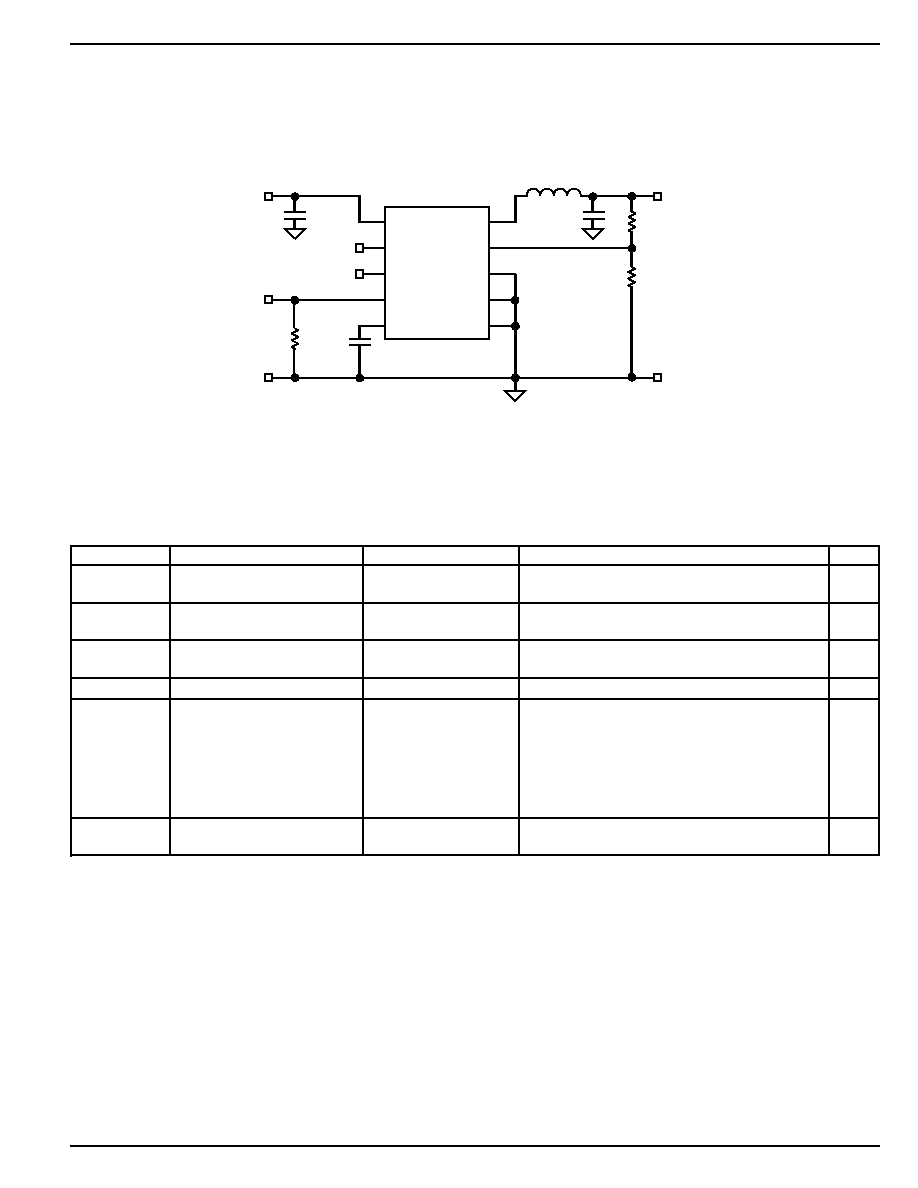
Typical Application
MIC2202
High Efficiency 2MHz Synchronous Buck
Converter 1
µ
F Stable PWM Regulator
General Description
The Micrel MIC2202 is a high efficiency 2MHz PWM synchro-
nous buck regulator. The fast 2MHz operation along with a
proprietary compensation scheme allows the smallest pos-
sible external components. The MIC2202 can operate with
a 1
µ
F ceramic output capacitor and a small, low DC-resis-
tance, 2.2
µ
H inductor, reducing system size and cost while
allowing a high level of efficiency.
The MIC2202 operates from 2.3V to 5.5V input and features
internal power MOSFETs that can supply over 600mA of
output current with output voltages down to 0.5V. The
MIC2202 implements a constant 2MHz pulse- width-modu-
lation (PWM) control scheme which reduces noise in sensi-
tive RF, audio, and communications applications. Addition-
ally, the MIC2202 can be synchronized to an external clock,
or multiple MIC2202s can easily be daisy-chained with the
SYNCLOCK feature.
The MIC2202 has a high bandwidth loop (up to 500kHz)
which allows ultra fast transient response times. This is very
useful when powering applications that require fast dynamic
response such as CPU cores and RF circuitry in high
performance cellular phones and PDAs.
The MIC2202 is available in 10-pin MSOP and 3mm
◊
3mm
MLFTM-10L package options with an operating junction
temperature range from ≠40
∞
C to +125
∞
C .
Features
∑ Input voltage range: 2.3V to 5.5V
∑ Output down to 0.5V/600mA
∑ 2MHz PWM operation
∑ Stable with 1
µ
F ceramic output capcitor.
∑ Ultra-fast transient response (up to 500kHz GBW)
∑ Internal compensation
∑ All ceramic capacitors
∑ >95% efficiency
∑ Fully integrated MOSFET switches
∑ Easily synchronized to external clock
∑ SYNCLOCK feature to daisy chain multiple 2202s
∑ Requires only 4 external components
∑ 1% line and load regulation
∑ Logic controlled micropower shutdown
∑ Thermal shutdown and current limit protection
∑ 10-pin MSOP and 3mm
◊
3mm MLFTM-10L package
options
∑ ≠40
∞
C to +125
∞
C junction temperature range
Applications
∑ Cellular phones
∑ PDAs
∑ 802.11 WLAN power supplies
∑ FPGA/ASIC power supplies
∑ Dynamically adjustable power supply for CDMA/W-
CDMA RF power amps
∑ DSL modems
∑ Tape drives
10nF
2.2
µ
H
V
OUT
3.3V
600mA
V
IN
2.3V to 5.5V
1
µ
F
10k
1.78k
EN
6
5
1
SYNC_IN
SYNC_OUT
10
9
8
7
2
3
4
Adjustable Output Synchronous Buck Converter
Micrel, Inc. ∑ 1849 Fortune Drive ∑ San Jose, CA 95131 ∑ USA ∑ tel + 1 (408) 944-0800 ∑ fax + 1 (408) 474-1000 ∑ http://www.micrel.com
Micro
LeadFrame and MLF are trademarks of Amkor Technology, Inc.
60
65
70
75
80
85
90
95
100
0
0.1
0.2
0.3
0.4
0.5
0.6
EFFICIENCY (%)
OUTPUT CURRENT (A)
Efficiency 3.3V
OUT
5V
IN
4.2V
IN
L = 2.2
µ
H
C
OUT
= 1
µ
F

MIC2202
Micrel
M9999-052104
2
May 2004
EN
FB
6
5
1
SW
VIN
SYNC_IN
SYNC_OUT
10 GND
GND
GND
BIAS
9
8
7
2
3
4
Pin Configuration
Pin Description
Pin Number
Pin Name
Pin Function
1
SW
Switch (Output): Internal power MOSFET output switches.
2
VIN
Supply Voltage (Input): Requires bypass capacitor to GND.
3
SYNC_IN
SYNC_IN for the MIC2202: Sync the main switching frequency to an
external clock.
4
SYNC_OUT
SYNC_OUT an open collector output.
5
EN
A low level EN will power down the device, reducing the quiescent current to
under 1
µ
A.
6
FB
Input to the error amplifier, connect to the external resistor divider network to
set the output voltage.
7
BIAS
Internal circuit bias supply, nominally 2.3V. Must be de-coupled to signal
ground with a 0.01
µ
F capacitor.
8, 9, 10
GND
Ground.
EP
GND
Ground, backside pad.
SW
VIN
SYNC_IN
SYNC_OUT
GND
GND
GND
BIAS
1
2
3
4
10
9
8
7
5
6
EN
FB
EP
MSOP-10 (MM)
MLFTM-10 (ML)
(Top View)
Ordering Information
Part Number
Voltage
Temperature Range
Package
Lead Finish
MIC2202BMM
Adjustable
≠40
∞
C to +125
∞
C
10-pin MSOP-10
Standard
MIC2202BML
Adjustable
≠40
∞
C to +125
∞
C
10-pin MLFTM
Standard
MIC2202YMM
Adjustable
≠40
∞
C to +125
∞
C
10-pin MSOP-10
Pb-Free
MIC2202YML
Adjustable
≠40
∞
C to +125
∞
C
10-pin MLFTM
Pb-Free

May 2004
3
M9999-052104
MIC2202
Micrel
Absolute Maximum Ratings
(Note 1)
Supply Voltage (V
IN
) ....................................................... 6V
Output Switch Voltage (V
SW
) .......................................... 6V
Logic Input Voltage (V
EN
, V
SYNC_IN
) ............... V
IN
to ≠0.3V
Power Dissipation .................................................... Note 3
Storage Temperature (T
S
) ....................... ≠65
∞
C to +150
∞
C
ESD Rating (Note 4) ..................................................... 2kV
Operating Ratings
(Note 2)
Supply Voltage (V
IN
) ................................... +2.3V to +5.5V
Junction Temperature (T
J
) ................ ≠40
∞
C
T
J
+125
∞
C
Package Thermal Resistance
MSOP-10L (
JA
) ................................................ 115
∞
C/W
3mm
◊
3mm MLFTM-10L (
JA
) ............................... 60
∞
C/W
Electrical Characteristics
(Note 5)
T
A
= 25
∞
C with V
IN
= 3.5V unless otherwise noted, bold values indicate ≠40
∞
C < T
J
< +125
∞
C
Parameter
Condition
Min
Typ
Max
Units
Supply Voltage Range
2.3
5.5
V
Quiescent Current
EN = V
IN
; V
FB
= 0.55V (not switching)
350
450
µ
A
EN = 0V
0.01
1
µ
A
MIC2202 [Adjustable] Feedback
0.4875
0.500
0.5125
V
Voltage
Output Voltage Line Regulation
V
OUT
< 2V; V
IN
= 2.3V to 5.5V, I
LOAD
= 100mA
0.05
0.5
%
Output Voltage Load Regulation
0mA < I
LOAD
< 500mA
0.1
0.5
%
Bias Regulator Output Voltage
2.2
2.32
2.6
V
Maximum Duty Cycle
V
FB
= 0.7V
100
%
Current Limit
V
FB
= 0.7V
1
1.8
2.5
A
Switch ON-Resistance
V
IN
= 3.5V, I
SW
= 300mA V
FB
= 0.35V
0.650
0.9
V
IN
= 3.5V, I
SW
= ≠300mA V
FB
= 0.55V
0.550
0.75
Enable Input Current
0.01
1
µ
A
Sync Frequency Range
1.6
2.5
MHz
SYNC_IN Threshold
0.7
1
1.7
V
Sync Minimum Pulse Width
10
ns
SYNC_IN Input Current
1
µ
A
Oscillator Frequency
1.8
2
2.2
MHz
Enable Threshold
0.5
0.9
1.3
V
Enable Hysteresis
20
mV
Over-temperature Shutdown
160
∞
C
Over-temperature Shutdown
20
∞
C
Hysteresis
Note 1.
Exceeding the ABSOLUTE MAXIMUM RATINGS may damage device.
Note 2.
The device is not guaranteed to function outside its operating rating.
Note 3.
Absolute maximum power dissipation is limited by maximum junction temperature where P
D(MAX)
= (T
J(MAX)
≠T
A
)
˜
JA
.
Note 4.
Devices are ESD sensitive. Handling precautions recommended. Human body model, 1.5k in series with 100pF.
Note 5.
Specification for packaged product only.

MIC2202
Micrel
M9999-052104
4
May 2004
Typical Characteristics
0.4950
0.4975
0.5000
0.5025
0.5050
0
0.1
0.2
0.3
0.4
0.5
OUTPUT VOLTAGE (V)
OUTPUT CURRENT (A)
Output Voltage
vs. Output Current
0.485
0.490
0.495
0.500
0.505
0.510
0.515
-40 -20 0
20 40 60 80 100 120
OUTPUT VOLTAGE (V)
TEMPERATURE (
∞
C)
Output Voltage
vs. Temperature
0
0.5
1.0
1.5
2.0
2.5
0
2
4
6
V
BIAS
(V)
SUPPLY VOLTAGE (V)
V
BIAS
vs. Supply Voltage
V
FB
= 0V
2.302
2.304
2.306
2.308
2.31
2.312
2.314
2.316
2.318
2.320
-40 -20 0
20 40 60 80 100 120
BIAS SUPPLY (V)
TEMPERATURE (
∞
C)
Bias Supply
vs. Temperature
0
50
100
150
200
250
300
350
0
1
2
3
4
5
6
I
Q
(µA)
SUPPLY VOLTAGE (V)
Quiescent Current
vs. Supply Voltage
V
FB
= 0V
332
334
336
338
340
342
344
346
348
350
352
354
-40 -20 0
20 40 60 80 100 120
I
Q
(µA)
TEMPERATURE (
∞
C)
Quiescent Current
vs. Temperature
V
IN
= 3.6V
1.60
1.70
1.80
1.90
2.00
2.10
2.20
2.30
2.40
-40 -20 0
20 40 60 80 100 120
FREQUENCY (MHz)
TEMPERATURE (
∞
C)
Frequency
vs. Temperature
0
0.1
0.2
0.3
0.4
0.5
0.6
0.7
0.8
0.9
1.0
2.3 2.8 3.3 3.8 4.3 4.8 5.3
ENABLE THRESHOLD (V)
SUPPLY VOLTAGE (V)
Enable Threshold
vs. Supply Voltage
Enable On
Enable Off
0
0.1
0.2
0.3
0.4
0.5
0.6
0.7
0.8
0.9
-40 -20 0
20 40 60 80 100 120
ENABLE THRESHOLD (V)
TEMPERATURE (
∞
C)
Enable Threshold
vs. Temperature
3.6V
IN

May 2004
5
M9999-052104
MIC2202
Micrel
Block Diagram
Error
Amplifier
SW
C
OUT
V
OUT
FB
EN
BIAS
SYNC_IN
SYNC_OUT
PGND
PWM
Comparator
0.5V
MIC2202
Internal
Supply
Oscillator
Ramp
Generator
V
IN
C
IN
VIN
Driver
MIC2202 Block Diagram

MIC2202
Micrel
M9999-052104
6
May 2004
Functional Description
V
IN
V
IN
provides power to the output and to the internal bias
supply. The supply voltage range is from 2.3V to 5.5V. A
minimum 1
µ
F ceramic is recommended for bypassing the
input supply.
Enable
The enable pin provides a logic level control of the output. In
the off state, supply current of the device is greatly reduced
(typically <1
µ
A). Also, in the off state, the output drive is
placed in a "tri-stated" condition, where both the high side
P-Channel MOSFET and the low-side N-Channel are in an off
or non-conducting state. Do not drive the enable pin above
the supply voltage.
Sync_In
Sync_In pin enables the ability to change the fundamental
switching frequency. The Sync_In frequency has a minimum
frequency of 1.6MHz and a maximum sync frequency of
2.5MHz.
Careful attention should be paid to not driving the Sync_In pin
greater than the supply voltage. While this will not damage
the device, it can cause improper operation.
Sync_Out
Sync_Out is an open collector output that provides a signal
equal to the internal oscillator frequency. This creates the
ability for multiple MIC2202s to be connected together in a
master-slave configuration for frequency matching of the
converters. A typical 10k
is recommended for a pull-up
resistor.
Bias
The bias supply is an internal 2.3V linear regulator that
supplies the internal biasing voltage to the MIC2202. A 10nF
ceramic capacitor is required on this pin for bypassing. Do not
use the bias pin as a supply. The bias pin was designed to
supply internal power only.
Feedback
The feedback pin provides the control path to control the
output. A resistor divider connecting the feedback to the
output is used to adjust the desired output voltage. Refer to
the feedback section in the
"Applications Information"
for
more detail.
10k
SYNC_IN
VIN
MIC2202
"Master"
SYNC_OUT
SW
BIAS
FB
SYNC_IN
VIN
MIC2202
"Slave"
SYNC_OUT
SW
BIAS
FB
Figure 1. Master-Slave Operation

May 2004
7
M9999-052104
MIC2202
Micrel
Applications Information
Input Capacitor
A minimum 1
µ
F ceramic is recommended on the V
IN
pin for
bypassing. X5R or X7R dielectrics are recommended for the
input capacitor. Y5V dielectrics, aside from losing most of
their capacitance over temperature, they also become resis-
tive at high frequencies. This reduces their ability to filter out
high frequency noise.
Output Capacitor
The MIC2202 was designed specifically for the use of a 1
µ
F
ceramic output capacitor. This value can be increased to
improve transient performance. Since the MIC2202 is volt-
age mode, the control loop relies on the inductor and output
capacitor for compensation. For this reason, do not use
excessively large output capacitors. The output capacitor
requires either an X7R or X5R dielectric. Y5V and Z5U
dielectric capacitors, aside from the undesirable effect of their
wide variation in capacitance over temperature, become
resistive at high frequencies. Using Y5V or Z5U capacitors
will cause instability in the MIC2202.
Total output capacitance should not exceed 15
µ
F. Large
values of capacitance can cause current limit to engage
during start-up. If larger than 15
µ
F is required, a feed-forward
capacitor from the output to the feedback node should be
used to slow the start up time.
Inductor Selection
Inductor selection will be determined by the following (not
necessarily in the order of importance):
∑ Inductance
∑ Rated current value
∑ Size requirements
∑ DC resistance (DCR)
The MIC2202 is designed for use with a 1
µ
H to 4.7
µ
H
inductor.
Maximum current ratings of the inductor are generally given
in two methods: permissible DC current and saturation cur-
rent. Permissible DC current can be rated either for a 40
∞
C
temperature rise or a 10% loss in inductance. Ensure the
inductor selected can handle the maximum operating cur-
rent. When saturation current is specified, make sure that
there is enough margin that the peak current will not saturate
the inductor.
The size requirements refer to the area and height require-
ments that are necessary to fit a particular design. Please
refer to the inductor dimensions on their datasheet.
DC resistance is also important. While DCR is inversely
proportional to size, DCR can represent a significant effi-
ciency loss. Refer to the
"Efficiency Considerations"
below
for a more detailed description.
Bias Capacitor
A small 10nF ceramic capacitor is required to bypass the bias
pin. The use of low ESR ceramics provides improved filtering
for the bias supply.
Efficiency Considerations
Efficiency is defined as the amount of useful output power,
divided by the amount of power consumed.
Efficiency %
V
I
V
I
100
OUT
OUT
IN
IN
=
◊
◊
◊
Maintaining high efficiency serves two purposes. It reduces
power dissipation in the power supply, reducing the need for
heat sinks and thermal design considerations and it reduces
consumption of current for battery powered applications.
Reduced current draw from a battery increases the devices
operating time, critical in hand held devices.
There are two loss terms in switching converters: DC losses
and switching losses. DC losses are simply the power dissi-
pation of I
2
R. Power is dissipated in the high side switch
during the on cycle. Power loss is equal to the high side
MOSFET RDS
(ON)
multiplied by the Switch Current
2
. During
the off cycle, the low side N-Channel MOSFET conducts, also
dissipating power. Device operating current also reduces
efficiency. The product of the quiescent (operating) current
and the supply voltage is another DC loss. The current
required to drive the gates on and off at a constant 2MHz
frequency and the switching transitions make up the switch-
ing losses.
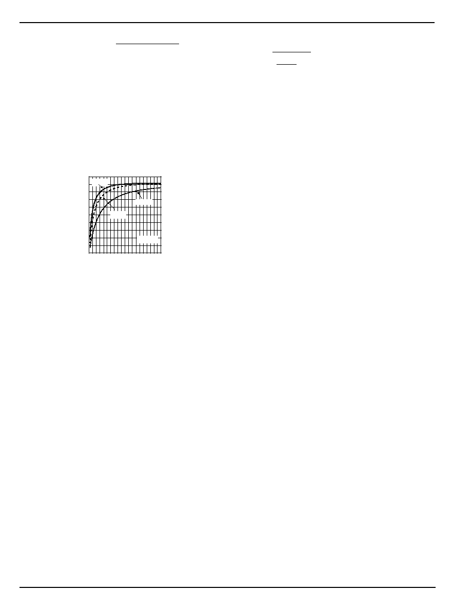
Figure 2 shows an efficiency curve. The non-shaded portion,
from 0mA to 200mA, efficiency losses are dominated by
quiescent current losses, gate drive and transition losses. In
this case, lower supply voltages yield greater efficiency in that
they require less current to drive the MOSFETs and have
reduced input power consumption.
50
55
60
65
70
75
80
85
90
95
100
0
0.1
0.2
0.3
0.4
0.5
0.6
EFFICIENCY (%)
OUTPUT CURRENT (A)
3.3V
OUT
4.2V
IN
5V
IN
Efficiency
vs. Output Current
Figure 2. Efficiency Curve
The shaded region, 200mA to 500mA, efficiency loss is
dominated by MOSFET RDS
(ON)
and inductor DC losses.
Higher input supply voltages will increase the Gate-to-Source
threshold on the internal MOSFETs, reducing the internal
RDS
(ON)
. This improves efficiency by reducing DC losses in
the device. All but the inductor losses are inherent to the
device. In which case, inductor selection becomes increas-
ingly critical in efficiency calculations. As the inductors are
reduced in size, the DC resistance (DCR) can become quite
significant. The DCR losses can be calculated as follows;
L
I
DCR
PD
OUT
=
◊
2
From that, the loss in efficiency due to inductor resistance can
be calculated as follows:

MIC2202
Micrel
M9999-052104
8
May 2004
Efficiency Loss
1≠
V
I
V
I
L
100
OUT
OUT
OUT
OUT
PD
=
◊
◊
+
◊
Efficiency loss due to DCR is minimal at light loads and gains
significance as the load is increased. Inductor selection
becomes a trade-off between efficiency and size in this case.
Alternatively, under lighter loads, the ripple current due to the
inductance becomes a significant factor. When light load
efficiencies become more critical, a larger inductor value may
be desired. Larger inductances reduce the peak-to-peak
ripple current which minimize losses. The following graph
illustrates the effects of inductance value at light load.
0
20
40
60
80
100
0
25
50
75
100
EFFICIENCY (%)
OUTPUT CURRENT (mA)
1.8V
OUT
4.7
µ
H
1
µ
H
Efficiency
vs. Inductance
2.2
µ
H
Figure 3. Efficiency vs. Inductance
Compensation
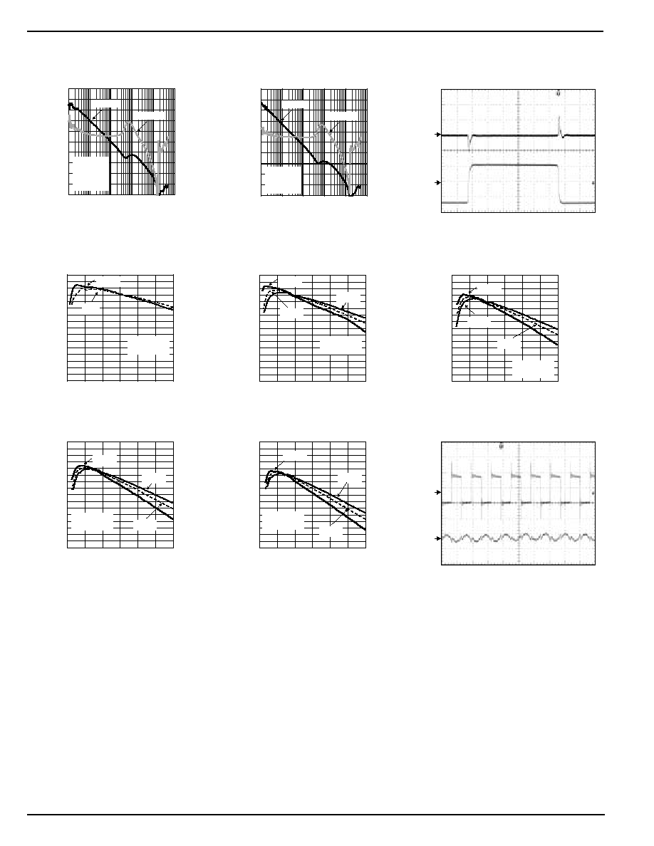
The MIC2202 is an internally compensated, voltage mode
buck regulator. Voltage mode is achieved by creating an
internal 2MHz ramp signal and using the output of the error
amplifier to pulse width modulate the switch node, maintain-
ing output voltage regulation. With a typical gain bandwidth of
200kHz, the MIC2202 is capable of extremely fast transient
responses.
The MIC2202 is designed to be stable with a 2.2
µ
H inductor
and a 1
µ
F ceramic (X5R) output capacitor. These values can
be interchanged (i.e. 1
µ
H inductor and a 2.2
µ
F capacitor).
The trade off between changing these values is that with a
larger inductor, there is a reduced peak-to-peak current
which yields a greater efficiency at lighter loads. A larger
output capacitor will improve transient response by providing
a larger hold up reservoir of energy to the output.
Feedback
The MIC2202 provides a feedback pin to adjust the output
voltage to the desired level. This pin connects internally to an
error amplifier. The error amplifier then compares the voltage
at the feedback to the internal 0.5V reference voltage and
adjusts the output voltage to maintain regulation. To calculate
the resistor divider network for the desired output is as
follows:
R2
R1
V
V
≠ 1
OUT
REF
=
Where V
REF
is 0.5V and V
OUT
is the desired output voltage.
A 10k
or lower resistor value from the output to the feedback
is recommended. Larger resistor values require an additional
capacitor (feed-forward) from the output to the feedback. The
large high side resistor value and the parasitic capacitance on
the feedback pin (~10pF) can cause an additional pole in the
loop. The additional pole can create a phase loss at high
frequency. This phase loss degrades transient response by
reducing phase margin. Adding feed-forward capacitance
negates the parasitic capacitive effects of the feedback pin.
A minimum 1000pF capacitor is recommended for feed-
forward capacitance.
Also, large feedback resistor values increase the impedance,
making the feedback node more susceptible to noise pick-up.
A feed-forward capacitor would also reduce noise pick-up by
providing a low impedance path to the output.
PWM Operation
The MIC2202 is a pulse width modulation (PWM) controller.
By controlling the ratio of on-to-off time, or duty cycle, a
regulated DC output voltage is achieved. As load or supply
voltage changes, so does the duty cycle to maintain a
constant output voltage. In cases where the input supply runs
into a dropout condition, the MIC2202 will run at 100% duty
cycle.
The MIC2202 provides constant switching at 2MHz with
synchronous internal MOSFETs. The internal MOSFETs
include a high-side P-Channel MOSFET from the input
supply to the switch pin and an N-Channel MOSFET from the
switch pin to ground. Since the low-side N-Channel MOSFET
provides the current during the off cycle, a free wheeling
Schottky diode from the switch node to ground is not required.
PWM control provides fixed frequency operation. By main-
taining a constant switching frequency, predictable funda-
mental and harmonic frequencies are achieved. Other meth-
ods of regulation, such as burst and skip modes, have
frequency spectrums that change with load that can interfere
with sensitive communication equipment.

May 2004
9
M9999-052104
MIC2202
Micrel
Synchronization
Sync_In allows the user to change the frequency from 2MHz
up to 2.5MHz or down to 1.6MHz. This allows the ability to
control the fundamental frequency and all the resultant har-
monics. Maintaining a predictable frequency creates the
ability to either shift the harmonics away from sensitive carrier
and IF frequency bands or to accurately filter out specific
harmonic frequencies.
10k
SYNC_IN
VIN
MIC2202
"Master"
SYNC_OUT
SW
BIAS
FB
SYNC_IN
VIN
MIC2202
"Slave"
SYNC_OUT
SW
BIAS
FB
Figure 4. Master-Slave Operation
TIME (400ns/div.)
Sla
v
e
Switch Mode
Master
Sync Out
Master
Switch Mode
Figure 5. Master-Slave Synchronization Waveforms
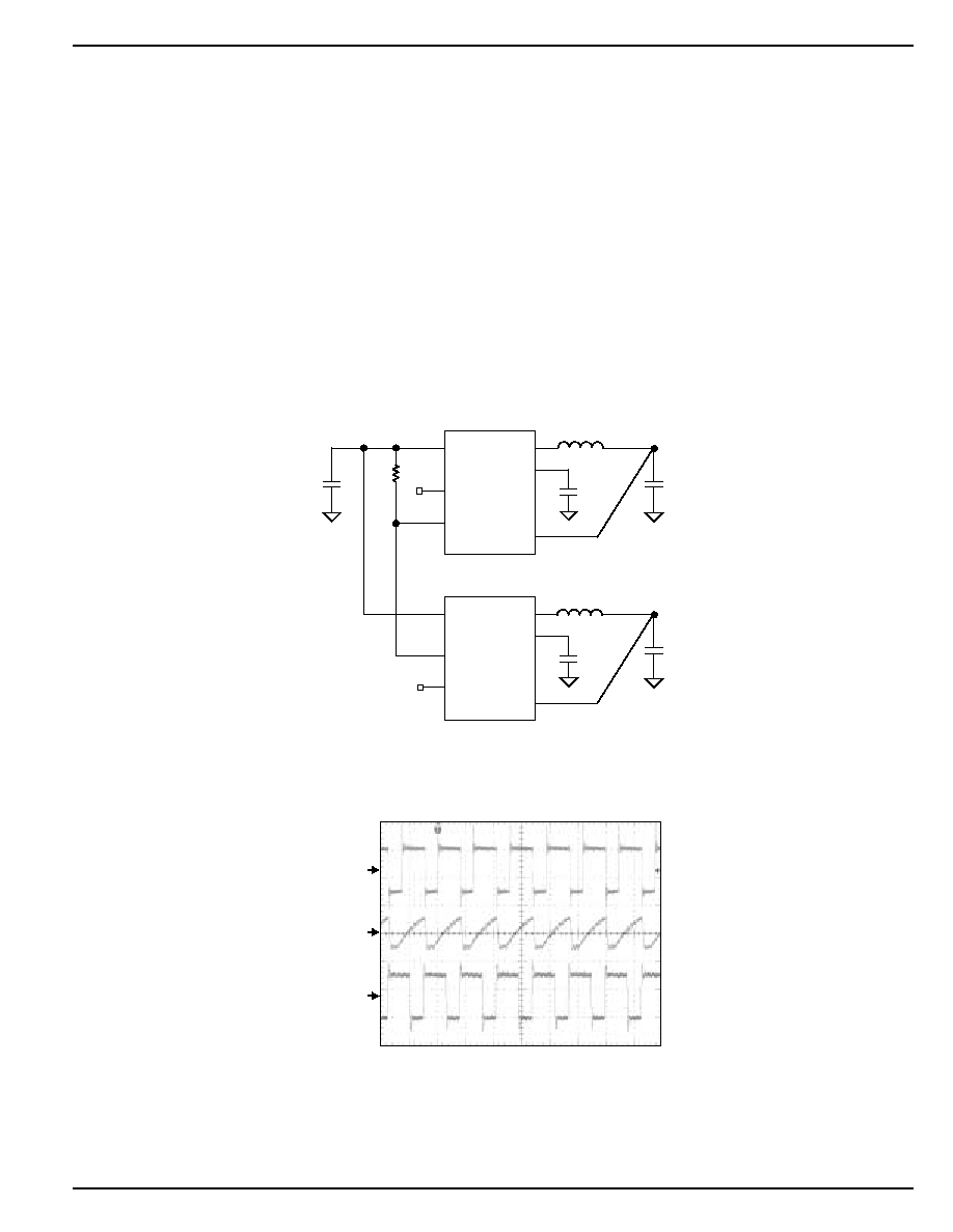
The Sync_Out function pin allows for the ability to be able to
sync up multiple MIC2202s in a "daisy-chain", connecting
Sync_Out to Sync_In of the other MIC2202. Synchronizing
multiple MIC2202s benefits much in the same way as syncing
up one MIC2202. All regulators will run at the same funda-
mental frequency, resulting in matched harmonic frequen-
cies, simplifying designing for sensitive communication equip-
ment.

MIC2202
Micrel
M9999-052104
10
May 2004
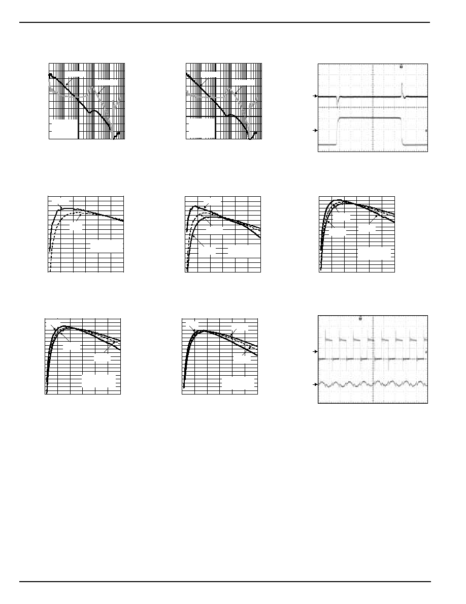
MIC2202BMM with 2.2
µ
H Inductor and 1
µ
F Output Capacitor
-30
-20
-10
0
10
20
30
40
50
60
70
-108
-72
-36
0
36
72
108
144
180
216
252
1x10
2
1x10
3
1x10
4
1x10
5
1x10
6
1x10
7
GAIN (dB)
PHASE (
∞
)
FREQUENCY (Hz)
Bode Plot
Phase
Gain
5V
IN
1.8V
OUT
L = 1
µ
H
C = 2.2
µ
F
-30
-20
-10
0
10
20
30
40
50
60
70
-108
-72
-36
0
36
72
108
144
180
216
252
1x10
2
1x10
3
1x10
4
1x10
5
1x10
6
1x10
7
GAIN (dB)
PHASE (
∞
)
FREQUENCY (Hz)
Bode Plot
Phase
Gain
3.6V
IN
1.8V
OUT
L = 1
µ
H
60
65
70
75
80
85
90
95
100
0
0.1
0.2
0.3
0.4
0.5
0.6
EFFICIENCY (%)
OUTPUT CURRENT (A)
Efficiency 3.3V
OUT
5V
IN
4.2V
IN
L = 2.2
µ
H
C
OUT
= 1
µ
F
60
65
70
75
80
85
90
95
100
0
0.1
0.2
0.3
0.4
0.5
0.6
EFFICIENCY (%)
OUTPUT CURRENT (A)
Efficiency 2.5V
OUT
3.6V
IN
3V
IN
L = 2.2
µ
H
C
OUT
= 1
µ
F
4.2V
IN
60
65
70
75
80
85
90
95
100
0
0.1
0.2
0.3
0.4
0.5
0.6
EFFICIENCY (%)
OUTPUT CURRENT (A)
Efficiency 1.8V
OUT
3.6V
IN
3V
IN
L = 2.2
µ
H
C
OUT
= 1
µ
F
4.2V
IN
60
65
70
75
80
85
90
95
100
0
0.1
0.2
0.3
0.4
0.5
0.6
EFFICIENCY (%)
OUTPUT CURRENT (A)
Efficiency 1.5V
OUT
3.6V
IN
3V
IN
L = 2.2
µ
H
C
OUT
= 1
µ
F
4.2V
IN
60
65
70
75
80
85
90
95
100
0
0.1
0.2
0.3
0.4
0.5
0.6
EFFICIENCY (%)
OUTPUT CURRENT (A)
Efficiency 1.2V
OUT
3.6V
IN
3V
IN
L = 2.2
µ
H
C
OUT
= 1
µ
F
4.2V
IN
Load Transient
TIME (40µs/div.)
I
OUT
200mA/div
L = 2.2µH
C = 1µF
V
IN
= 3.6V
V
OUT
= 1.8V
V
OUT
200mV/div
Vsw-Vripple
TIME (400ns/div.)
V
SW
2V/div
V
OUT
20mV/div
L = 2.2µH
C = 1µF
V
IN
= 3.6V
V
OUT
= 1.8V
I
OUT
= 600mA

May 2004
11
M9999-052104
MIC2202
Micrel
Bill of Materials
Item
Part Number
Manufacturer
Description
Qty.
C1, C3
06036D105MAT2
AVX
1uF Ceramic Capacitor X5R, 6.3V, Size 0603
2
GRM185R60J105KE21D
Murata
1uF Ceramic Capacitor X5R, 6.3V, Size 0603
C2
0201ZD103MAT2
AVX
10nF Cermaic Capacitor 6.3V, Size 0201
1
GRM033R10J103KA01D
Murata
10nF Cermaic Capacitor 6.3V, Size 0202
L1
LQH32CN2R2M53K
Murata
2.2uH Inductor 97m
(3.2mmx2.5mmx1.55mm)
1
CDRH2D14-2R2
Sumida
2.2uH Inductor 94m
(3.2mmx3.2mmx1.55mm)
R1
CRCW04021002F
Vishay-Dale
10k
1%, Size 0402
R2
CRCW04021781F
Vishay-Dale
1.78k
1%, Size 0402 For 3.3V
OUT
1
CRCW04022491F
Vishay-Dale
2.49k
1%, Size 0402 For 2.5V
OUT
CRCW04023831F
Vishay-Dale
3.83k
1%, Size 0402 For 1.8V
OUT
CRCW04024991F
Vishay-Dale
4.99k
1%, Size 0402 For 1.5V
OUT
CRCW04027151F
Vishay-Dale
7.15k
1%, Size 0402 For 1.2V
OUT
CRCW04021002F
Vishay-Dale
10k
1%, Size 0402
For 1V
OUT
N/A
Open
For 0.5V
OUT
U1
MIC2202BMM
Micrel, Inc.
2MHz High Efficiency Synchronous
1
Buck Regulator
1.
AVX: www.avx.com
2.
Murata: www.murata.com
3.
Sumida: www.sumida.com
4.
Vishay-Dale: www.vishay.com
5.
Micrel, Inc: www.micrel.com
V
IN
MIC2202BMM
EN
SYNC_OUT
VIN
VSW
BIAS
SYNC_IN
FB
GND
C2
0.01
µ
F
GND
2
5
4
3
7
GND
C3
1
µ
F
C1
1
µ
F
V
OUT
600mA
GND
1
6
10
9
8
L1
2.2
µ
H
R1
10k
R2
see BOM
for values
GND
Figure 6. MIC2202BMM Schematic
MIC2202BMM with 2.2
µ
H Inductor and 1
µ
F Output Capacitor

MIC2202
Micrel
M9999-052104
12
May 2004
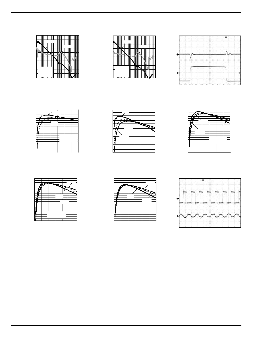
MIC2202BMM with 1
µ
H Inductor and 2.2
µ
F Output Capacitor
-30
-20
-10
0
10
20
30
40
50
60
70
-108
-72
-36
0
36
72
108
144
180
216
252
1x10
2
1x10
3
1x10
4
1x10
5
1x10
6
1x10
7
GAIN (dB)
PHASE (
∞
)
FREQUENCY (Hz)
Bode Plot
Phase
Gain
5V
IN
1.8V
OUT
L = 1
µ
H
-30
-20
-10
0
10
20
30
40
50
60
70
-108
-72
-36
0
36
72
108
144
180
216
252
1x10
2
1x10
3
1x10
4
1x10
5
1x10
6
1x10
7
GAIN (dB)
PHASE (
∞
)
FREQUENCY (Hz)
Bode Plot
Phase
Gain
3.6V
IN
1.8V
OUT
L = 1
µ
H
60
65
70
75
80
85
90
95
100
0
0.1
0.2
0.3
0.4
0.5
0.6
EFFICIENCY (%)
OUTPUT CURRENT (A)
Efficiency 3.3V
OUT
5V
IN
4.2V
IN
L = 1
µ
H
C
OUT
= 2.2
µ
F
60
65
70
75
80
85
90
95
100
0
0.1
0.2
0.3
0.4
0.5
0.6
EFFICIENCY (%)
OUTPUT CURRENT (A)
Efficiency 2.5V
OUT
4.2V
IN
3V
IN
L = 1
µ
H
C
OUT
= 2.2
µ
F
3.6V
IN
40
45
50
55
60
65
70
75
80
85
90
0
0.1
0.2
0.3
0.4
0.5
0.6
EFFICIENCY (%)
OUTPUT CURRENT (A)
Efficiency 1.8V
OUT
3.6V
IN
3V
IN
L = 1
µ
H
C
OUT
= 2.2
µ
F
4.2V
IN
40
45
50
55
60
65
70
75
80
85
90
0
0.1
0.2
0.3
0.4
0.5
0.6
EFFICIENCY (%)
OUTPUT CURRENT (A)
Efficiency 1.5V
OUT
3.6V
IN
3V
IN
L = 1
µ
H
C
OUT
= 2.2
µ
F
4.2V
IN
40
45
50
55
60
65
70
75
80
85
90
0
0.1
0.2
0.3
0.4
0.5
0.6
EFFICIENCY (%)
OUTPUT CURRENT (A)
Efficiency 1.2V
OUT
4.2V
IN
3V
IN
L = 1
µ
H
C
OUT
= 2.2
µ
F
3.6V
IN
Load Transient
TIME (40µs/div.)
I
OUT
200mA/div
L = 2.2µH
C = 1µF
V
IN
= 3.6V
V
OUT
= 1.8V
V
OUT
200mV/div
Vsw-Vripple
TIME (400ns/div.)
V
SW
2V/div
V
OUT
20mV/div
L = 2.2µH
C = 1µF
V
IN
= 3.6V
V
OUT
= 1.8V
I
OUT
= 600mA

May 2004
13
M9999-052104
MIC2202
Micrel
Bill of Materials
Item
Part Number
Manufacturer
Description
Qty.
C1
06036D105MAT2
AVX
1
µ
F Ceramic Capacitor X5R, 6.3V, Size 0603
1
GRM185R60J105KE21D
Murata
1
µ
F Ceramic Capacitor X5R, 6.3V, Size 0603
C2
0201ZD103MAT2
AVX
10nF Cermaic Capacitor 6.3V, Size 0201
1
GRM033R10J103KA01D
Murata
10nF Cermaic Capacitor 6.3V, Size 0202
C3
06036D225MAT2
AVX
2.2
µ
F Ceramic Capacitor X5R, 6.3V, Size 0603
1
GRM033R10J103KA01D
Murata
2.2
µ
F Ceramic Capacitor X5R, 6.3V, Size 0603
L1
LQH32CN1R0M53K
Murata
1
µ
H Inductor 60m
(3.2mmx2.5mmx1.55mm)
1
CDRH2D14-2R2
Sumida
1.5
µ
H Inductor 63m
(3.2mmx3.2mmx1.55mm)
R1
CRCW04021002F
Vishay-Dale
10k
1%, Size 0402
1
R2
CRCW04021781F
Vishay-Dale
1.78k
1%, Size 0402 For 3.3V
OUT
1
CRCW04022491F
Vishay-Dale
2.49k
1%, Size 0402 For 2.5V
OUT
CRCW04023831F
Vishay-Dale
3.83k
1%, Size 0402 For 1.8V
OUT
CRCW04024991F
Vishay-Dale
4.99k
1%, Size 0402 For 1.5V
OUT
CRCW04027151F
Vishay-Dale
7.15k
1%, Size 0402 For 1.2V
OUT
CRCW04021002F
Vishay-Dale
10k
1%, Size 0402
For 1V
OUT
N/A
Open
For 0.5V
OUT
U1
MIC2202BMM
Micrel, Inc.
2MHz High Efficiency Synchronous
1
Buck Regulator
1.
AVX: www.avx.com
2.
Murata: www.murata.com
3.
Sumida: www.sumida.com
4.
Vishay-Dale: www.vishay.com
5.
Micrel, Inc: www.micrel.com
V
IN
MIC2202BMM
EN
SYNC_OUT
VIN
VSW
BIAS
SYNC_IN
FB
GND
C2
0.01
µ
F
GND
2
5
4
3
7
GND
C3
2.2
µ
F
C1
1
µ
F
V
OUT
600mA
GND
1
6
10
9
8
L1
1
µ
H
R1
10k
R2
see BOM
for values
GND
Figure 7. MIC2202BMM Schematic
MIC2202BMM with 1
µ
H Inductor and 2.2
µ
F Output Capacitor

MIC2202
Micrel
M9999-052104
14
May 2004
MIC2202BMM with 4.7
µ
H Inductor and 1
µ
F Output Capacitor
-30
-20
-10
0
10
20
30
40
50
60
70
-108
-72
-36
0
36
72
108
144
180
216
252
1x10
2
1x10
3
1x10
4
1x10
5
1x10
6
1x10
7
GAIN (dB)
PHASE (
∞
)
FREQUENCY (Hz)
Bode Plot
Phase
Gain
5V
IN
1.8V
OUT
L = 4.7
µ
H
-30
-20
-10
0
10
20
30
40
50
60
70
-108
-72
-36
0
36
72
108
144
180
216
252
1x10
2
1x10
3
1x10
4
1x10
5
1x10
6
1x10
7
GAIN (dB)
PHASE (
∞
)
FREQUENCY (Hz)
Bode Plot
Phase
Gain
3.6V
IN
1.8V
OUT
L = 4.7
µ
H
70
75
80
85
90
95
100
0
0.1
0.2
0.3
0.4
0.5
0.6
EFFICIENCY (%)
OUTPUT CURRENT (A)
Efficiency 3.3V
OUT
5V
IN
L = 4.7
µ
H
C
OUT
= 1
µ
F
4.2V
IN
60
65
70
75
80
85
90
95
100
0
0.1
0.2
0.3
0.4
0.5
0.6
EFFICIENCY (%)
OUTPUT CURRENT (A)
Efficiency 2.5V
OUT
4.2V
IN
L = 4.7
µ
H
C
OUT
= 1
µ
F
3.6V
IN
3V
IN
60
65
70
75
80
85
90
95
0
0.1
0.2
0.3
0.4
0.5
0.6
EFFICIENCY (%)
OUTPUT CURRENT (A)
Efficiency 1.8V
OUT
3V
IN
L = 4.7
µ
H
C
OUT
= 1
µ
F
4.2V
IN
3.6V
IN
60
65
70
75
80
85
90
95
0
0.1
0.2
0.3
0.4
0.5
0.6
EFFICIENCY (%)
OUTPUT CURRENT (A)
Efficiency 1.5V
OUT
3.6V
IN
3V
IN
L = 4.7
µ
H
C
OUT
= 1
µ
F
4.2V
IN
60
65
70
75
80
85
90
95
0
0.1
0.2
0.3
0.4
0.5
0.6
EFFICIENCY (%)
OUTPUT CURRENT (A)
Efficiency 1.2V
OUT
4.2V
IN
3V
IN
L = 4.7
µ
H
C
OUT
= 1
µ
F
3.6V
IN
Load Transient
TIME (40µs/div.)
I
OUT
200mA/div
L = 4.7µH
C = 1µF
V
IN
= 3.6V
V
OUT
= 1.8V
V
OUT
200mV/div
Vsw-Vripple
TIME (400ns/div.)
V
SW
2V/div
V
OUT
20mV/div
L = 4.7µH
C = 1µF
V
IN
= 3.6V
V
OUT
= 1.8V
I
OUT
= 600mA

May 2004
15
M9999-052104
MIC2202
Micrel
Bill of Materials
Item
Part Number
Manufacturer
Description
Qty.
C1, C3
06036D105MAT2
AVX
1uF Ceramic Capacitor X5R, 6.3V, Size 0603
2
GRM185R60J105KE21D
Murata
1uF Ceramic Capacitor X5R, 6.3V, Size 0603
C2
0201ZD103MAT2
AVX
10nF Cermaic Capacitor 6.3V, Size 0201
1
GRM033R10J103KA01D
Murata
10nF Cermaic Capacitor 6.3V, Size 0202
L1
LQH32CN4R7M53K
Murata
4.7uH Inductor 150m
(3.2mmx2.5mmx1.55mm)
1
CDRH2D14-4R7
Sumida
4.7uH Inductor 169m
(3.2mmx3.2mmx1.55mm)
R1
CRCW04021002F
Vishay-Dale
10k
1%, Size 0402
1
R2
CRCW04021781F
Vishay-Dale
1.78k
1%, Size 0402 For 3.3V
OUT
1
CRCW04022491F
Vishay-Dale
2.49k
1%, Size 0402 For 2.5V
OUT
CRCW04023831F
Vishay-Dale
3.83k
1%, Size 0402 For 1.8V
OUT
CRCW04024991F
Vishay-Dale
4.99k
1%, Size 0402 For 1.5V
OUT
CRCW04027151F
Vishay-Dale
7.15k
1%, Size 0402 For 1.2V
OUT
CRCW04021002F
Vishay-Dale
10k
1%, Size 0402
For 1V
OUT
N/A
Open
For 0.5V
OUT
U1
MIC2202BMM
Micrel, Inc.
2MHz High Efficiency Synchronous
1
Buck Regulator
1.
AVX: www.avx.com
2.
Murata: www.murata.com
3.
Sumida: www.sumida.com
4.
Vishay-Dale: www.vishay.com
5.
Micrel, Inc: www.micrel.com
V
IN
MIC2202BMM
EN
SYNC_OUT
VIN
VSW
BIAS
SYNC_IN
FB
GND
C2
0.01
µ
F
GND
2
5
4
3
7
GND
C3
1
µ
F
C1
1
µ
F
V
OUT
600mA
GND
1
6
10
9
8
L1
4.7
µ
H
R1
10k
R2
see BOM
for values
GND
Figure 8. MIC2202BMM Schematic
MIC2202BMM with 4.7
µ
H Inductor and 1
µ
F Output Capacitor

MIC2202
Micrel
M9999-052104
16
May 2004
MIC2202BMM with 1
µ
H Inductor and 4.7
µ
F Output Capacitor
-30
-20
-10
0
10
20
30
40
50
60
70
-108
-72
-36
0
36
72
108
144
180
216
252
1x10
2
1x10
3
1x10
4
1x10
5
1x10
6
1x10
7
GAIN (dB)
PHASE (
∞
)
FREQUENCY (Hz)
Bode Plot
Phase
Gain
5V
IN
1.8V
OUT
L = 1
µ
H
-30
-20
-10
0
10
20
30
40
50
60
70
-108
-72
-36
0
36
72
108
144
180
216
252
1x10
2
1x10
3
1x10
4
1x10
5
1x10
6
1x10
7
GAIN (dB)
PHASE (
∞
)
FREQUENCY (Hz)
Bode Plot
Phase
Gain
3.6V
IN
1.8V
OUT
L = 1
µ
H
50
55
60
65
70
75
80
85
90
95
100
0
0.1
0.2
0.3
0.4
0.5
0.6
EFFICIENCY (%)
OUTPUT CURRENT (A)
Efficiency 3.3V
OUT
5V
IN
L = 1
µ
H
C
OUT
= 4.7
µ
F
4.2V
IN
60
65
70
75
80
85
90
95
100
0
0.1
0.2
0.3
0.4
0.5
0.6
EFFICIENCY (%)
OUTPUT CURRENT (A)
Efficiency 2.5V
OUT
4.2V
IN
L = 1
µ
H
C
OUT
= 4.7
µ
F
3.6V
IN
3V
IN
40
45
50
55
60
65
70
75
80
85
90
0
0.1
0.2
0.3
0.4
0.5
0.6
EFFICIENCY (%)
OUTPUT CURRENT (A)
Efficiency 1.8V
OUT
3V
IN
L = 1
µ
H
C
OUT
= 4.7
µ
F
4.2V
IN
3.6V
IN
40
45
50
55
60
65
70
75
80
85
90
0
0.1
0.2
0.3
0.4
0.5
0.6
EFFICIENCY (%)
OUTPUT CURRENT (A)
Efficiency 1.5V
OUT
3.6V
IN
3V
IN
L = 1
µ
H
C
OUT
= 4.7
µ
F
4.2V
IN
40
45
50
55
60
65
70
75
80
85
90
0
0.1
0.2
0.3
0.4
0.5
0.6
EFFICIENCY (%)
OUTPUT CURRENT (A)
Efficiency 1.2V
OUT
4.2V
IN
3V
IN
L = 1
µ
H
C
OUT
= 4.7
µ
F
3.6V
IN
Load Transient
TIME (40µs/div.)
I
OUT
200mA/div
L = 1µH
C = 4.7µF
V
IN
= 3.6V
V
OUT
= 1.8V
V
OUT
200mV/div
Vsw-Vripple
TIME (400ns/div.)
V
SW
2V/div
V
OUT
20mV/div
L = 1µH
C = 4.7µF
V
IN
= 3.6V
V
OUT
= 1.8V
I
OUT
= 600mA

May 2004
17
M9999-052104
MIC2202
Micrel
Bill of Materials
Item
Part Number
Manufacturer
Description
Qty.
C1
06036D105MAT2
AVX
1
µ
F Ceramic Capacitor X5R, 6.3V, Size 0603
1
GRM185R60J105KE21D
Murata
1
µ
F Ceramic Capacitor X5R, 6.3V, Size 0603
C2
0201ZD103MAT2
AVX
10nF Cermaic Capacitor 6.3V, Size 0201
1
GRM033R10J103KA01D
Murata
10nF Cermaic Capacitor 6.3V, Size 0202
C3
06036D475MAT2
AVX
4.7
µ
F Cermaic Capacitor 4V, Size 0201
1
GRM033R10J103KA01D
Murata
4.7
µ
F Cermaic Capacitor 6.3V, Size 0202
L1
LQH32CN1R0M53K
Murata
1
µ
H Inductor 60m
(3.2mmx2.5mmx1.55mm)
1
CDRH2D14-1R5
Sumida
1.5
µ
H Inductor 63m
(3.2mmx3.2mmx1.55mm)
R1
CRCW04021002F
Vishay-Dale
10k
1%, Size 0402
1
R2
CRCW04021781F
Vishay-Dale
1.78k
1%, Size 0402 For 3.3V
OUT
1
CRCW04022491F
Vishay-Dale
2.49k
1%, Size 0402 For 2.5V
OUT
CRCW04023831F
Vishay-Dale
3.83k
1%, Size 0402 For 1.8V
OUT
CRCW04024991F
Vishay-Dale
4.99k
1%, Size 0402 For 1.5V
OUT
CRCW04027151F
Vishay-Dale
7.15k
1%, Size 0402 For 1.2V
OUT
CRCW04021002F
Vishay-Dale
10k
1%, Size 0402
For 1V
OUT
N/A
Open
For 0.5V
OUT
U1
MIC2202BMM
Micrel, Inc.
2MHz High Efficiency Synchronous
1
Buck Regulator
1.
AVX: www.avx.com
2.
Murata: www.murata.com
3.
Sumida: www.sumida.com
4.
Vishay-Dale: www.vishay.com
5.
Micrel, Inc: www.micrel.com
V
IN
MIC2202BMM
EN
SYNC_OUT
VIN
VSW
BIAS
SYNC_IN
FB
GND
C2
0.01
µ
F
GND
2
5
4
3
7
GND
C3
4.7
µ
F
C1
1
µ
F
V
OUT
600mA
GND
1
6
10
9
8
L1
1
µ
H
R1
10k
R2
see BOM
for values
GND
Figure 9. MIC2202BMM Schematic
MIC2202BMM with 1
µ
H Inductor and 4.7
µ
F Output Capacitor

MIC2202
Micrel
M9999-052104
18
May 2004
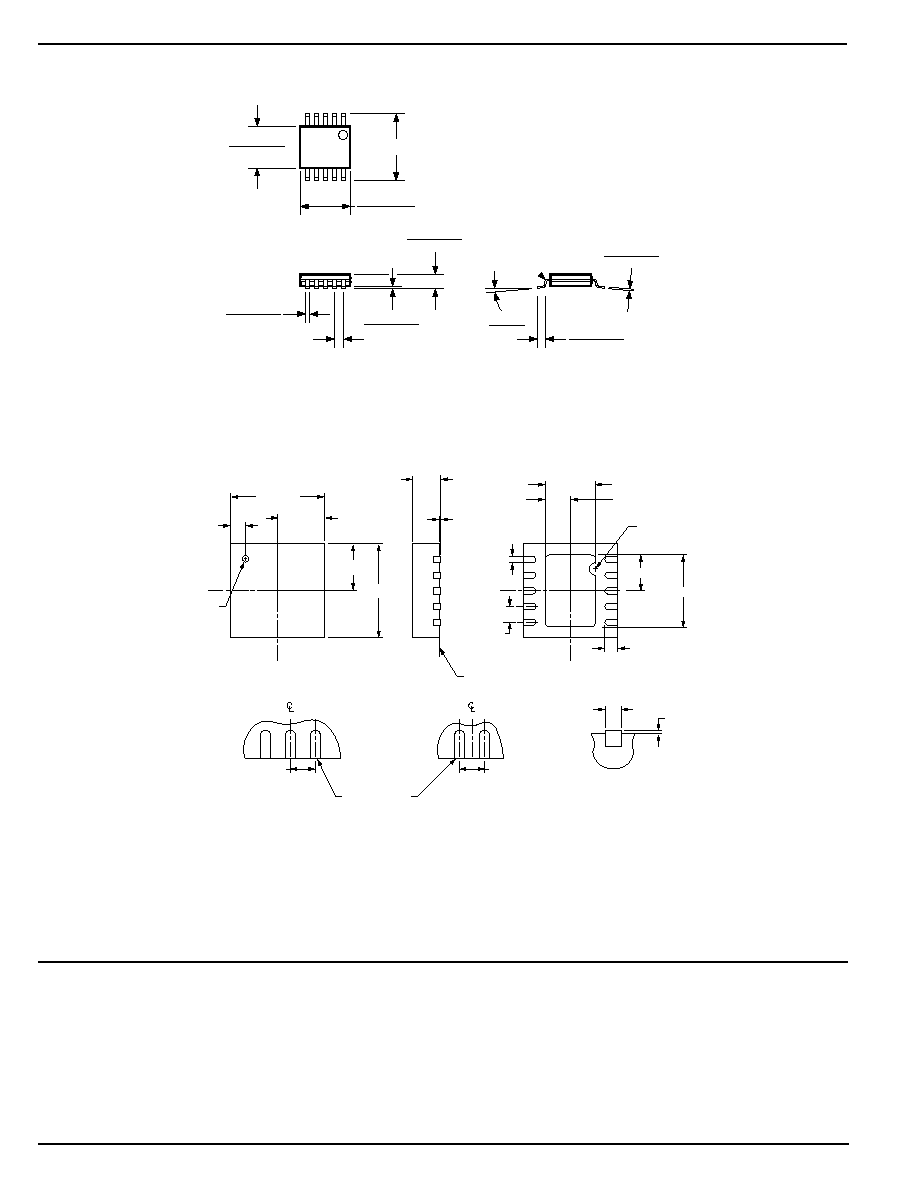
Package Information
0.15 (0.006)
0.05 (0.002)
0.50 BSC (0.020)
6
∞
MAX
0
∞
MIN
3.15 (0.122)
2.85 (0.114)
3.10 (0.122)
2.90 (0.114)
0.30 (0.012)
0.15 (0.006)
0.26 (0.010)
0.10 (0.004)
1.10 (0.043)
0.94 (0.037)
DIMENSIONS:
MM (INCH)
0.70 (0.028)
0.40 (0.016)
4.90 BSC (0.193)
10-Pin MSOP (MM)
0.20 dia
0.48 typ.
3.00 BSC.
1.50 BSC.
PIN 1 ID
0.85
3.00 BSC.
TOP
BOTTOM
ODD TERMINAL SIDE
EVEN TERMINAL SIDE
TERMINAL TIP
TERMINAL TIP
1.50 BSC.
1
2
3
1
2
3
≠0.05
+0.15
0.01
0.50 BSC.
0.50 BSC.
0.50 BSC.
≠0.01
+0.04
0.23
≠0.05
+0.07
0.23
≠0.05
+0.07
0.01
≠0.01
+0.04
0.40
≠0.05
+0.15
1.60
≠0.15
+0.15
0.80
≠0.15
+0.15
2.30
≠0.15
+0.15
1.15
≠0.15
+0.15
SEATING PLANE
DIMENSIONS: mm
10-Pin MLFTM (ML)
MICREL, INC.
1849 FORTUNE DRIVE
SAN JOSE, CA 95131
USA
TEL
+ 1 (408) 944-0800
FAX
+ 1 (408) 474-1000
WEB
http://www.micrel.com
The information furnished by Micrel in this data sheet is believed to be accurate and reliable. However, no responsibility is assumed by Micrel for its use.
Micrel reserves the right to change circuitry and specifications at any time without notification to the customer.
Micrel Products are not designed or authorized for use as components in life support appliances, devices or systems where malfunction of a product can
reasonably be expected to result in personal injury. Life support devices or systems are devices or systems that (a) are intended for surgical implant into
the body or (b) support or sustain life, and whose failure to perform can be reasonably expected to result in a significant injury to the user. A Purchaser's
use or sale of Micrel Products for use in life support appliances, devices or systems is at Purchaser's own risk and Purchaser agrees to fully indemnify
Micrel for any damages resulting from such use or sale.
© 2004 Micrel, Incorporated.


