 | –≠–ª–µ–∫—Ç—Ä–æ–Ω–Ω—ã–π –∫–æ–º–ø–æ–Ω–µ–Ω—Ç: MIC2208 | –°–∫–∞—á–∞—Ç—å:  PDF PDF  ZIP ZIP |

MIC2208
3mmx3mm 1MHz 3A PWM Buck
Regulator
General Description
The Micrel MIC2208 is a high efficiency PWM buck
(step-down) regulator that provides up to 3A of
output current. The MIC2208 operates at 1MHz and
has external compensation that allows a closed loop
bandwidth of over 100KHz.
The low on-resistance internal p-channel MOSFET
of the MIC2208 allows efficiencies over 94%,
reduces external component count and eliminates
the need for an expensive current sense resistor.
The MIC2208 operates from 2.7V to 5.5V input and
the output can be adjusted down to 1V. The devices
can operate with a maximum duty cycle of 100% for
use in low-dropout conditions.
The MIC2208 is available in the exposed pad 3mm x
3mm MLF-12L package with a junction operating
range from ≠40∞C to +125∞C.
Features
∑ 2.7 to 5.5V supply voltage
∑ 1MHz
PWM
mode
∑ Output current to 3A
∑ >90%
efficiency
∑ Adjustable output voltage option down to 1V
∑ Ultra-fast transient response
∑ External
Compensation
∑ Stable with a wide range of output
capacitance
∑ Fully integrated 5A MOSFET switch
∑ Micropower
shutdown
∑ Thermal shutdown and current limit
protection
∑ Pb-free 3mm x 3mm MLF-10L package
∑ ≠40∞C to +125∞C junction temperature range
∑ Internal
soft-start
Applications
∑ 5V or 3.3V Point of Load Conversion
∑ Telecom/Networking Equipment
∑ Set Top Boxes
∑ Storage
Equipment
∑ Video
Cards
Typical Application
MIC2208
3A 1MHz Buck Regulator
MLF and
Micro
LeadFrame are trademarks of Amkor Technology
Micrel, Inc ∑ 2180 Fortune Drive ∑ San Jose, Ca 95131 ∑ USA ∑ tel +1 (408) 944-0800 ∑ fax +1 (408) 474-1000 ∑ http://www.micrel.com
September 2005
M9999-092905
www.micrel.com

Micrel, Inc.
MIC2208
Ordering Information
Part Number
Output
Voltage
(1)
Junction Temp. Range
Package
Lead Finish
MIC2208YML
Adj.
≠40∞ to +125∞C
3mmx3mm MLF-10L
Pb-free
.
Pin Configuration
BIAS
EN
SW
VIN
PGND
SGND
SW
VIN
PGND
PGOOD
5
1
2
3
4
8
FB
COMP
6
7
12
11
10
9
EP
3mm x 3mm MLF-12 (ML)
Pin Description
Pin Number
Pin Name
Pin Function
1,12
SW
Switch (Output): Internal power P-Channel MOSFET output switch
2,11 VIN
Supply Voltage (Input): Supply voltage for the source of the internal P-channel
MOSFET and driver.
Requires bypass capacitor to GND.
3,10
PGND
Power Ground. Provides the ground return path for the high-side drive current.
4
SGND
Signal Ground. Provides return path for control circuitry and internal reference.
5
BIAS
Internal circuit bias supply. Must be bypassed with a 0.1uF ceramic capacitor to
SGND.
6 FB
Feedback. Input to the error amplifier, connect to the external resistor divider
network to set the output voltage.
7 COMP
Compensation. This is the internal error amplifier output. Connect external
compensation components for type II or type III compensation.
8 EN
Enable (Input). Logic level low will shutdown the device, reducing the current
draw to less than 5uA.
9 PGOOD
Power Good. Open drain output that is pulled to ground when the output voltage
is within +/- 7.5% of the set regulation voltage
EP
GND
Connect to ground.
September 2005
2
M9999-092905
www.micrel.com

Micrel, Inc.
MIC2208
Absolute Maximum Ratings
(1)
Supply Voltage (V
IN
) ...............................-0.3V to +6V
Output Switch Voltage (V
SW
) .....................-1V to +6V
Output Switch Current (I
SW
) ................................. 10A
Logic Input Voltage (V
EN
)......................... -0.3V to V
IN
Storage Temperature (T
s
)................ -60∞C to +150∞C
ESD Rating
(3)
............................................2KV (HBM)
Operating Ratings
(2)
Supply Voltage (V
IN
)............................+2.7V to +5.5V
Logic Input Voltage (V
EN
,V
LOWQ
) .................. 0V to V
IN
Junction Temperature (T
J
) .............. ≠40∞C to +125∞C
Junction Thermal Resistance
3mmx3mm MLF-12L (
JA
) ....................... 60∞C/W
Electrical Characteristics
(4)
V
IN
= V
EN
= 3.6V; L = 1
µH; C
OUT
= 4.7
µF; T
A
= 25∞C, unless noted.
Bold
values indicate ≠40∞C< T
J
< +125∞C
Parameter Condition
Min
Typ
Max
Units
Supply Voltage Range
2.7
5.5
V
Under-Voltage Lockout
Threshold
(turn-on)
2.45
2.55
2.65
V
UVLO Hysteresis
100
mV
Quiescent Current
V
FB
= 0.9 * V
NOM
(not switching)
720
950
µA
Shutdown Current
V
EN
= 0V
0.1
5
µA
[Adjustable] Feedback
Voltage
± 1%
± 2% (over temperature)
0.99
0.98
1
1.01
1.02
V
FB pin input current
1
100
nA
Current Limit in PWM Mode V
FB
= 0.9 * V
NOM
8
10
A
Output Voltage Line
Regulation
V
OUT
> 2.2V; V
IN
= V
OUT
+500mV to 5.5V; I
LOAD
= 20mA
V
OUT
< 2.2V; V
IN
= 2.7V to 5.5V; I
LOAD
= 20mA
0.13 %
Output Voltage Load
Regulation
20mA < I
LOAD
< 3A
0.2
1
%
PWM Switch ON-
Resistance
I
SW
= 50mA V
FB
= 0.7V
FB_NOM
(High Side Switch)
95
200
300
m
Oscillator Frequency
0.9
1
1.1
MHz
Enable Threshold
0.5
0.85
1.3
V
Enable Input Current
0.1
2
µA
Soft Start Time
V
OUT
=10% to V
OUT
=90%
450 µs
Over-Temperature
Shutdown
160
∞C
over-Temperature
Hysteresis
20
∞C
Power Good Range
±7
±10
%
Power Good Resistance
I
PGOOD
145
200
Notes:
1. Exceeding the absolute maximum rating may damage the device.
2. The device is not guaranteed to function outside its operating rating.
3. Devices are ESD sensitive. Handling precautions recommended. Human body model: 1.5k
in series with 100pF.
4. Specification for packaged product only.
September 2005
3
M9999-092905
www.micrel.com

Micrel, Inc.
MIC2208
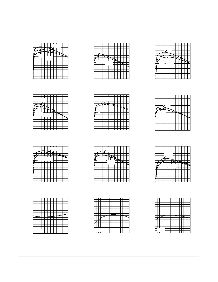
Typical Characteristics
80
82
84
86
88
90
92
94
96
0
0.5
1
1.5
2
2.5
3
EF
FICIENCY (%)
OUTPUT CURRENT (A)
MIC2208
3.3V
OUT
Efficiency
4.5V
IN
5V
IN
5.5V
IN
80
82
84
86
88
90
92
94
96
98
100
0
0.5
1
1.5
2
2.5
3
EF
FICIENCY (%)
OUTPUT CURRENT (A)
MIC2207
2.5V
OUT
Efficiency
3.3V
IN
3.6V
IN
80
82
84
86
88
90
92
94
0
0.5
1
1.5
2
2.5
3
EF
FICIENCY (%)
OUTPUT CURRENT (A)
MIC2207
2.5V
OUT
Efficiency
5.5V
IN
5V
IN
4.5V
IN
75
77
79
81
83
85
87
89
91
93
95
0
0.5
1
1.5
2
2.5
3
EFFICIE
NCY (%)
OUTPUT CURRENT (A)
MIC2208
1.8V
OUT
Efficiency
3.6V
IN
3V
IN
3.3V
IN
70
72
74
76
78
80
82
84
86
88
90
0
0.5
1
1.5
2
2.5
3
EFFICIE
NCY (%)
OUTPUT CURRENT (A)
MIC2208
1.8V
OUT
Efficiency
4.5V
IN
5V
IN
70
75
80
85
90
95
0
0.5
1
1.5
2
2.5
3
EF
FICIENCY (%)
OUTPUT CURRENT (A)
MIC2208
1.5V
OUT
Efficiency
3.3V
IN
3V
IN
3.6V
IN
65
67
69
71
73
75
77
79
81
83
85
0
0.5
1
1.5
2
2.5
3
E
FFICIENC
Y
(
%
)
OUTPUT CURRENT (A)
MIC2208
1.5V
OUT
Efficiency
5.5V
IN
5V
IN
4.5V
IN
65
67
69
71
73
75
77
79
81
83
85
0
0.5
1
1.5
2
2.5
3
E
FFICIENC
Y
(
%
)
OUTPUT CURRENT (A)
MIC2208
1.2V
OUT
Efficiency
3.6V
IN
3V
IN
3.3V
IN
65
67
69
71
73
75
77
79
81
83
85
0
0.5
1
1.5
2
2.5
3
E
FFICIENC
Y
(
%
)
OUTPUT CURRENT (A)
MIC2208
1.2V
OUT
Efficiency
5.5V
IN
5V
IN
4.5V
IN
0.990
0.992
0.994
0.996
0.998
1.000
1.002
1.004
1.006
1.008
1.010
0
0.5
1
1.5
2
2.5
3
OUTPUT
VO
L
T
AGE (V)
OUTPUT CURRENT (A)
Load Regulation
3.3V
IN
0.9900
0.9920
0.9940
0.9960
0.9980
1.0000
1.0020
1.0040
1.0060
1.0080
1.0100
-4
0
-2
0
0
20
40
60
80
10
0
12
0
FE
EDB
AC
K VO
L
T
A
G
E (V
)
TEMPERATURE (∞C)
Feedback Voltage
vs. Temperature
3.3V
IN
0.80
0.85
0.90
0.95
1.00
1.05
1.10
1.15
1.20
-4
0
-2
0
0
20
40
60
80
10
0
12
0
FE
EDB
AC
K VO
L
T
A
G
E (V
)
TEMPERATURE (∞C)
Feedback Voltage
vs. Temperature
3.3V
IN
September 2005
4
M9999-092905
www.micrel.com

Micrel, Inc.
MIC2208
0
0.2
0.4
0.6
0.8
1.0
1.2
0
1
2
3
4
5
FEED
BACK VOLT
AG
E (V)
SUPPLY VOLTAGE (V)
Feedback Voltage
vs. Supply Voltage
0
100
200
300
400
500
600
700
0
1
2
3
4
5
Q
U
IES
C
ENT CUR
RENT (µA)
SUPPLY VOLTAGE (V)
Quiescent Current
vs. Supply Voltage
70
75
80
85
90
95
100
105
110
115
120
2.7
3.2
3.7
4.2
4.7
5.2
P-CHAN
N
EL RDS
O
N
(m
Ohm
s
)
SUPPLY VOLTAGE (V)
RDSON
vs. Supply Voltage
0
20
40
60
80
100
120
140
160
-4
0
-2
0
0
20
40
60
80
10
0
12
0
P
-
CH
AN
NE
L RD
SO
N (mOh
ms)
TEMPERATURE (∞C)
RDSON
vs. Temperature
3.3V
IN
0
0.2
0.4
0.6
0.8
1
1.2
2.7
3.2
3.7
4.2
4.7
ENABL
E THRE
SHO
L
D (V)
SUPPLY VOLTAGE (V)
Enable Threshold
vs. Supply Voltage
0
0.2
0.4
0.6
0.8
1
1.2
-4
0
-2
0
0
20
40
60
80
10
0
12
0
EN
ABL
E TH
RE
SH
O
L
D
(
V
)
TEMPERATURE (∞C)
Enable Threshold
vs. Temperature
0
0.5
1
1.5
2
2.5
3
3.5
60
70
80
90 100 110 120
M
AX. OUTPUT
CURRENT
(
A
)
AMBIENT TEMPERATURE (∞C)
Max. Continuous Current
vs. Ambient Temp 3.3V
OUT
*
*Using recommended
layout (1oz copper)
and B.O.M.
5V
IN
0
0.5
1
1.5
2
2.5
3
3.5
60
70
80
90 100 110 120
M
AX. OUTPUT
CURRENT
(
A
)
AMBIENT TEMPERATURE (∞C)
Max. Continuous Current
vs. Ambient Temp 2.5V
OUT
*
*Using
recommended
layout (1oz copper)
and B.O.M.
3.3V
IN
5V
IN
0
0.5
1
1.5
2
2.5
3
3.5
60
70
80
90 100 110 120
M
AX. OUTPUT
CURRENT
(
A
)
AMBIENT TEMPERATURE (∞C)
Max. Continuous Current
vs. Ambient Temp 1.8V
OUT
*
*Using
recommended
layout (1oz copper)
and B.O.M.
3.3V
IN
5V
IN
0
0.5
1
1.5
2
2.5
3
3.5
60
70
80
90 100 110 120
M
AX. OUTPUT
CURRENT
(
A
)
AMBIENT TEMPERATURE (∞C)
Max. Continuous Current
vs. Ambient Temp 1.0V
OUT
*
*Using
recommended
layout (1oz copper)
and B.O.M.
3.3V
IN
5V
IN
September 2005
5
M9999-092905
www.micrel.com

Micrel, Inc.
MIC2208
Functional Diagram
VIN
VIN
BIAS
EN
SW
SW
FB
PGOOD
PGND
Enable and
Control Logic
PWM
Control
P-Channel
Current Limit
SGND
1.0V
1.0V
Soft
Start
Bias,
UVLO,
Thermal
Shutdown
HSD
EA
COMP
MIC2208 Block Diagram
September 2005
6
M9999-092905
www.micrel.com

Micrel, Inc.
MIC2208
Functional Characteristics
Continuous Operation
TIME (200ns/div.)
SWI
T
CH VO
LT
A
G
E
(2V/di
v
.
)
INDUC
T
O
R CURREN
T
(500mA/di
v
.
)
V
IN
= 3.3V
V
OUT
= 1V@1A
0A
Discontinuous Operation
TIME (200ns/div.)
SWI
T
CH VO
LT
A
G
E
(2V/di
v
.
)
INDUC
T
O
R CURREN
T
(200mA/di
v.
)
V
IN
= 3.3V
V
OUT
= 1V@0.15A
0A
Transient Response
TIME (100µs/div.)
OUTPU
T
VO
L
T
AG
E
(100mV/di
v.
)
OUTPU
T
CURREN
T
(2A/di
v
.
)
V
IN
= 3.3V. 1V, 3A to 200mA
0A
Enable Response
TIME (100µs/div.)
INPU
T
CURREN
T
(1A/di
v
.
)
INDUC
T
O
R CURREN
T
(2A/di
v
.
)
ENABLE
(5V/di
v
.
)
OUTPU
T
VO
L
T
AG
E
(1V/di
v
.
)
V
IN
= 3.3V
V
OUT
= 1V@3A
Power Good
TIME (100µs/div.)
POWER GOOD
(5V/di
v
.
)
ENABLE
(5V/di
v
.
)
OUTPU
T
VO
L
T
AG
E
(1V/di
v
.
)
V
IN
= 3.3V
Power Good
TIME (40µs/div.)
POWER GOOD
(5V/di
v
.
)
ENABLE
(5V/di
v
.
)
OUTPU
T
VO
L
T
AG
E
(1V/di
v
.
)
V
IN
= 3.3V
September 2005
7
M9999-092905
www.micrel.com

Micrel, Inc.
MIC2208
Pin Description
VIN
Two pins for VIN provide power to the source of the
internal P-channel MOSFET along with the current
limiting sensing. The VIN operating voltage range is
from 2.7V to 5.5V. Due to the high switching speeds,
a 10
µF capacitor is recommended close to VIN and
the power ground (PGND) for each pin for
bypassing. Please refer to layout recommendations.
BIAS
The bias (BIAS) provides power to the internal
reference and control sections of the MIC2208. A 10
Ohm resistor from VIN to BIAS and a 0.1uF from
BIAS to SGND is required for clean operation.
EN
The enable pin provides a logic level control of the
output. In the off state, supply current of the device
is greatly reduced (typically <1
µA). Do not drive the
enable pin above the supply voltage.
FB
The feedback pin (FB) provides the control path to
control the output. For adjustable versions, a resistor
divider connecting the feedback to the output is used
to adjust the desired output voltage. The output
voltage is calculated as follows:
+
◊
=
1
R2
R1
V
V
REF
OUT
where V
REF
is equal to 1.0V.
COMP
The COMP pin is the output of the internal error
amplifier. This pin is used to compensate the
MIC2208 for stability over a varying range of
external components. Refer to the compensation
section of the datasheet for determining nessasary
component values.
SW
The switch (SW) pin connects directly to the inductor
and provides the switching current nessasary to
operate in PWM mode. Due to the high speed
switching on this pin, the switch node should be
routed away from sensitive nodes. This pin also
connects to the cathode of the free-wheeling diode.
PGOOD
Power good is an open drain pull down that
indicates when the output voltage has reached
regulation. For a power good low, the output voltage
is within +/- 10% of the set regulation voltage. For
output voltages greater or less than 10%, the
PGOOD pin is high. This should be connected to the
input supply through a pull up resistor. A delay can
be added by placing a capacitor from PGOOD to
ground.
PGND
Power ground (PGND) is the ground path for the
MOSFET drive current. The current loop for the
power ground should be as small as possible and
separate from the Analog ground (AGND) loop.
Refer to the layout considerations fro more details.
SGND
Signal ground (SGND) is the ground path for the
biasing and control circuitry. The current loop for the
signal ground should be separate from the power
ground (PGND) loop. Refer to the layout
considerations for more details.
September 2005
8
M9999-092905
www.micrel.com

Micrel, Inc.
MIC2208
Applications Information
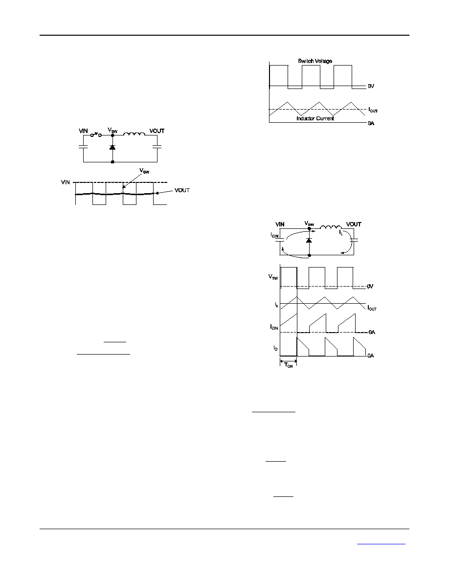
The MIC2208 is a 3A PWM non-synchronous
buck regulator.
By switching an input voltage
supply, and filtering the switched voltage through an
Inductor and capacitor, a regulated DC voltage is
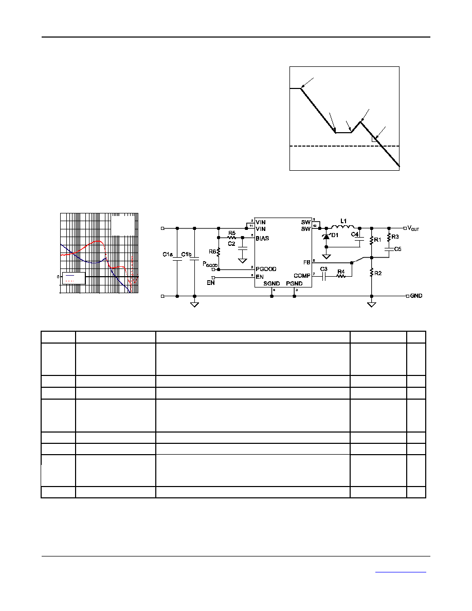
obtained. Figure 1 shows a simplified example of a
non-synchronous buck converter.
Figure 1.
For a non-synchronous buck converter, there are
two modes of operation; continuous and
discontinuous. Continuous or discontinuous refer to
the inductor current. If current is continuously flowing
through the inductor throughout the switching cycle,
it is in continuous operation. If the inductor current
drops to zero during the off time, it is in
discontinuous operation. Critically continuous is the
point where any decrease in output current will
cause it to enter discontinuous operation. The
critically continuous load current can be calculated
as follows;
L
2
1MHz
V
V
-
V
I
IN
2
OUT
OUT
OUT
◊
◊
=
Continuous or discontinuous operation determines
how we calculate peak inductor current.
Continuous Operation
Figure 2 illustrates the switch voltage and inductor
current during continuous operation.
Figure 2. Continuous Operation
The output voltage is regulated by pulse width
modulating (PWM) the switch voltage to the average
required output voltage. The switching can be
broken up into two cycles; On and Off.
During the on-time,
the high side switch is turned
on, current flows from the input supply through the
inductor and to the output. The inductor current is
Figure 3. On-Time
charged at the rate;
(
)
L
V
V
OUT
IN
-
To determine the total on-time, or time at which the
inductor charges, the duty cycle needs to be
calculated. The duty cycle can be calculated as;
IN
OUT
V
V
D
=
and the On time is;
1MHz
D
T
ON
=
September 2005
9
M9999-092905
www.micrel.com

Micrel, Inc.
MIC2208
Therefore, peak to peak ripple current is;
(
)
L
1MHz
V
V
V
-
V
I
IN
OUT
OUT
IN
pk
pk
◊
◊
=
-
Since the average peak-to-peak current is equal to
the load current. The actual peak (or highest current
the inductor will see in a steady state condition) is
equal to the output current plus half the peak-to-
peak current. For those of you who have not had
enough formulas already, here it is;
(
)
L
1MHz
2
V
V
V
-
V
I
I
IN
OUT
OUT
IN
OUT
pk
◊
◊
◊
+
=
Figure 4 demonstrates the off-time.
During the off-
time, the high-side internal P-channel MOSFET
turns off. Since the current in the inductor has to
discharge, the current flows through the free-
wheeling Schottky diode to the output. In this case,
the inductor discharge rate is (where V
D
is the diode
forward voltage);
(
)
L
V
V
D
OUT
+
-
The total off time can be calculated as;
1MHz
D
-
1
T
OFF
=
Figure 4. Off-Time
Discontinuous Operation
Discontinuous operation is when the inductor current
discharges to zero during the off cycle. Figure 5.
demonstrates the switch voltage and inductor
currents during discontinuous operation.
Figure 5. Discontinuous Operation
When the inductor current (I
L
) has completely
discharged, the voltage on the switch node rings at
the frequency determined by the parasitic
capacitance and the inductor value. In Figure 5, it is
drawn as a DC voltage, but to see actual operation
(with ringing and all) refer to the functional
characteristics.
Discontinuous mode of operation has the advantage
over full PWM in that at light loads, the MIC2208 will
skip pulses as nessasary, reducing gate drive
losses, drastically improving light load efficiency.
Efficiency Considerations
Calculating the efficiency is as simple as measuring
power out and dividing it by the power in;
100
P
P
Efficiency
IN
OUT
◊
=
Where input power (P
IN
) is;
IN
IN
IN
I
V
P
◊
=
and output power (P
OUT
) is calculated as;
OUT
OUT
OUT
I
V
P
◊
=
The Efficiency of the MIC2208 is determined by
several factors.
∑ Rdson (Internal P-channel Resistance)
∑ Diode conduction losses
∑ Inductor Conduction losses
∑ Switching losses
Rdson losses
are caused by the current flowing
through the high side P-channel MOSFET. The
amount of power loss can be approximated by;
September 2005
10
M9999-092905
www.micrel.com

Micrel, Inc.
MIC2208
D
I
R
P
2
OUT
DSON
SW
◊
◊
=
Where D is the duty cycle.
Since the MIC2208 uses an internal P-channel
MOSFET, Rdson losses are inversely proportional to
supply voltage. Higher supply voltage yields a higher
gate to source voltage, reducing the Rdson,
reducing the MOSFET conduction losses. A graph
showing typical Rdson vs input supply voltage can
be found in the typical characteristics section of this
datasheet.
Diode conduction losses
occur due to the forward
voltage drop (V
F
) and the output current. Diode
power losses can be approximated as follows:
(
)
D
1
I
V
P
OUT
F
D
-
◊
◊
=
For this reason, the Schottky diode is the rectifier of
choice. Using the lowest forward voltage drop will
help reduce diode conduction losses, and improve
efficiency.
Duty cycle, or the ratio of output voltage-to-input
voltage, determines whether the dominant factor in
conduction losses will be the internal MOSFET or
the Schottky diode. Higher duty cycles place the
power losses on the high side switch, and lower duty
cycles place the power losses on the schottky diode.
Inductor conduction losses
(P
L
) can be calculated
by multiplying the DC resistance (DCR) times the
square of the output current;
2
OUT
L
I
DCR
P
◊
=
Also, be aware that there are additional core losses
associated with switching current in an inductor.
Since most inductor manufacturers do not give data
on the type of material used, approximating core
losses becomes very difficult, so verify inductor
temperature rise.
Switching losses occur twice each cycle
, when
the switch turns on and when the switch turns off.
This is caused by a non-ideal world where switching
transitions are not instantaneous, and neither are
currents. Figure 6 demonstrates (Or exaggerates.)
how switching losses due to the transitions dissipate
power in the switch.
Figure 6. Switching Transition Losses
Normally, when the switch is on, the voltage across
the switch is low (virtually zero) and the current
through the switch is high. This equates to low
power dissipation. When the switch is off, voltage
across the switch is high and the current is zero,
again with power dissipation being low. During the
transitions, the voltage across the switch (V
S-D
) and
the current through the switch (I
S-D
) are at middle,
causing the transition to be the highest
instantaneous power point. During continuous mode,
these losses are the highest. Also, with higher load
currents, these losses are higher. For discontinuous
operation, the transition losses only occur during the
"off" transition since the "on" transitions there is no
current flow through the inductor.
Component Selection
Input Capacitor
A 10
µF ceramic is recommended on each VIN pin
for bypassing. X5R or X7R dielectrics are
recommended for the input capacitor. Y5V
dielectrics lose most of their capacitance over
temperature and are therefore, not recommended.
Also, tantalum and electrolytic capacitors alone are
not recommended due their reduced RMS current
handling, reliability, and ESR increases.
An additional 0.1
µF is recommended close to the
VIN and PGND pins for high frequency filtering.
Smaller case size capacitors are recommended due
to their lower ESR and ESL. Please refer to layout
recommendations for proper layout of the input
capacitor.
Inductor Selection
The MIC2208 is designed for use with a 1
µH
inductor. Proper selection should ensure the
inductor can handle the maximum average and peak
currents required by the load. Maximum current
ratings of the inductor are generally given in two
methods; permissible DC current and saturation
current. Permissible DC current can be rated either
September 2005
11
M9999-092905
www.micrel.com

Micrel, Inc.
MIC2208
for a 40∞C temperature rise or a 10% to 20% loss in
inductance. Ensure the inductor selected can handle
the maximum operating current. When saturation
current is specified, make sure that there is enough
margin that the peak current will not saturate the
inductor.
20dB/Decade
Dominan
t
Pole
Zero
LC
Frequency
Gain (dB)
Diode Selection
Since the MIC2208 is non-synchronous, a free-
wheeling diode is required for proper operation. A
schottky diode is recommended due to the low
forward voltage drop and their fast reverse recovery
time. The diode should be rated to be able to handle
the average output current. Also, the reverse voltage
rating of the diode should exceed the maximum
input voltage. The lower the forward voltage drop of
the diode the better the efficiency. Please refer to
the layout recommendations to minimize switching
noise.
Compensation
The MIC2208 utilizes voltage mode compensation
and has the error amplifier pin (COMP) pinned out to
allow it to be compensated using external
components. This allows the MIC2208 to be stable
with a wide range of inductor and capacitor values.
Feedback Resistors
The feedback resistor set the output voltage by
dividing down the output and sending it to the
feedback pin. The feedback voltage is 1.0V.
Calculating the set output voltage is as follows;
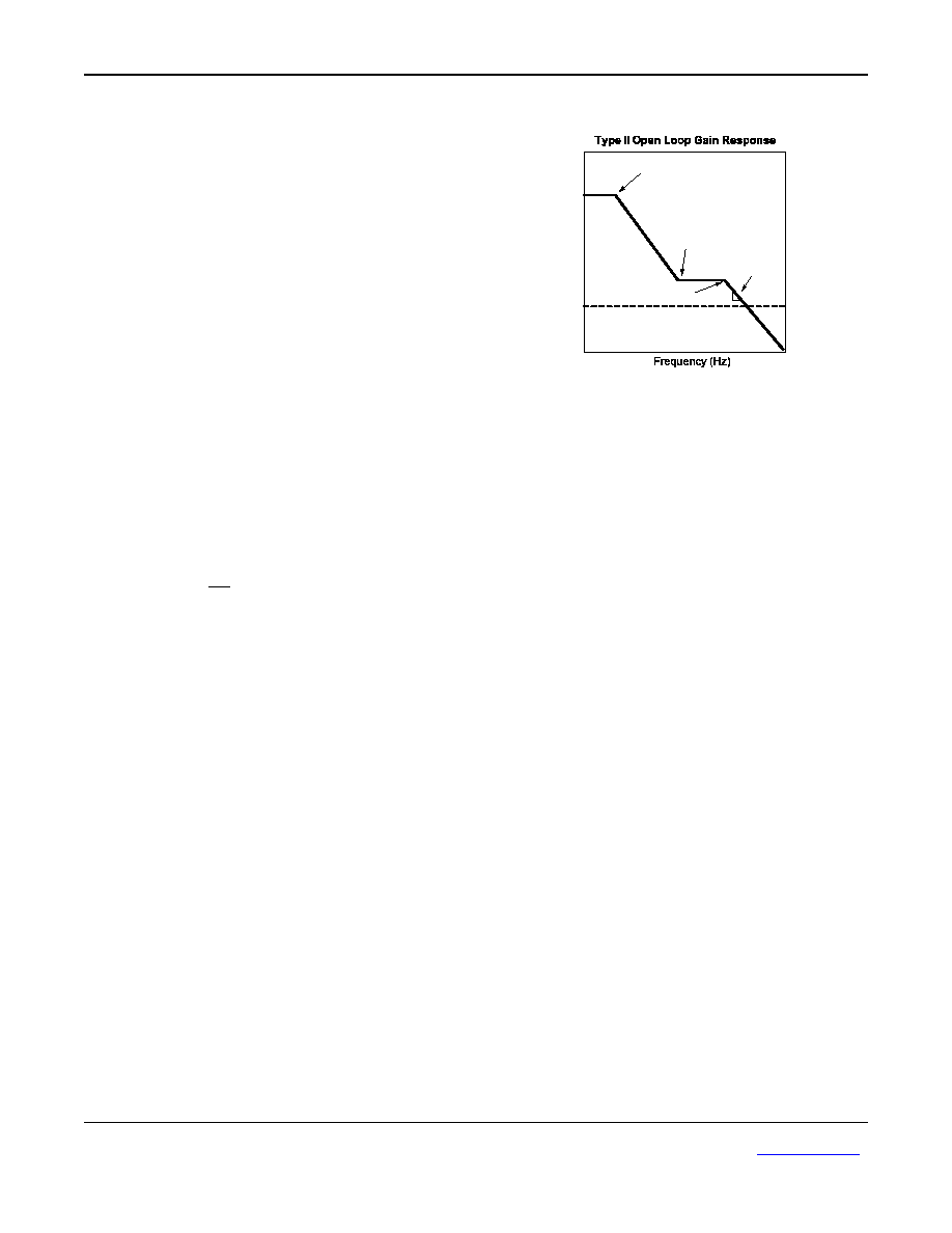
TYPE II compensation
Type II compensation can be expressed as pole-
zero-pole. In our case, a dominant pole (R1 and C3)
followed by a zero (C3 and R4) , allowing the final
pole to be provided by the output inductor and
output capacitor (L and C
OUT
). This mode of
compensation works well when using higher ESR
output capacitors, such as tantalum and electrolytic
dielectrics. The ESR of the capacitor, along with the
output capacitance provides a zero (C
OUT
and ESR)
that negates one of the two poles created by the
inductor-output capacitor filter. This allows the gain
to cross the 0dB point with a -1 slope
+
=
1
R2
R1
V
V
FB
OUT
Where R1 is the resistor from VOUT to FB and R2 is
the resistor from FB to GND. The recommended
feedback resistor values for common output
voltages is available in the bill of materials on page
x. Although the range of resistance for the FB
resistors is very wide, R1 is recommended to be
10K. This minimizes the effect the parasitic
capacitance of the FB node.
(-20dB/decade).
Bias filter
A small 10 Ohm resistor is recommended from the
input supply to the bias pin along with a small 0.1uF
ceramic capacitor from bias-to-ground. This will
bypass the high frequency noise generated by the
violent switching of high currents from reaching the
internal reference and control circuitry. Tantalum
and electrolytic capacitors are not recommended for
the bias, these types of capacitors lose their ability
to filter at high frequencies.
September 2005
12
M9999-092905
www.micrel.com

Micrel, Inc.
MIC2208
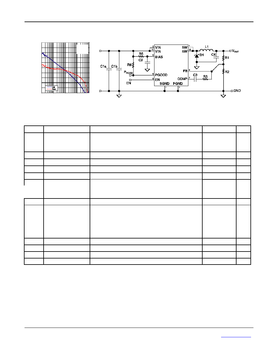
-20
-10
0
10
20
30
40
50
60
70
80
100
1k
10k
100k
1M
Frequency (KHz)
Type II Compensation
Ga
i
n
(
d
B
)
-72
-36
0
36
72
108
144
180
216
252
288
V
IN
=5V
IN
V
OUT
=1.0V
I
OUT
=3A
MIC2208
Bill of Materials
Item Part
Number
Description
Manufacturer Qty
C2012JB0J106K
10uF Ceramic Capacitor X5R 0805 6.3V
TDK
GRM219R60J106KE19 10uF Ceramic Capacitor X5R 0805 6.3V
Murata
C1a,C1b
08056D106MAT
10uF Ceramic Capacitor X5R 0805 6.3V
AVX
2
C2
0402ZD104MAT
0.1uF Ceramic Capacitor X5R 0402 10V
AVX
1
C3
0402ZD100MAT
100pF Ceramic Capacitor X5R 0402 10V
AVX
1
C4
TPME477M010R0030
470uF Tantalum Capacitor 10V
AVX
1
D1
SSA33L
3A Schottky 30V SMA
Vishay Semi
1
L1
RLF7030-1R0N6R4
1uH Inductor 8.8mOhm 7.1mm(L) x 6.8mm (W)x 3.2mm(H) TDK
744 778 9001
1uH Inductor 12mOhm 7.3mm(L)x7.3mm(W)x3.2mm(H)
Wurth Electronik
IHLP2525AH-01 1
1uH Inductor 17.5m
(L)6.47mmx(W)6.86mmx(H) 1.8mm
Vishay Dale
1
R1
CRCW04023012F 30.1K
1% 0402 resistor
Vishay Dale
1
CRCW04022002F
20 k
1% 0402 For 2.5V
OUT
Vishay Dale
CRCW04023742F
37.4 k
1% 0402 For 1.8 V
OUT
Vishay Dale
CRCW04026042F
60.4 k
1% 0402 For 1.5 V
OUT
Vishay Dale
CRCW04021503F
150 k
1% 0402 For 1.2 V
OUT
Vishay Dale
R2
Open For 1.0 V
OUT
Vishay
Dale
1
R4
CRCW04024993F 499K
1% 0402 resistor
Vishay Dale
1
R5
CRCW040210R0F 10
1% 0402 resistor
Vishay Dale
1
R6
CRCW04021002F 10K
1% 0402 resistor
Vishay Dale
1
U1
MIC2208BML
1MHz 3A Buck Regulator
Micrel
1
September 2005
13
M9999-092905
www.micrel.com

Micrel, Inc.
MIC2208
TYPE III compensation
Type III in our case, is a dominant pole (C3 and R1)
followed by a zero (C3 and R4) and an additional
zero (C5 and R4), allowing the final pole to be
provided by the output inductor and output capacitor.
This mode of compensation is required when using
low ESR output capacitors, such as ceramic
capacitors. The additional zero offsets the double
pole created by the inductor/output capacitor filter.
20dB/Decade
Dominant
Pole
Zero
LC
Frequency
Frequency (Hz)
Gai
n
(
d
B
)
Zero
Type III Open Loop Gain Response
-20
-10
10
20
30
40
50
60
70
80
100
1k
10k
100k
1M
Frequency (KHz)
Type III Compensation
Ga
in
(
d
B)
-72
-36
0
36
72
108
144
180
216
252
288
Gain
Phase
V
IN
=5V
IN
V
OUT
=1.0V
I
OUT
=3A
C
OUT
=47µF
MIC2208
Bill of Materials
Item Part
Number
Description
Manufacturer
Qty
C2012JB0J106K
10uF Ceramic Capacitor X5R 0805 6.3V
TDK
GRM219R60J106KE19 10uF Ceramic Capacitor X5R 0805 6.3V
Murata
C1a,C1b
08056D106MAT
10uF Ceramic Capacitor X5R 0805 6.3V
AVX
2
C2
0402ZD104MAT
0.1uF Ceramic Capacitor X5R 0402 10V
AVX
1
C3
0402ZD103MAT
1nF Ceramic Capacitor X5R 0402 10V
AVX
2
C3216X5R0J476K
47uF Ceramic Capacitor X5R 1206 6.3V
TDK
GRM32ER60J476ME20 47uF Ceramic Capacitor X5R 1206 6.3V
Murata
C4
12106D476MAT2A
47uF Ceramic Capacitor X5R 1210 6.3V
AVX
1
C5
VJ0402A330KXAA
33pF Ceramic Capacitor 0402
Vishay VT
1
D1
SSA33L
3A Schottky 30V SMA
Vishay Semi
1
L1
RLF7030-1R0N6R4
1uH Inductor 8.8mOhm 7.1mm(L) x 6.8mm (W)x 3.2mm(H)
TDK
744 778 9001
1uH Inductor 12mOhm 7.3mm(L)x7.3mm(W)x3.2mm(H)
Wurth Electronik
IHLP2525AH-01 1
1uH Inductor 17.5m
(L)6.47mmx(W)6.86mmx(H) 1.8mm
Vishay Dale
1
R1 CRCW04024992F 49.9K
1% 0402 resistor
Vishay Dale
1
September 2005
14
M9999-092905
www.micrel.com

Micrel, Inc.
MIC2208
Bill of Materials (cont.)
CRCW04023322F
33.2 k
1% 0402 For 2.5V
OUT
Vishay Dale
CRCW04026192F
61.9 k
1% 0402 For 1.8 V
OUT
Vishay Dale
CRCW04021003F
100 k
1% 0402 For 1.5 V
OUT
Vishay Dale
CRCW04022493F
249 k
1% 0402 For 1.2 V
OUT
Vishay Dale
R2
Open For 1.0 V
OUT
Vishay
Dale
1
R3 CRCW04024991F
4.99K
1% 0402 resistor
Vishay Dale
1
R4 CRCW04024991F
90.9K
1% 0402 resistor
Vishay Dale
1
R5 CRCW040210R0F
10
1% 0402 resistor
Vishay Dale
1
R6 CRCW04021002F
10K
1% 0402 resistor
Vishay Dale
1
U1
MIC2208BML
1MHz 3A Buck Regulator
Micrel
1
Loop Stability and Bode Analysis
Bode analysis is an excellent way to measure small
signal stability and loop response in power supply
designs. Bode analysis monitors gain and phase of
a control loop. This is done by breaking the
feedback loop and injecting a signal into the
feedback node and comparing the injected signal to
the output signal of the control loop. This will require
a network analyzer to sweep the frequency and
compare the injected signal to the output signal. The
most common method of injection is the use of
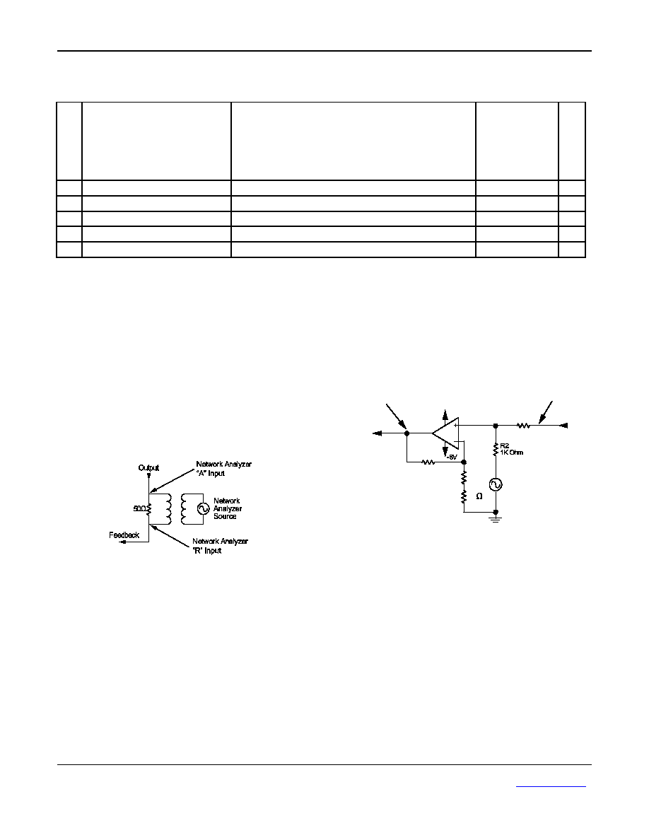
transformer. Figure 7 demonstrates how a
transformer is used to inject a signal into the
feedback network.
Figure 7. Transformer Injection
A 50 ohm resistor allows impedance matching from
the network analyzer source. This method allows the
DC loop to maintain regulation and allow the
network analyzer to insert an AC signal on top of the
DC voltage. The network analyzer will then sweep
the source while monitoring A and R for an A/R
measurement. While this is the most common
method for measuring the gain and phase of a
power supply, it does have significant limitations.
First, to measure low frequency gain and phase, the
transformer needs to be high in inductance. This
makes frequencies <100Hz require an extremely
large and expensive transformer. Conversely, it must
be able to inject high frequencies. Transformers with
these wide frequency ranges generally need to be
custom made and are extremely expensive (usually
in the tune of several hundred dollars!). By using an
op-amp, cost and frequency limitations used by an
injection transformer are completely eliminated.
Figure 8 demonstrates using an op-amp in a
summing amplifier configuration for signal injection.
Network Analyzer
Source
+8V
R1
1k
R3
1k
R4
1k
50
Feedback
Output
Network
Analyzer
"A" Input
Network
Analyzer
"R" Input
MIC922BC5
Figure 8. Op Amp Injection
R1 and R2 reduce the DC voltage from the output to
the non-inverting input by half. The network analyzer
is generally a 50 Ohm source. R1 and R2 also divide
the AC signal sourced by the network analyzer by
half. These two signals are "summed" together at
half of their original input. The output is then gained
up by 2 by R3 and R4 (the 50 Ohm is to balance the
network analyzer's source impedance) and sent to
the feedback signal. This essentially breaks the loop
and injects the AC signal on top of the DC output
voltage and sends it to the feedback. By monitoring
the feedback "R" and output "A", gain and phase are
measured. This method has no minimum frequency.
Ensure that the bandwidth of the op-amp being used
is much greater than the expected bandwidth of the
power supplies control loop. An op-amp with
September 2005
15
M9999-092905
www.micrel.com

Micrel, Inc.
MIC2208
>100MHz bandwidth is more than sufficient for most
power supplies (which includes both linear and
switching) and are more common and significantly
cheaper than the injection transformers previously
mentioned. The one disadvantage to using the op-
amp injection method, that the supply voltages need
to below the maximum operating voltage of the op-
amp. Also, the maximum output voltage for driving
50 Ohm inputs using the MIC922 is 3V. For
measuring higher output voltages, a 1MOhm input
impedance is required for the A and R channels.
Remember to always measure the output voltage
with an oscilloscope to ensure the measurement is
working properly. You should see a single sweeping
sinusoidal waveform without distortion on the output.
If there is distortion of the sinusoid, reduce the
amplitude of the source signal. You could be
overdriving the feedback causing a large signal
response.
Output Impedance and Transient
response
Output impedance, simply stated, is the amount of
output voltage deviation vs. the load current
deviation. The lower the output impedance, the
better.
OUT
OUT
OUT
I
V
Z
=
Output impedance for a buck regulator is the parallel
impedance of the output capacitor and the MOSFET
and inductor divided by the gain;
COUT
L
DSON
TOTAL
X
GAIN
X
DCR
R
Z
+
+
=
To measure output impedance vs. frequency, the
load current must be load current must be swept
across the frequencies measured, while the output
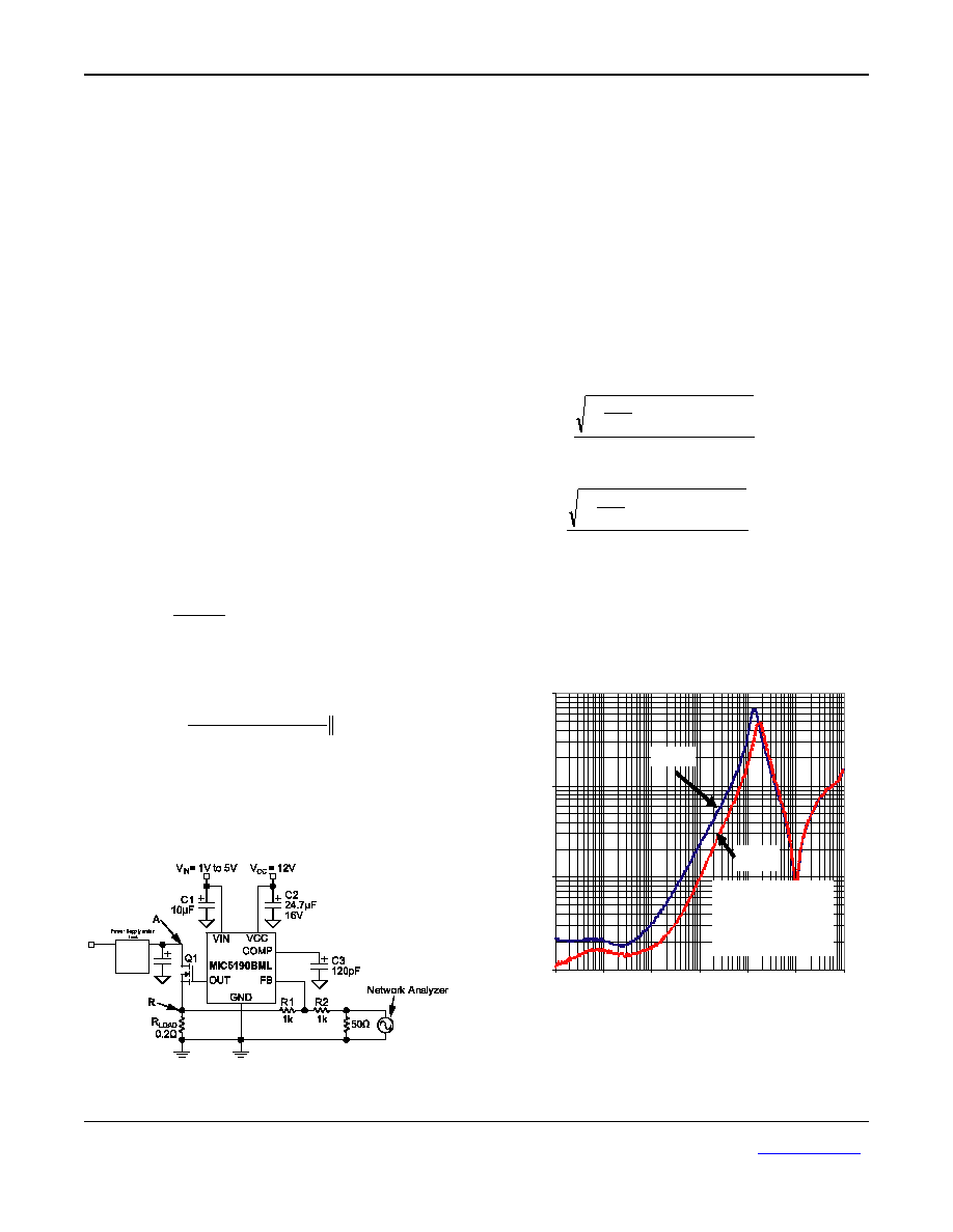
voltage is monitored. Figure 9 shows a test set-up to
measure output impedance from 10Hz to 1MHz
using the MIC5190 high speed controller.
Figure 9. Output Impedance Measurement
By setting up a network analyzer to sweep the
feedback current, while monitoring the output of the
voltage regulator and the voltage across the load
resistance, output impedance is easily obtainable.
To keep the current from being too high, a DC offset
needs to be applied to the network analyzer's source
signal. This can be done with an external supply and
50 Ohm resistor. Make sure that the currents are
verified with an oscilloscope first, to ensure the
integrity of the signal measurement. It is always a
good idea to monitor the A and R measurements
with a scope while you are sweeping it. To convert
the network analyzer data from dBm to something
more useful (such as peak-to-peak voltage and
current in our case);
707
.
0
2
50
1mW
10
V
10
dBm
◊
◊
◊
=
and peak to peak current;
LOAD
10
dBm
R
707
.
0
2
50
1mW
10
I
◊
◊
◊
◊
=
The following graph shows output impedance vs
frequency at 2A load current sweeping the AC
current from 10Hz to 10MHz, at 1A peak to peak
amplitude.
Output Impedance vs Frequency
0. 001
0. 01
0. 1
1
10
10 0
1k
10 k
10 0 k
1M
10 M
Frequency (Hz)
Ou
t
p
ut
I
mp
ed
an
c
e
(O
h
ms)
3.3V
IN
5V
IN
V
OUT
= 1.8V
L =1µH
C
OUT
= 4.7µF+0.1µF
From this graph, you can see the effects of
bandwidth and output capacitance. For frequencies
<100KHz, the output impedance is dominated by the
gain and inductance. For frequencies >100KHz, the
September 2005
16
M9999-092905
www.micrel.com

Micrel, Inc.
MIC2208
output impedance is dominated by the capacitance.
A good approximation for transient response can be
calculated from determining the frequency of the
load step in amps per second;
2
A/sec
=
f
Then, determine the output impedance by looking at
the output impedance vs frequency graph. Then
calculating the voltage deviation times the load step;
OUT
OUT
OUT
Z
I
V
◊
=
The output impedance graph shows the relationship
between supply voltage and output impedance. This
is caused by the lower Rdson of the high side
MOSFET and the increase in gain with increased
supply voltages. This explains why higher supply
voltages have better transient response.
COUT
L
DSON
TOTAL
X
GAIN
X
DCR
R
Z
+
+
=
Ripple measurements
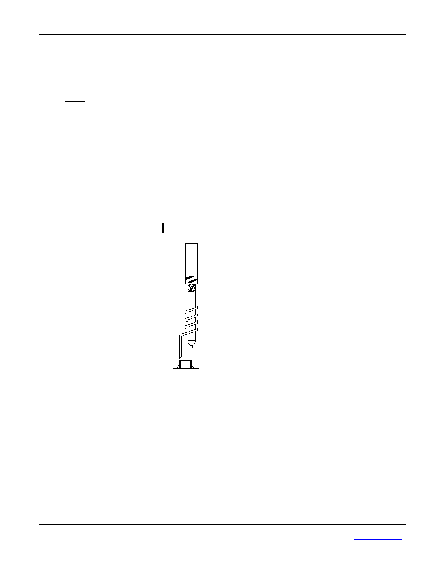
To properly measure ripple on either
input or output of a switching regulator,
a proper ring in tip measurement is required.
Standard oscilloscope probes come with a
grounding clip, or a long wire with an alligator clip.
Unfortunately, for high frequency measurements,
this ground clip can pick-up high frequency noise
and erroneously inject it into the measured output
ripple.
The standard evaluation board accommodates a
home made version by providing probe points for
both the input and output supplies and their
respective grounds. This requires the removing of
the oscilloscope probe sheath and ground clip from
a standard oscilloscope probe and wrapping a non-
shielded bus wire around the oscilloscope probe. If
there does not happen to be any non shielded bus
wire immediately available, the leads from axial
resistors will work. By maintaining the shortest
possible ground lengths on the oscilloscope probe,
true ripple measurements can be obtained.
September 2005
17
M9999-092905
www.micrel.com

Micrel, Inc.
MIC2208
September 2005
18
M9999-092905
www.micrel.com
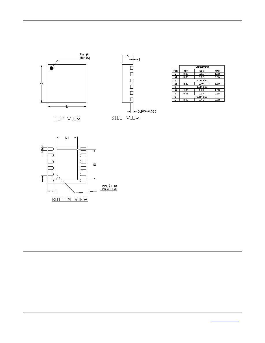
Package Information
12-Lead MLFTM (ML)
MICREL, INC. 2180 FORTUNE DRIVE SAN JOSE, CA 95131 USA
TEL +1 (408) 944-0800 FAX +1 (408) 474-1000 WEB http:/www.micrel.com
The information furnished by Micrel in this data sheet is believed to be accurate and reliable. However, no responsibility is assumed by Micrel
for its use. Micrel reserves the right to change circuitry and specifications at any time without notification to the customer.
Micrel Products are not designed or authorized for use as components in life support appliances, devices or systems where malfunction of a
product can reasonably be expected to result in personal injury. Life support devices or systems are devices or systems that (a) are intended
for surgical implant into the body or (b) support or sustain life, and whose failure to perform can be reasonably expected to result in a
significant injury to the user. A Purchaser's use or sale of Micrel Products for use in life support appliances, devices or systems is a
Purchaser's own risk and Purchaser agrees to fully indemnify Micrel for any damages resulting from such use or sale.
© 2005 Micrel, Incorporated.

Micrel, Inc.
MIC2208
Revision History
Date
Edits by:
Revision Number
3-30-05 Martin
Galinski
6-16-05
Martin Galinski
September 2005
19
M9999-092905
www.micrel.com


