August, 2004
1
M9999-081104
MIC2289
Micrel
MIC2289
2mm
◊◊
◊◊
◊
2mm White LED Driver
with Internal Schottky Diode and OVP
General Description
The MIC2289 is a PWM (pulse width modulated), boost-
switching regulator that is optimized for constant-current
white LED driver applications. The MIC2289 features an
internal Schottky diode and three levels of output overvoltage
protection providing a small size and efficient DC/DC solution
that requires only four external components.
To optimize efficiency, the feedback voltage is set to only
95mV. This reduces power dissipation in the current set
resistor and allows the lowest total output voltage, hence
minimal current draw from the battery.
The MIC2289 implements a constant frequency 1.2MHz
PWM control scheme. The high frequency, PWM operation
saves board space by reducing external component sizes.
The added benefit of the constant frequency PWM scheme in
caparison to varible frequency is much lower noise and input
ripple injected to the input power source.
The MIC2289 clamps the output voltage in case of open LED
conditions, protecting itself and the output capacitor. The
MIC2289 is available with three output OVP options of 15V,
24V, and 34V. The different OVP options allows the use of
the smallest possible output capacitor with the appropriate
voltage rating for a given application.
The MIC2289 is available in a 2mm
◊
2mm 8-pin MLFTM
package and has a junction temperature range of ≠40
∞
C to
+125
∞
C.
All support documentation can be found on Micrel's web
site at www.micrel.com.
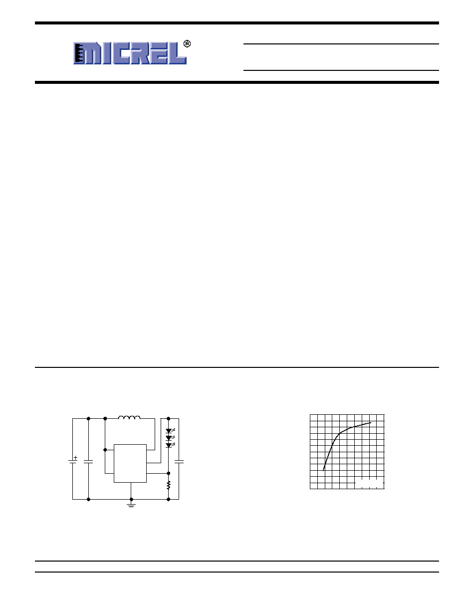
Typical Application
10
µ
H
0.22
µ
F/16V
6.3
95mV
1-Cell
Li Ion
1
µ
F
MIC2289-15BML
VIN
EN
SW
FB
OUT
GND
3-Series White LED Driver
Features
∑ 2.5V to 10V input voltage
∑ Output voltage up to 34V
∑ Internal Schottky diode
∑ 15V, 24V, 34V output OVP options
∑ 1.2 MHz PWM operation
∑ Over 500mA switch current
∑ 95mV feedback voltage
∑ <1% line and load regulation
∑ <1mA shutdown current
∑ Overtemperature protection
∑ UVLO
∑ 2mm
◊
2mm 8-pin MLFTM package
∑ ≠40
∞
C to +125
∞
C junction temperature range
Applications
∑ White LED driver for backlighting
Cell phones
PDAs
GPS systems
Digital cameras
MP3 players
IP phones
∑ LED flashlights
∑ Constant current power supplies
Micrel, Inc. ∑ 1849 Fortune Drive ∑ San Jose, CA 95131 ∑ USA ∑ tel + 1 (408) 944-0800 ∑ fax + 1 (408) 474-1000 ∑ http://www.micrel.com
Micro
LeadFrame and MLF are trademarks of Amkor Technology, Inc.
70
72
74
76
78
80
82
0
5
10
15
20
25
EFFICIENCY (%)
I
OUT
(mA)
3-Series LED Efficiency
V
IN
=3.6V
MIC2289
Micrel
M9999-081104
2
August, 2004
Pin Configuration
OUT
VIN
EN
AGND
PGND
SW
FB
NC
1
2
3
4
8
7
6
5
EP
MLFTM-8 (BML)
(Top View)
Fused Lead Frame
Ordering Information
Marking
Overvoltage
Junction
Part Number
Code
Protection
Temp. Range
Package
Lead Finish
MIC2289-15BML
SNA
15V
≠40
∞
C to 125
∞
C
2mm
◊
2mm MLFTM-8
Standard
MIC2289-15YML
SNA
15V
≠40
∞
C to 125
∞
C
2mm
◊
2mm MLFTM-8
Lead Free
MIC2289-24BML
SNB
24V
≠40
∞
C to 125
∞
C
2mm
◊
2mm MLFTM-8
Standard
MIC2289-24YML
SNB
24V
≠40
∞
C to 125
∞
C
2mm
◊
2mm MLFTM-8
Lead Free
MIC2289-34BML
SNC
34V
≠40
∞
C to 125
∞
C
2mm
◊
2mm MLFTM-8
Standard
MIC2289-34YML
SNC
34V
≠40
∞
C to 125
∞
C
2mm
◊
2mm MLFTM-8
Lead Free
Pin Description
Pin Number
Pin Name
Pin Function
1
OUT
Output Pin and Overvoltage Protection (Output): Connect to the output
capacitor and LEDs
2
VIN
Supply (Input): Input voltage.
3
EN
Enable (Input): Logic high enables regulator, logic low shuts down regulator.
5
NC
No connect (no internal connection to die).
6
FB
Feedback (Input): Output voltage sense node. Connect the cathode of the
LED to this pin. A resistor from this pin to ground sets the LED current.
7
SW
Switch Node (Input): Internal power transistor collector.
4,8
GND
Ground (Return): Ground.
EP
GND
Ground (Return): Backside pad.

August, 2004
3
M9999-081104
MIC2289
Micrel
Absolute Maximum Ratings
(1)
Supply Voltage (V
IN
) ..................................................... 12V
Switch Voltage (V
SW
) ..................................... ≠0.3V to 34V
Enable Pin Voltage (V
EN
) ................................... ≠0.3 to V
IN
FB Voltage (V
FB
) ............................................................. 6V
Switch Current (I
SW
) ....................................................... 2A
Ambient Storage Temperature (T
S
) ......... ≠65
∞
C to +150
∞
C
Schottky Reverse Voltage (V
DA
) ................................... 34V
ESD Rating
(3)
................................................................ 2kV
Operating Ratings
(2)
Supply Voltage (V
IN
) ........................................ 2.5V to 10V
Output Voltage (V
OUT
) ..................................... V
IN
to V
OVP
Junction Temperature Range (T
J
) ........... ≠40
∞
C to +125
∞
C
Package Thermal Impedance
2mm
◊
2mmMLFTM-8 (
JA
) .................................. 93
∞
C/W
Electrical Characteristics
(4)
T
A
= 25
∞
C, V
IN
= V
EN
= 3.6V, V
OUT
= 10V, I
OUT
= 20mA, unless otherwise noted. Bold values indicate ≠40
∞
C
T
J
±
125
∞
C.
Symbol
Parameter
Condition
Min
Typ
Max
Units
V
IN
Supply Voltage Range
2.5
10
V
V
UVLO
Under Voltage Lockout
1.8
2.1
2.4
V
I
VIN
Quiescent Current
V
FB
> 200mV, (not switching)
2.5
5
mA
I
SD
Shutdown Current
V
EN
= 0V
(5)
0.1
1
µ
A
V
FB
Feedback Voltage
(
±
5%)
90
95
100
mV
I
FB
Feedback Input Current
V
FB
= 95mV
≠450
nA
Line Regulation
3V
V
IN
5V
0.5
1
%
Load Regulation
5mA
I
OUT
20mA
0.5
2
%
D
MAX
Maximum Duty Cycle
85
90
%
I
SW
Switch Current Limit
750
mA
V
SW
Switch Saturation Voltage
I
SW
= 0.5A
450
mV
I
SW
Switch Leakage Current
V
EN
= 0V, V
SW
= 10V
0.01
5
µ
A
V
EN
Enable Threshold
TURN ON
1.5
V
TURN OFF
0.4
V
I
EN
Enable Pin Current
V
EN
= 10V
20
40
µ
A
f
SW
Oscillator Frequency
1.05
1.2
1.35
MHz
V
D
Schottky Forward Drop
I
D
= 150mA
0.8
1
V
I
RD
Schottky Leakage Current
V
R
= 30V
4
µ
A
V
OVP
Overvoltage Protection
MIC2289-15
13
14
16
V
MIC2289-24
21
22.5
24
V
MIC2289-34
30
32
34
V
T
J
Overtemperature
150
∞
C
Threshold Shutdown
Hysteresis
10
∞
C
Notes:
1. Absolute maximum ratings indicate limits beyond which damage to the component may occur. Electrical specifications do not apply when operating
the device outside of its operating ratings. The maximum allowable power dissipation is a function of the maximum junction temperature, T
J
(max),
the junction-to-ambient thermal resistance,
JA
, and the ambient temperature, T
A
. The maximum allowable power dissipation will result in excessive
die temperature, and the regulator will go into thermal shutdown.
2. This device is not guaranteed to operate beyond its specified operating rating.
3. Devices are inherently ESD sensitive. Handling precautions required. Human body model.
4. Specification for packaged product only.
5. I
SD
= I
VIN
.
MIC2289
Micrel
M9999-081104
4
August, 2004
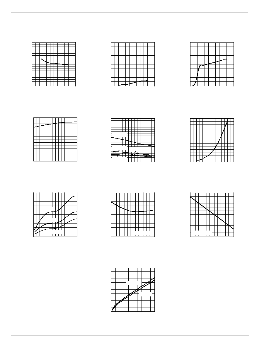
Typical Characteristics
90
91
92
93
94
95
96
97
98
99
100
0
2
4
6
8
10
12
FB VOLTAGE (mV)
V
IN
(V)
Feedback Voltage
vs. Input Voltage
0
1
2
3
4
5
0
2
4
6
8
10
12
SHUTDOWN CURRENT (
µ
A)
V
IN
(V)
Shutdown Current
vs. Input Voltage
0
1
2
3
4
5
0
2
4
6
8
10
12
QUIESCENT CURRENT (mA)
V
IN
(V)
Quiescent Current
vs. Input Voltage
0
0.2
0.4
0.6
0.8
1
1.2
1.4
-40 -20
0
20
40
60
80 100
SWITCHING FREQUENCY (MHz)
TEMPERATURE (
∞
C)
Switch Frequency
vs. Temperature
0
5
10
15
20
25
30
35
40
45
50
-50
0
50
100
IENABLE (
µ
A)
TEMPERATURE (
∞
C)
EN Pin Bias Current
vs. Temperature
I
EN
= 4.2V
I
EN
= 3.6V
I
EN
= 3.0V
I
EN
= 10V
0
100
200
300
400
500
600
700
450
550
650
750
850
950
1050
1150
SCHOTTKY FORWARD CURRENT (mA)
SCHOTTKY FORWARD VOLTAGE DROP (mV)
Schottky Forward
Voltage Drop
0
0.5
1
1.5
2
2.5
30
40
50
60
70
80
90 100
SCHOTTKY LEAKAGE CURRENT (
µ
A)
TEMPERATURE (
∞
C)
Schottky Reverse
Leakage Current
V
R
= 25V
V
R
= 10V
V
R
= 16V
300
350
400
450
500
550
-40
0
40
80
120
SATURATION VOLTAGE (mV)
TEMPERATURE (
∞
C)
Saturation Voltage
vs. Temperature
I
SW
= 500mA
600
650
700
750
800
850
900
-40
0
40
80
120
CURRENT LIMIT (mA)
TEMPERATURE (
∞
C)
Current Limit
vs. Temperature
V
IN
= 2.5V
0
100
200
300
400
500
600
0
100
200
300
400
500
SATURATION VOLTAGE (mV)
I
SW
(mA)
Switch Saturation Voltage
vs. Current
V
IN
= 2.5V
V
IN
= 5V
August, 2004
5
M9999-081104
MIC2289
Micrel
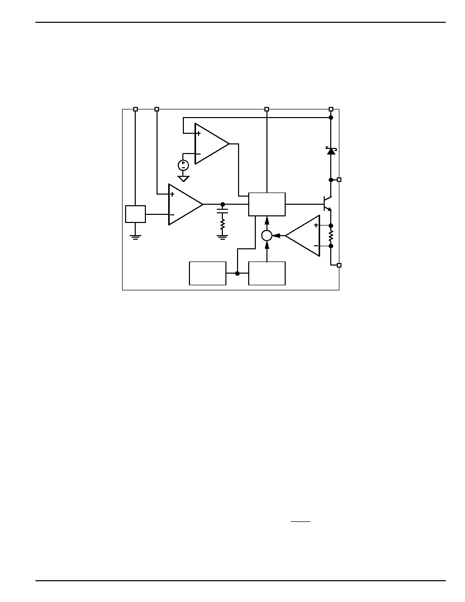
Functional Description
The MIC2289 is a constant frequency, PWM current mode
boost regulator. The block diagram is shown above. The
MIC2289 is composed of an oscillator, slope compensation
ramp generator, current amplifier, g
m
error amplifier, PWM
generator, 500mA bipolar output transistor, and Schottky
rectifier diode. The oscillator generates a 1.2MHz clock. The
clock's two functions are to trigger the PWM generator that
turns on the output transistor and to reset the slope compen-
sation ramp generator. The current amplifier is used to
measure the switch current by amplifying the voltage signal
from the internal sense resistor. The output of the current
amplifier is summed with the output of the slope compensa-
tion ramp generator. This summed current-loop signal is fed
to one of the inputs of the PWM generator.
Functional Diagram
GND
V
REF
PWM
Generator
Ramp
Generator
1.2MHz
Oscillator
SW
EN
FB
OUT
VIN
95mV
g
m
OVP
MIC2289 Block Diagram
The g
m
error amplifier measures the LED current through the
external sense resistor and amplifies the error between the
detected signal and the 95mV reference voltage. The output
of the g
m
error amplifier provides the voltage-loop signal that
is fed to the other input of the PWM generator. When the
current-loop signal exceeds the voltage-loop signal, the
PWM generator turns off the bipolar output transistor. The
next clock period initiates the next switching cycle, maintain-
ing the constant frequency current-mode PWM control. The
LED is set by the feedback resistor:
I
LED
=
95mv
R
FB
The Enable pin shuts down the output switching and disables
control circuitry to reduce input current to leakage levels.
Enable pin input current is zero at zero volts.

MIC2289
Micrel
M9999-081104
6
August, 2004
External Component Selection
The MIC2289 can be used across a wide rage of applications.
Series LEDs
L
Manufacturer
Min C
OUT
Manufacturer
2
22
µ
H
LQH32CN220K21 (Murata)
2.2
µ
F
0805ZD225KAT(AVX)
NLC453232T-220K(TDK)
GRM40X5R225K10(Murata)
15
µ
H
LQH32CN150K21 (Murata)
1
µ
F
0805ZD105KAT(AVX)
NLC453232T-150K(TDK)
GRM40X5R105K10(Murata)
10
µ
H
LQH32CN100K21 (Murata)
0.22
µ
F
0805ZD224KAT(AVX)
NLC453232T-100K(TDK)
GRM40X5R224K10(Murata)
6.8
µ
H
LQH32CN6R8K21 (Murata)
0.22
µ
F
0805ZD225KAT(AVX)
NLC453232T-6R8K(TDK)
GRM40X5R225K10(Murata)
4.7
µ
H
LQH32CN4R7K21 (Murata)
0.22
µ
F
0805ZD224KAT(AVX)
NLC453232T-4R7K(TDK)
GRM40X5R224K10(Murata)
3
22
µ
H
LQH43MN220K21 (Murata)
2.2
µ
F
0805YD225MAT(AVX)
NLC453232T-220K(TDK)
GRM40X5R225K16(Murata)
15
µ
H
LQH43MN 150K21 (Murata)
1
µ
F
0805YD105MAT(AVX)
NLC453232T-150K(TDK)
GRM40X5R105K16(Murata)
10
µ
H
LQH43MN 100K21 (Murata)
0.22
µ
F
0805YD224MAT(AVX)
NLC453232T-100K(TDK)
GRM40X5R224K16(Murata)
6.8
µ
H
LQH43MN 6R8K21 (Murata)
0.22
µ
F
0805YD224MAT(AVX)
NLC453232T-6R8K(TDK)
GRM40X5R224K16(Murata)
4.7
µ
H
LQH43MN 4R7K21 (Murata)
0.27
µ
F
0805YD274MAT(AVX)
NLC453232T-4R7K(TDK)
GRM40X5R224K16(Murata)
4
22
µ
H
LQH43MN220K21 (Murata)
1
µ
F
0805YD105MAT(AVX)
NLC453232T-220K(TDK)
GRM40X5R105K25(Murata)
15
µ
H
LQH43MN 150K21 (Murata)
1
µ
F
0805YD105MAT(AVX)
NLC453232T-150K(TDK)
GRM40X5R105K25(Murata)
10
µ
H
LQH43MN 100K21 (Murata)
0.27
µ
F
0805YD274MAT(AVX)
NLC453232T-100K(TDK)
GRM40X5R274K25(Murata)
6.8
µ
H
LQH43MN 6R8K21 (Murata)
0.27
µ
F
0805YD274MAT(AVX)
NLC453232T-6R8K(TDK)
GRM40X5R274K25(Murata)
4.7
µ
H
LQH43MN 4R7K21 (Murata)
0.27
µ
F
0805YD274MAT(AVX)
NLC453232T-4R7K(TDK)
GRM40X5R274K25(Murata)
5, 6
22
µ
H
LQH43MN220K21 (Murata)
0.22
µ
F
08053D224MAT(AVX)
NLC453232T-220K(TDK)
GRM40X5R224K25(Murata)
15
µ
H
LQH43MN 150K21 (Murata)
0.22
µ
F
08053D224MAT(AVX)
NLC453232T-150K(TDK)
GRM40X5R224K25(Murata)
10
µ
H
LQH43MN 100K21 (Murata)
0.27
µ
F
08053D274MAT(AVX)
NLC453232T-100K(TDK)
GRM40X5R274K25(Murata)
6.8
µ
H
LQH43MN 6R8K21 (Murata)
0.27
µ
F
08053D274MAT(AVX)
NLC453232T-6R8K(TDK)
GRM40X5R274K25(Murata)
4.7
µ
H
LQH43MN 4R7K21 (Murata)
0.27
µ
F
08053D274MAT(AVX)
NLC453232T-4R7K(TDK)
GRM40X5R274K25(Murata)
7, 8
22
µ
H
LQH43MN220K21 (Murata)
0.22
µ
F
08053D224MAT(AVX)
NLC453232T-220K(TDK)
GRM40X5R224K25(Murata)
15
µ
H
LQH43MN 150K21 (Murata)
0.22
µ
F
08053D224MAT(AVX)
NLC453232T-150K(TDK)
GRM40X5R224K25(Murata)
10
µ
H
LQH43MN 100K21 (Murata)
0.27
µ
F
08053D274MAT(AVX)
NLC453232T-100K(TDK)
GRM40X5R274K25(Murata)
6.8
µ
H
LQH43MN 6R8K21 (Murata)
0.27
µ
F
08053D274MAT(AVX)
NLC453232T-6R8K(TDK)
GRM40X5R274K25(Murata)
4.7
µ
H
LQH43MN 4R7K21 (Murata)
0.27
µ
F
08053D274MAT(AVX)
NLC453232T-4R7K(TDK)
GRM40X5R274K25(Murata)
The table below shows recommended inductor and output
capacitor values for various series-LED applications:
August, 2004
7
M9999-081104
MIC2289
Micrel
Dimming Control
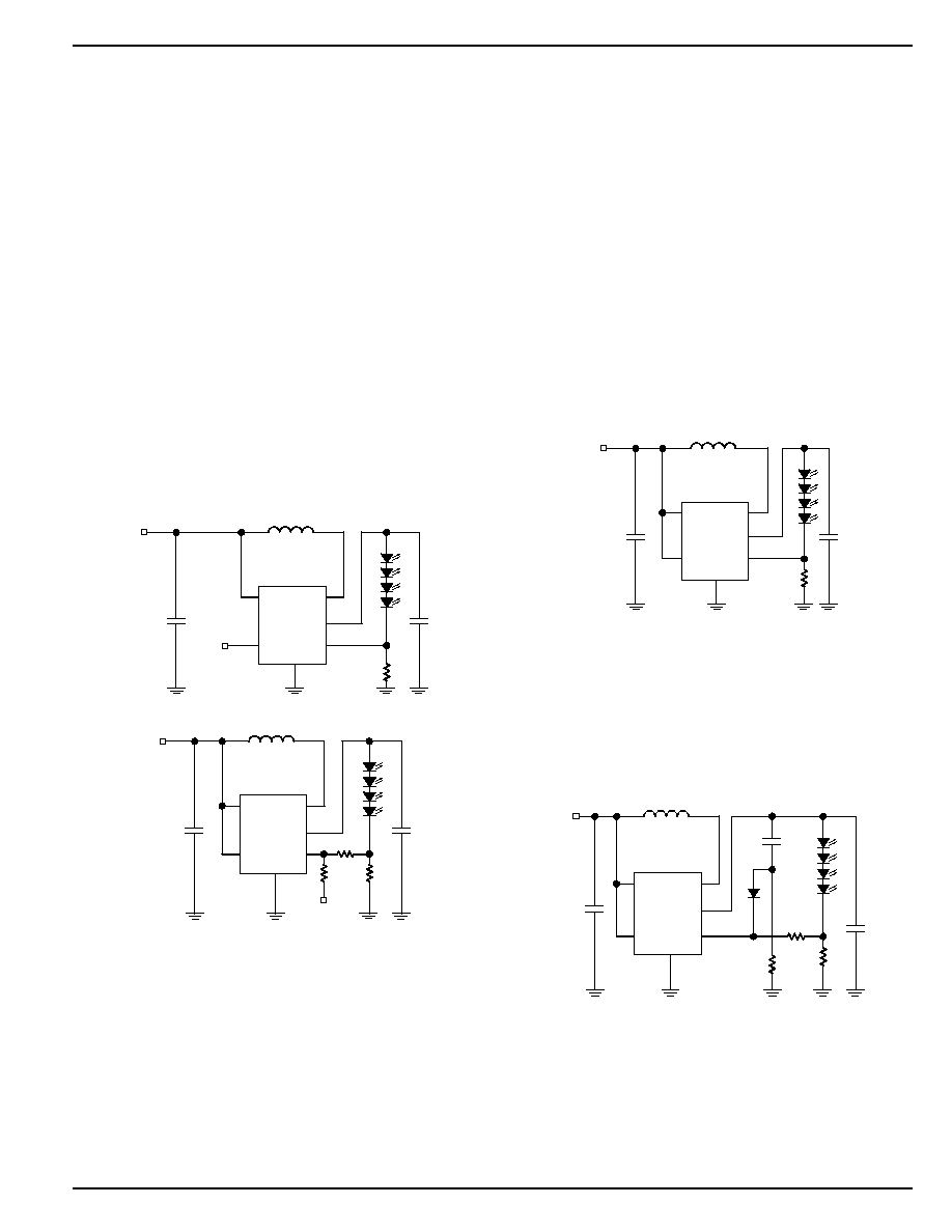
There are two techniques for dimming control. One is PWM
dimming, and the other is continuous dimming.
1. PWM dimming control is implemented by applying
a PWM signal on EN pin as shown in Figure 1. The
MIC2289 is turned on and off by the PWM signal.
With this method, the LEDs operate with either
zero or full current. The average LED current is
increased proportionally to the duty-cycle of the
PWM signal. This technique has high-efficiency
because the IC and the LEDs consume no current
during the off cycle of the PWM signal. Typical
frequency should be between 100Hz and 10kHz.
2. Continuous dimming control is implemented by
applying a DC control voltage to the FB pin of the
MIC2289 through a series resistor as shown in
Figure 2. The LED current is decreased propor-
tionally with the amplitude of the control voltage.
The LED intensity (current) can be dynamically
varied applying a DC voltage to the FB pin. The DC
voltage can come from a DAC signal, or a filtered
PWM signal . The advantage of this approach is
that a high frequency PWM signal (>10kHz) can be
used to control LED intensity.
PWM
VIN
EN
SW
FB
OUT
GND
V
IN
Figure 1. PWM Dimming Method
VIN
EN
SW
FB
OUT
5.11k
49.9k
GND
DC
Equivalent
V
IN
Figure 2. Continuous Dimming
Open-Circuit Protection
If the LEDs are disconnected from the circuit, or in case an
LED fails open, the sense resistor will pull the FB pin to
ground. This will cause the MIC2289 to switch with a high
duty-cycle, resulting in output overvoltage. This may cause
the SW pin voltage to exceed its maximum voltage rating,
possibly damaging the IC and the external components. To
ensure the highest level of protection, the MIC2289 has 3
product options in the 2mm
◊
2mm MLFTM-8 with overvoltage
protection, OVP. The extra pins of the 2mm
◊
2mm
MLFTM-8 package allow a dedicated OVP monitor with op-
tions for 15V, 24V, or 34V (see Figure 3). The reason for the
three OVP levels is to let users choose the suitable level of
OVP for their application. For example, a 3-LED application
would typically see an output voltage of no more than 12V, so
a 15V OVP option would offer a suitable level of protection.
This allows the user to select the output diode and capacitor
with the lowest voltage ratings, therefore smallest size and
lowest cost. The OVP will clamp the output voltage to within
the specified limits.
VIN
EN
GND
SW
FB
OUT
V
IN
Figure 3. MLFTM Package OVP Circuit
Start-Up and Inrush Current
During start-up, inrush current of approximately double the
nominal current flows to set up the inductor current and the
voltage on the output capacitor. If the inrush current needs to
be limited, a soft-start circuit similar to Figure 4 could be
implemented. The soft-start capacitor, C
SS
, provides over-
drive to the FB pin at start-up, resulting in gradual increase of
switch duty cycle and limited inrush current.
VIN
EN
10k
2200pF
SW
OUT
FB
C
SS
R
GND
V
IN
Figure 4. One of Soft-Start Circuit
MIC2289
Micrel
M9999-081104
8
August, 2004
6-Series LED Circuit without External Soft-Start
TIME (100
µ
s/div.)
ENABLE
(2V/div)
INPUT
CURRENT
(200mA/div)
OUTPUT
VOL
T
AGE
L = 10
µ
H
C
IN
= 1
µ
F
C
OUT
= 0.22
µ
F
V
IN
= 3.6V
I
OUT
= 20mA
6 LEDs
Figure 6. 6-Series LED Circuit
without External Soft-Start
6-Series LED Circuit with External Soft-Start
TIME (100
µ
s/div.)
ENABLE
(2V/div)
INPUT
CURRENT
(200mA/div)
OUTPUT
VOL
T
AGE
L = 10
µ
H
C
IN
= 1
µ
F
C
OUT
= 0.22
µ
F
V
IN
= 3.6V
I
OUT
= 20mA
6 LEDs
C
SS
= 2200pF
R = 10k
Figure 7. 6-Series LED Circuit
with External Soft-Start
August, 2004
9
M9999-081104
MIC2289
Micrel
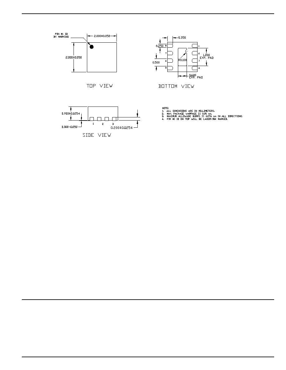
Package Information
8-Pin MLFTM (BML)
MICREL, INC.
1849 FORTUNE DRIVE
SAN JOSE, CA 95131
USA
TEL
+ 1 (408) 944-0800
FAX
+ 1 (408) 474-1000
WEB
http://www.micrel.com
The information furnished by Micrel in this data sheet is believed to be accurate and reliable. However, no responsibility is assumed by Micrel for its use.
Micrel reserves the right to change circuitry and specifications at any time without notification to the customer.
Micrel Products are not designed or authorized for use as components in life support appliances, devices or systems where malfunction of a product can
reasonably be expected to result in personal injury. Life support devices or systems are devices or systems that (a) are intended for surgical implant into
the body or (b) support or sustain life, and whose failure to perform can be reasonably expected to result in a significant injury to the user. A Purchaser's
use or sale of Micrel Products for use in life support appliances, devices or systems is at Purchaser's own risk and Purchaser agrees to fully indemnify
Micrel for any damages resulting from such use or sale.
© 2004 Micrel, Incorporated.