 | –≠–ª–µ–∫—Ç—Ä–æ–Ω–Ω—ã–π –∫–æ–º–ø–æ–Ω–µ–Ω—Ç: MIC2290 | –°–∫–∞—á–∞—Ç—å:  PDF PDF  ZIP ZIP |
August 2004
1
M9999-081104
MIC2290
Micrel
MIC2290
2mm
◊◊
◊◊
◊
2mm PWM Boost Regulator with
Internal Schotty Diode
General Description
The MIC2290 is a 1.2MHz , PWM, boost-switching regulator
housed in the small size 2mm
◊
2mm MLFTM-8 package. The
MIC2290 features an internal Schottky diode that reduces
circuit board area and total solution cost. High power density
is achieved with the MIC2290's internal 34V/0.5A switch,
allowing it to power large loads in a tiny footprint.
The MIC2290 implements a constant frequency 1.2MHz
PWM control scheme. The high frequency operation saves
board space by reducing external component sizes. The
fixed frequency PWM topology also reduces switching noise
and ripple to the input power source.
The MIC2290's wide 2.5V to 10V input voltage allows direct
operation from 3- to 4-cell NiCad/NiMH/Alkaline batteries, 1-
and 2-cell Li Ion batteries, as well as fixed 3.3V and 5V
systems.
The MIC2290 is available in a low-profile 2mm
◊
2mm
8-pin MLFTM leadless package and operates from a junction
temperature range of ≠40
∞
C to +125
∞
C.
All support documentation can be found on Micrel's web
site at www.micrel.com.
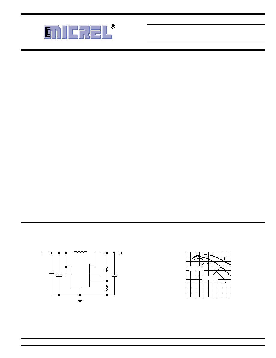
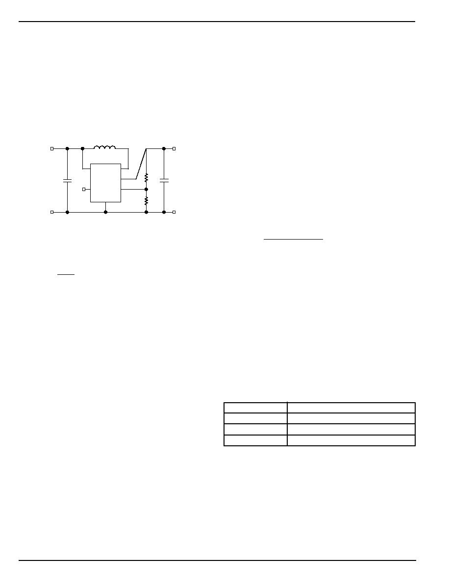
Typical Application
4, 8
L1
10
µ
H
R2
R1
1
7
3
2
MIC2290BML
VIN
Li Ion
Battery
V
OUT
12V
EN
SW
OUT
GND
V
IN
C1
1
µ
F
C2
10
µ
F
FB
6
Simple 12V Boost Regulator
Features
∑ Internal Schottky diode
∑ 2.5V to 10V input voltage
∑ Output voltage adjustable to 34V
∑ Over 500mA switch current
∑ 1.2MHz PWM operation
∑ Stable with ceramic capacitors
∑ <1% line and load regulation
∑ Low input and output ripple
∑ <1
µ
A shutdown current
∑ UVLO
∑ Output overvoltage protection
∑ Over temperature protection
∑ 2mm
◊
2mm 8-pin MLFTM package
∑ ≠40
∞
C to +125
∞
C junction temperature range
Applications
∑ Organic EL power supply
∑ TFT LCD bias supply
∑ 12V DSL power supply
∑ CCD bias supply
∑ SEPIC converters
Micrel, Inc. ∑ 1849 Fortune Drive ∑ San Jose, CA 95131 ∑ USA ∑ tel + 1 (408) 944-0800 ∑ fax + 1 (408) 474-1000 ∑ http://www.micrel.com
Micro
LeadFrame and MLF are trademarks of Amkor Technology, Inc.
60
65
70
75
80
85
0
0.02
0.04
0.06
0.08
0.1
EFFICIENCY (%)
LOAD CURRENT (A)
12V
OUT
Efficiency
V
IN
= 4.2V
V
IN
= 3.2V
V
IN
= 3.6V
MIC2290
Micrel
M9999-081104
2
August 2004
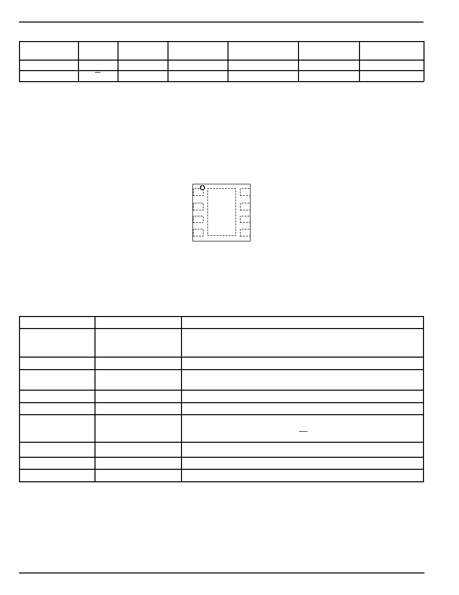
Pin Configuration
OUT
VIN
EN
AGND
PGND
SW
FB
NC
1
2
3
4
8
7
6
5
8-Pin MLFTM (ML)
(Top View)
Fused Lead Frame
Ordering Information
Marking
Output
Overvoltage
Junction
Part Number
Code
Voltage
Protection
Temp. Range
Package
Lead Finish
MIC2290BML
SRC
Adjustable
34V
≠40
∞
C to 125
∞
C
2
◊
2 8-pin MLFTM
Standard
MIC2290YML
SRC
Adjustable
34V
≠40
∞
C to 125
∞
C
2
◊
2 8-pin MLFTM
Lead Free
Pin Description
Pin Number
Pin Name
Pin Function
1
OUT
Output pin (Output): Output voltage. Connect to FB resistor divider. This pin
has an internal 34V output overvoltage clamp. See "Block Diagram" and
"Applications" section for more information.
2
VIN
Supply (Input): 2.5V to 10V input voltage.
3
EN
Enable (Input): Logic high enables regulator. Logic low shuts down regula-
tor.
4
AGND
Analog ground.
5
NC
No connect (no internal connection to die).
6
FB
Feedback (Input): Output voltage sense node. Connect feedback resistor
network to this pin. V
OUT
= 1.24V
1
R1
R2
+
7
SW
Switch node (Input): Internal power Bipolar collector.
8
PGND
Power ground.
EP
GND
Ground (Return): Exposed backside pad.
August 2004
3
M9999-081104
MIC2290
Micrel
Absolute Maximum Ratings
(1)
Supply Voltage (V
IN
) ..................................................... 12V
Switch Voltage (V
SW
) ..................................... ≠0.3V to 34V
Enable Pin Voltage (V
EN
) ................................... ≠0.3 to V
IN
FB Voltage (V
FB
) ............................................................. 6V
Switch Current (I
SW
) ....................................................... 2A
Storage Temperature (T
S
) ....................... ≠65
∞
C to +150
∞
C
ESD Rating
(3)
................................................................ 2kV
Operating Ratings
(2)
Supply Voltage (V
IN
) ........................................ 2.5V to 10V
Junction Temperature Range (T
J
) ........... ≠40
∞
C to +125
∞
C
Package Thermal Impedance
2mm
◊
2mm MLFTM (
JA
) .................................... 93
∞
C/W
Electrical Characteristics
(4)
T
A
= 25
∞
C, V
IN
= V
EN
= 3.6V, V
OUT
= 10V, I
OUT
= 20mA, unless otherwise noted. Bold values indicate ≠40
∞
C
T
J
±
125
∞
C.
Symbol
Parameter
Condition
Min
Typ
Max
Units
V
IN
Supply Voltage Range
2.5
10
V
V
UVLO
Undervoltage Lockout
1.8
2.1
2.4
V
I
VIN
Quiescent Current
V
FB
= 2V, (not switching)
2.5
5
mA
I
SD
Shutdown Current
V
EN
= 0V
(5)
0.2
1
µ
A
V
FB
Feedback Voltage
(
±
1%)
1.227
1.24
1.252
V
(
±
2%) (Over Temp)
1.215
1.265
V
I
FB
Feedback Input Current
V
FB
= 1.24V
≠450
nA
Line Regulation
3V
V
IN
5V
0.1
1
%
Load Regulation
5mA
I
OUT
20mA
0.2
1
%
D
MAX
Maximum Duty Cycle
85
90
%
I
SW
Switch Current Limit
0.75
A
V
SW
Switch Saturation Voltage
I
SW
= 0.5A
450
mV
I
SW
Switch Leakage Current
V
EN
= 0V, V
SW
= 10V
0.01
5
µ
A
V
EN
Enable Threshold
Turn on
1.5
V
Turn off
0.4
V
I
EN
Enable Pin Current
V
EN
= 10V
20
40
µ
A
f
SW
Oscillator Frequency
1.05
1.2
1.35
MHz
V
D
Schottky Forward Drop
I
D
= 150mA
0.8
1
V
I
RD
Schottky Leakage Current
V
R
= 30V
4
µ
A
V
OVP
Overvoltage Protection
(nominal voltage)
30
32
34
V
T
J
Overtemperature
150
∞
C
Threshold Shutdown
Hysteresis
10
∞
C
Notes:
1. Absolute maximum ratings indicate limits beyond which damage to the component may occur. Electrical specifications do not apply when operating
the device outside of its operating ratings. The maximum allowable power dissipation is a function of the maximum junction temperature, T
J
(max),
the junction-to-ambient thermal resistance,
JA
, and the ambient temperature, T
A
. The maximum allowable power dissipation will result in excessive
die temperature, and the regulator will go into thermal shutdown.
2. This device is not guaranteed to operate beyond its specified operating rating.
3. IC devices are inherently ESD sensitive. Handling precautions required. Human body model rating: 1.5K in series with 100pF.
4. Specification for packaged product only.
5. I
SD
= I
VIN
.

MIC2290
Micrel
M9999-081104
4
August 2004
Typical Characteristics
50
55
60
65
70
75
80
85
90
0
25
50
75
100
EFFICIENCY (%)
OUTPUT CURRENT (mA)
Efficiency at V
OUT
= 12V
V
IN
= 4.2V
V
IN
= 3.6V
V
IN
= 3.3V
11.9
11.92
11.94
11.96
11.98
12
12.02
12.04
12.06
12.08
12.1
0
20
40
60
80
OUTPUT VOLTAGE (V)
LOAD (mA)
Load Regulation
V
IN
=
3.6V
1.22
1.23
1.23
1.24
1.24
1.25
1.25
1.26
1.26
-40 -20 0
20 40 60 80 100 120
FEEDBACK VOLTAGE (V)
TEMPERATURE (
∞
C)
Feedback Voltage
vs. Temperature
0
0.1
0.2
0.3
0.4
0.5
0.6
0.7
0.8
0.9
2.5
4
5.5
7
8.5
10
CURRENT LIMIT (A)
SUPPLY VOLTAGE (V)
Current Limit
vs. Supply Voltage
0
0.2
0.4
0.6
0.8
1.0
-40 -20 0
20 40 60 80 100 120
CURRENT LIMIT (A)
TEMPERATURE (
∞
C)
Current Limit
vs. Temperature
450
460
470
480
490
500
510
520
530
540
2.5
4
5.5
7
8.5
10
SWITCH SATURATION VOLTAGE (mV)
SUPPLY VOLTAGE (V)
Switch Saturation
vs. Supply Voltage
I
SW
= 500mA
0
100
200
300
400
500
600
700
0
100
200
300
400
500
SWITCH SATURATION VOLTAGE (mV)
SWITCH CURRENT (mA)
Switch Saturation
vs. Current
V
IN
= 3.6V
0
100
200
300
400
500
600
700
-40 -20 0
20 40 60 80 100 120
SWITCH SATURATION VOLTAGE (mV)
TEMPERATURE (
∞
C)
Switch Saturation Voltage
vs. Temperature
V
IN
= 3.6V
I
SW
= 500mA
1
1.05
1.1
1.15
1.2
1.25
1.3
1.35
1.4
-40 -20 0
20 40 60 80 100 120
FREQUENCY (MHz)
TEMPERATURE (
∞
C)
Frequency
vs. Temperature
80
82
84
86
88
90
92
94
96
98
100
2.5
4
5.5
7
8.5
10
MAXIMUM DUTY CYCLE (%)
SUPPLY VOLTAGE (V)
Maximum Duty Cycle
vs. Supply Voltage
85
87
89
91
93
95
97
99
-40 -20 0
20 40 60 80 100 120
MAXIMUM DUTY CYCLE (%)
TEMPERATURE (
∞
C)
Maximum Duty Cycle
vs. Temperature
V
IN
= 3.6V
0
100
200
300
400
500
600
700
-40 -20 0
20 40 60 80 100 120
FEEDBACK CURRENT (nA)
TEMPERATURE (
∞
C)
FB Pin Current
vs. Temperature

August 2004
5
M9999-081104
MIC2290
Micrel
1.1
1.12
1.14
1.16
1.18
1.2
1.22
1.24
1.26
1.28
1.3
2.5
4
5.5
7
8.5
10
ENABLE THRESHOLD (V)
SUPPLY VOLTAGE (V)
Enable Threshold
vs. Supply Voltage
0
100
200
300
400
500
600
700
-40 -20 0
20 40 60 80 100 120
FEEDBACK CURRENT (nA)
TEMPERATURE (
∞
C)
Schottky Diode Leakage
vs. Temperature
V
R
= 15V
0
10
20
30
40
50
60
70
80
90
100
0
5
10
15
20
25
30
35
REVERSE CURRENT (nA)
REVERSE VOLTAGE (V)
Schottky Reverse Leakage
vs. Reverse Voltage
MIC2290
Micrel
M9999-081104
6
August 2004
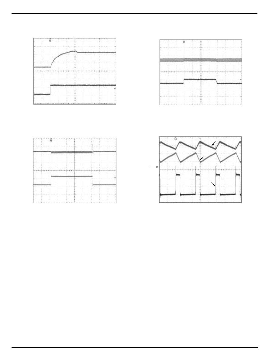
Function Characteristics
Enable Characteristics
Time (400µs/div)
OUTPUT
VOL
T
AGE
(5V/div)
ENABLE VOL
T
AGE
(2V/div)
3.6V
IN
12V
OUT
150mA Load
Line Transient Response
Time (400µs/div)
OUTPUT
VOL
T
AGE
(100mV/div) AC-Coupled
INPUT
VOL
T
A
GE
(2V/div)
12V
OUT
150mA Load
Load Transient Response
Time (400µs/div)
OUTPUT
VOL
T
AGE
(100mV/div) AC-Coupled
LOAD CURRENT
(50mA/div)
3.6V
IN
12V
OUT
C
OUT
= 10µF
Switching Waveforms
Time (400ns/div)
OUTPUT V
O
L
T
A
G
E
(50mV/div)
INDUCT
OR CURRENT
(500mA/div)
SWITCH SA
TURA
TION
(5V/div)
V
SW
Output Voltage
3.6V
IN
12V
OUT
60mA
Inductor Current
(10
µ
H)

August 2004
7
M9999-081104
MIC2290
Micrel
Functional Description
The MIC2290 is a constant frequency, PWM current mode
boost regulator. The block diagram is shown in Figure 1. The
MIC2290 is composed of an oscillator, slope compensation
ramp generator, current amplifier, g
m
error amplifier, PWM
generator, and a 0.5A bipolar output transistor. The oscillator
generates a 1.2MHz clock. The clock's two functions are to
trigger the PWM generator that turns on the output transistor,
and to reset the slope compensation ramp generator. The
current amplifier is used to measure the switch current by
amplifying the voltage signal from the internal sense resistor.
The output of the current amplifier is summed with the output
of the slope compensation ramp generator. This summed
current-loop signal is fed to one of the inputs of the PWM
generator.
Functional Diagram
GND
CA
V
REF
PWM
Generator
Ramp
Generator
1.2MHz
Oscillator
SW
EN
FB
OUT
VIN
1.24V
g
m
OVP
Figure 1. MIC2290 Block Diagram
The g
m
error amplifier measures the feedback voltage through
the external feedback resistors and amplifies the error be-
tween the detected signal and the 1.24V reference voltage.
The output of the g
m
error amplifier provides the voltage-loop
signal that is fed to the other input of the PWM generator.
When the current-loop signal exceeds the voltage-loop sig-
nal, the PWM generator turns off the bipolar output transistor.
The next clock period initiates the next switching cycle,
maintaining the constant frequency current-mode PWM con-
trol.
MIC2290
Micrel
M9999-081104
8
August 2004
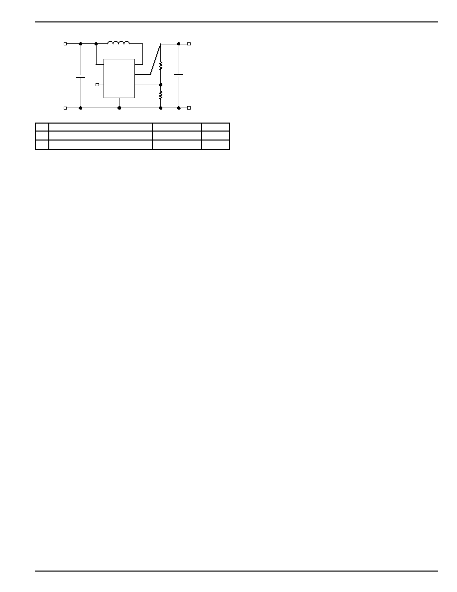
Applications Information
DC-to-DC PWM Boost Conversion
The MIC2290 is a constant frequency boost converter. It
operates by taking a DC input voltage and regulating a higher
DC output voltage. Figure 2 shows a typical circuit. Boost
regulation is achieved by turning on an internal switch, which
draws current through the inductor (L1). When the switch
turns off, the inductor's magnetic field collapses, causing the
current to be discharged into the output capacitor through an
internal Schottky diode (D1). Voltage regulation is achieved
through pulse-width modulation (PWM).
L1
10
µ
H
C2
10
µ
F
R2
R1
MIC2290BML
VIN
V
IN
V
OUT
EN
SW
FB
GND
GND
OUT
GND
C1
2.2
µ
F
Figure 2. Typical Application Circuit
Duty Cycle Considerations
Duty cycle refers to the switch on-to-off time ratio and can be
calculated as follows for a boost regulator:
D
1
V
V
IN
OUT
= -
The duty cycle required for voltage conversion should be less
than the maximum duty cycle of 85%. Also, in light load
conditions where the input voltage is close to the output
voltage, the minimum duty cycle can cause pulse skipping.
This is due to the energy stored in the inductor causing the
output to overshoot slightly over the regulated output voltage.
During the next cycle, the error amplifier detects the output as
being high and skips the following pulse. This effect can be
reduced by increasing the minimum load or by increasing the
inductor value. Increasing the inductor value reduces peak
current, which in turn reduces energy transfer in each cycle.
Overvoltage Protection
For the MLFTM package option, there is an overvoltage
protection function. If the feedback resistors are discon-
nected from the circuit or the feedback pin is shorted to
ground, the feedback pin will fall to ground potential. This will
cause the MIC2290 to switch at full duty cycle in an attempt
to maintain the feedback voltage. As a result, the output
voltage will climb out of control. This may cause the switch
node voltage to exceed its maximum voltage rating, possibly
damaging the IC and the external components. To ensure the
highest level of protection, the MIC2290 OVP pin will shut the
switch off when an overvoltage condition is detected, saving
itself and other sensitive circuitry downstream.
Component Selection
Inductor
Inductor selection is a balance between efficiency, stability,
cost, size, and rated current. For most applications, a 10
µ
H
is the recommended inductor value; it is usually a good
balance between these considerations.
Large inductance values reduce the peak-to-peak ripple
current, affecting efficiency. This has an effect of reducing
both the DC losses and the transition losses. There is also a
secondary effect of an inductor's DC resistance (DCR). The
DCR of an inductor will be higher for more inductance in the
same package size. This is due to the longer windings
required for an increase in inductance. Since the majority of
input current (minus the MIC2290 operating current) is passed
through the inductor, higher DCR inductors will reduce effi-
ciency.
To maintain stability, increasing inductor size will have to be
met with an increase in output capacitance. This is due to the
unavoidable "right half plane zero" effect for the continuous
current boost converter topology. The frequency at which the
right half plane zero occurs can be calculated as follows:
F
V
V
L I
2
rhpz
IN
OUT
OUT
=
◊ ◊
◊
2
The right half plane zero has the undesirable effect of
increasing gain, while decreasing phase. This requires that
the loop gain is rolled off before this has significant effect on
the total loop response. This can be accomplished by either
reducing inductance (increasing RHPZ frequency) or in-
creasing the output capacitor value (decreasing loop gain).
Output Capacitor
Output capacitor selection is also a trade-off between perfor-
mance, size, and cost. Increasing output capacitance will
lead to an improved transient response, but also an increase
in size and cost. X5R or X7R dielectric ceramic capacitors are
recommended for designs with the MIC2290. Y5V values
may be used, but to offset their tolerance over temperature,
more capacitance is required. The following table shows the
recommended ceramic (X5R) output capacitor value vs.
output voltage.
Output Voltage
Recomended Output Capacitance
<6V
22
µ
F
<16V
10
µ
F
<34V
4.7
µ
F
Table 1. Output Capacitor Selection
Input capacitor
A minimum 1
µ
F ceramic capacitor is recommended for
designing with the MIC2290. Increasing input capacitance
will improve performance and greater noise immunity on the
source. The input capacitor should be as close as possible to
the inductor and the MIC2290, with short traces for good
noise performance.

August 2004
9
M9999-081104
MIC2290
Micrel
Feedback Resistors
The MIC2290 utilizes a feedback pin to compare the output
to an internal reference. The output voltage is adjusted by
selecting the appropriate feedback resistor values. The de-
sired output voltage can be calculated as follows:
V
V
R1
R2
1
OUT
REF
=
◊
+
where V
REF
is equal to 1.24V.

MIC2290
Micrel
M9999-081104
10
August 2004
Application Circuits
L1
4.7
µ
H
C2
10
µ
F
6.3V
R2
100k
R1
5.62k
MIC2290BML
VIN
V
IN
3.3V
V
OUT
5V @ 180mA
EN
SW
FB
GND
GND
OUT
GND
C1
2.2
µ
F
6.3V
C1
2.2
µ
F, 6.3V, 0805 X5R Ceramic Capacitor
08056D475MAT
AVX
C2
10
µ
F, 6.3V, 0805 X5R Ceramic Capacitor
08056D106MAT
AVX
L1
4.7
µ
H, 450mA Inductor
LQH32CN4R7N11
Murata
Figure 3. 3.3V
IN
to 5V
OUT
@ 180mA
L1
10
µ
H
C2
10
µ
F
16V
R2
5k
R1
31.6k
MIC2290BML
VIN
V
IN
3V to 4.2V
V
OUT
9V @ 80mA
EN
SW
FB
GND
GND
OUT
GND
C1
2.2
µ
F
6.3V
C1
2.2
µ
F, 6.3V, 0603 X5R Ceramic Capacitor
06036D225MAT
AVX
C2
10
µ
F, 16V, 1206 X5R Ceramic Capacitor
1206YD106MAT
AVX
L1
10
µ
H, 450mA Inductor
LQH32CN100K11
Murata
Figure 4. 3.3V
IN
≠ 4.2V
IN
to 9V
OUT
@ 80mA
L1
10
µ
H
C2
10
µ
F
16V
R2
5k
R1
43.2k
MIC2290BML
VIN
V
IN
3V to 4.2V
V
OUT
12V @ 50mA
EN
SW
FB
GND
GND
OUT
GND
C1
2.2
µ
F
6.3V
C1
2.2
µ
F, 6.3V, 0603 X5R Ceramic Capacitor
06036D225MAT
AVX
C2
10
µ
F, 16V, 1206 X5R Ceramic Capacitor
1206YD106MAT
AVX
L1
10
µ
H, 450mA Inductor
LQH32CN100K11
Murata
Figure 5. 3.3V
IN
≠ 4.2V
IN
to 12V
OUT
@ 50mA
L1
10
µ
H
C2
10
µ
F
16V
R2
5k
R1
54.9k
MIC2290BML
VIN
V
IN
3V to 4.2V
V
OUT
15V @ 45mA
EN
SW
FB
GND
GND
OUT
GND
C1
2.2
µ
F
6.3V
C1
2.2
µ
F, 6.3V, 0603 X5R Ceramic Capacitor
06036D225MAT
AVX
C2
10
µ
F, 16V, 1206 X5R Ceramic Capacitor
1206YD106MAT
AVX
L1
10
µ
H, 450mA Inductor
LQH32CN100K11
Murata
Figure 6. 3.3V
IN
≠ 4.2V
IN
to 15V
OUT
@ 45mA
L1
10
µ
H
C2
10
µ
F
16V
R2
5k
R1
31.6k
MIC2290BML
VIN
V
IN
5V
V
OUT
9V @ 160mA
EN
SW
FB
GND
GND
OUT
GND
C1
2.2
µ
F
6.3V
C1
2.2
µ
F, 6.3V, 0603 X5R Ceramic Capacitor
06036D225MAT
AVX
C2
10
µ
F, 16V, 1206 X5R Ceramic Capacitor
1206YD106MAT
AVX
L1
10
µ
H, 450mA Inductor
LQH32CN100K11
Murata
Figure 7. 5V
IN
to 9V
OUT
@ 160mA
L1
10
µ
H
C2
10
µ
F
16V
R2
5k
R1
43.2k
MIC2290BML
VIN
V
IN
5V
V
OUT
12V @ 110mA
EN
SW
FB
GND
GND
OUT
GND
C1
2.2
µ
F
6.3V
C1
2.2
µ
F, 6.3V, 0603 X5R Ceramic Capacitor
06036D225MAT
AVX
C2
10
µ
F, 16V, 1206 X5R Ceramic Capacitor
1206YD106MAT
AVX
L1
10
µ
H, 450mA Inductor
LQH32CN100K11
Murata
Figure 8. 5V
IN
to 12V
OUT
@ 110mA
August 2004
11
M9999-081104
MIC2290
Micrel
L1
10
µ
H
C2
4.7
µ
F
25V
R2
1k
R1
18.2k
MIC2290BML
VIN
V
IN
5V
V
OUT
24V @ 40mA
EN
SW
FB
GND
GND
OUT
GND
C1
2.2
µ
F
6.3V
C1
2.2
µ
F, 6.3V, 0603 X5R Ceramic Capacitor
06036D225MAT
AVX
C2
4.7
µ
F, 25V, 1206 X5R Ceramic Capacitor
12063D475MAT
AVX
L1
10
µ
H, 450mA Inductor
LQH32CN100K11
Murata
Figure 9. 5V
IN
to 24V
OUT
@ 40mA
MIC2290
Micrel
M9999-081104
12
August 2004
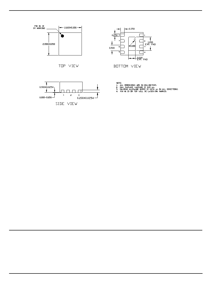
Package Information
8-Pin MLFTM (ML)
MICREL, INC.
1849 FORTUNE DRIVE
SAN JOSE, CA 95131
USA
TEL
+ 1 (408) 944-0800
FAX
+ 1 (408) 474-1000
WEB
http://www.micrel.com
The information furnished by Micrel in this data sheet is believed to be accurate and reliable. However, no responsibility is assumed by Micrel for its use.
Micrel reserves the right to change circuitry and specifications at any time without notification to the customer.
Micrel Products are not designed or authorized for use as components in life support appliances, devices or systems where malfunction of a product can
reasonably be expected to result in personal injury. Life support devices or systems are devices or systems that (a) are intended for surgical implant into
the body or (b) support or sustain life, and whose failure to perform can be reasonably expected to result in a significant injury to the user. A Purchaser's
use or sale of Micrel Products for use in life support appliances, devices or systems is at Purchaser's own risk and Purchaser agrees to fully indemnify
Micrel for any damages resulting from such use or sale.
© 2004 Micrel, Incorporated.