 | –≠–ª–µ–∫—Ç—Ä–æ–Ω–Ω—ã–π –∫–æ–º–ø–æ–Ω–µ–Ω—Ç: MIC2549A | –°–∫–∞—á–∞—Ç—å:  PDF PDF  ZIP ZIP |
December 2001
1
MIC2545A/2549A
MIC2545A/2549A
Micrel
MIC2545A/2549A
Programmable Current Limit High-Side Switch
Final Information
General Description
The MIC2545A and MIC2549A are integrated high-side
power switches optimized for low loss dc power switching and
other power management applications, including Advanced
Configuration and Power Interface (ACPI). The MIC2545A/
49A is a cost-effective, highly integrated solution that re-
quires few external components to satisfy USB and ACPI
requirements.
Load current management features include a precision resis-
tor-programmable output current-limit and a soft-start circuit,
which minimizes inrush current when the switch is enabled.
Thermal shutdown, along with adjustable current-limit, pro-
tects the switch and the attached device.
The MIC2545A/49A's open-drain flag output is used to indi-
cate current-limiting or thermal shutdown to a local controller.
The MIC2549A has an additional internal latch which turns
the output off upon thermal shutdown, providing robust fault
control. The enable signal is compatible with both 3V and 5V
logic, and is also used as the thermal shutdown latch reset for
the MIC2549A.
The MIC2545A and MIC2549A are available in active-high
and active-low enable versions in 8-pin DIP, SOIC, and
TSSOP packages.
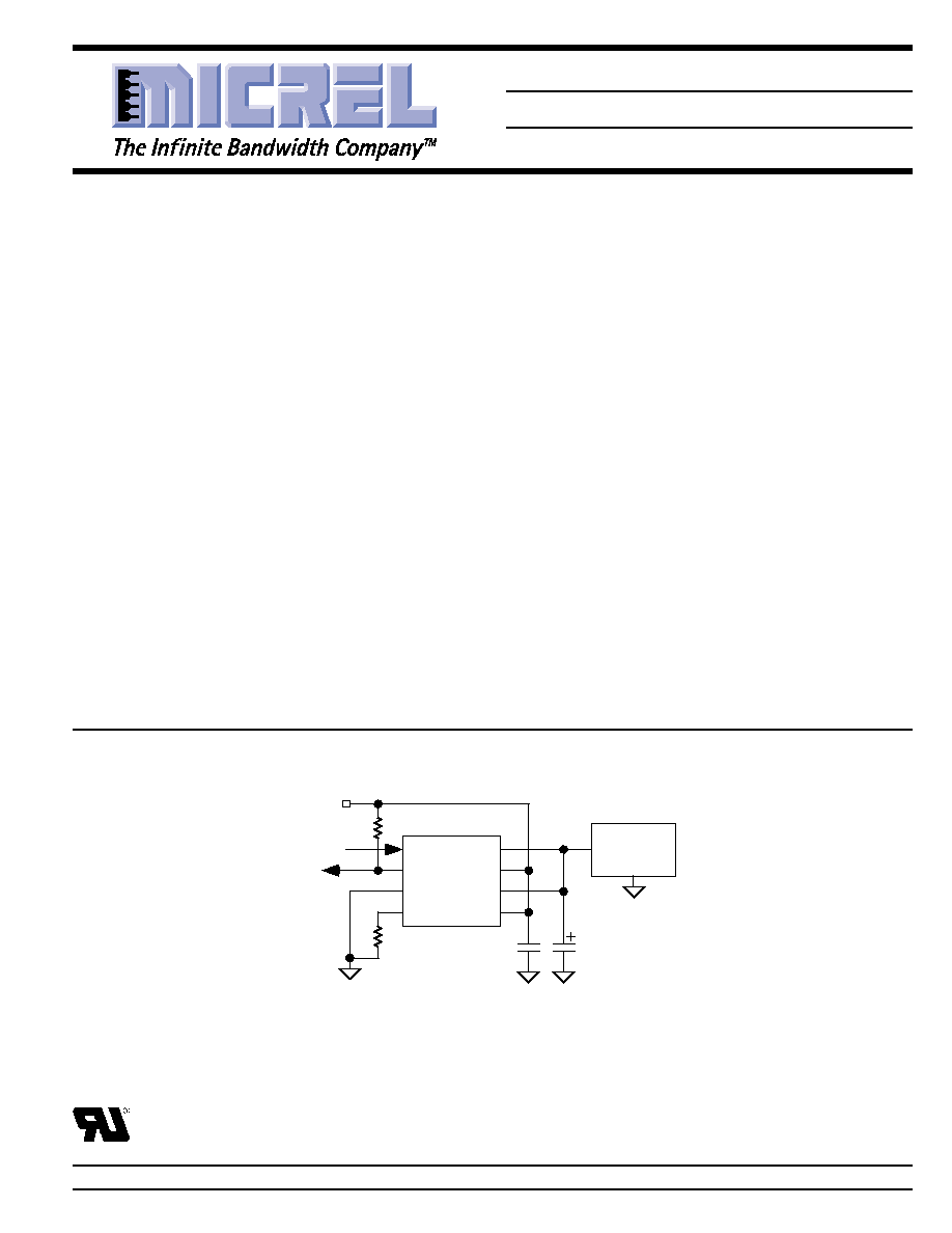
Typical Application
EN
FLG
GND
ILIM
OUT
IN
OUT
IN
MIC2545A
On/Off
Peripheral
0.1µF
R
SET
+5V
10k
33µF
Typical Advanced Configuration and Power Interface (ACPI) Application
Features
∑ 2.7V to 5.5V input
∑ Adjustable current-limit up to 3A
∑ Reverse current flow blocking
∑ 90
µ
A typical on-state supply current
∑ 1
µ
A typical off-state supply current
∑ 50m
maximum on-resistance
∑ Open-drain fault flag
∑ Thermal shutdown
∑ Thermal shutdown output latch (MIC2549A)
∑ 2ms (slow) soft-start turn-on, fast turnoff
∑ Available with active-high or active-low enable
Applications
∑ USB power distribution
∑ PCI Bus Power Switching
∑ Notebook PC
∑ ACPI power distribution
∑ PC card hot swap applications
∑ Inrush current-limiting
Micrel, Inc. ∑ 1849 Fortune Drive ∑ San Jose, CA 95131 ∑ USA ∑ tel + 1 (408) 944-0800 ∑ fax + 1 (408) 944-0970 ∑ http://www.micrel.com
UL Recognized Component

MIC2545A/2549A
Micrel
MIC2545A/2549A
2
December 2001
Pin Description
Pin Number
Pin Number
Pin Name
Pin Function
SOP, DIP
TSSOP
1
1
EN
Enable (Input): Logic-compatible enable input (-1 version is active high, -2
version is active low). High input >1.8V typical; low input <1.4V typical.
Do not float.
MIC2549A only: Also resets thermal shutdown latch.
2
3
FLG
Fault Flag (Output): Active-low, open-drain output. Indicates overcurrent or
thermal shutdown.
MIC2549A only: latched low on thermal shutdown.
3
5
GND
Ground: Supply return.
4
7
ILIM
Current Limit: Sets current limit threshold using an external resistor (R
SET
)
connected to ground. 76.8
< R
SET
< 459
.
5, 7
8, 12
IN
Supply Input: Output MOSFET drain. Also powers internal circuitry. Both IN
pins must be externally connected together.
6, 8
10, 14
OUT
Switch Output: Output MOSFET source. Both OUT pins must be externally
connected together.
2,4,6,9,11,13
NC
not internally connected
Pin Configuration
1
2
3
4
8
7
6
5
OUT
IN
OUT
IN
EN
FLG
GND
ILIM
MIC2545A/2549A
8-Lead SOP (M)
8-Pin DIP (N)
LOGIC,
CHARGE
PUMP
6,8 (OUT)
5,7 (IN)
(EN) 1
(FLG) 2
3 (GND)
(ILIM) 4
MIC2545A/2549A
Ordering Information
Part Number
Enable
Latch*
Temperature Range
Package
MIC2545A-1BM
Active High
≠40
∞
C to +85
∞
C
8-lead SOP
MIC2545A-1BN
Active High
≠40
∞
C to +85
∞
C
8-pin DIP
MIC2545A-1BTS
Active High
≠40
∞
C to +85
∞
C
14-lead TSSOP
MIC2545A-2BM
Active Low
≠40
∞
C to +85
∞
C
8-lead SOP
MIC2545A-2BN
Active Low
≠40
∞
C to +85
∞
C
8-pin DIP
MIC2545A-2BTS
Active Low
≠40
∞
C to +85
∞
C
14-lead TSSOP
MIC2549A-1BM
Active High
∑
≠40
∞
C to +85
∞
C
8-lead SOP
MIC2549A-1BN
Active High
∑
≠40
∞
C to +85
∞
C
8-pin DIP
MIC2549A-1BTS
Active High
∑
≠40
∞
C to +85
∞
C
14-lead TSSOP
MIC2549A-2BM
Active Low
∑
≠40
∞
C to +85
∞
C
8-lead SOP
MIC2549A-2BN
Active Low
∑
≠40
∞
C to +85
∞
C
8-pin DIP
MIC2549A-2BTS
Active Low
∑
≠40
∞
C to +85
∞
C
14-lead TSSOP
2
NC
3
FLG
4
NC
5
GND
6
NC
7
ILIM
1
EN
OUT
14
NC
13
IN
12
NC
11
OUT
10
NC
9
8
IN
MIC2545A/2549A
14-Lead TSSOP (TS)

December 2001
3
MIC2545A/2549A
MIC2545A/2549A
Micrel
Electrical Characteristics
V
IN
= +5V; T
A
= 25
∞
C, bold indicates ≠40
∞
C to +85
∞
C; unless noted
Symbol
Parameter
Condition
Min
Typ
Max
Units
Supply Current
Switch off, OUT = open, Note 4
0.75
5
µ
A
Switch on, OUT = open, Note 4
90
125
µ
A
150
µ
A
V
EN
Enable Input Voltage
Enable high transition, Note 4
2.4
1.6
V
Enable low transition, Note 1
1.5
0.8
V
Enable Input Current
V
EN
= V
OH(min)
= 2.4V
0.01
1
µ
A
V
EN
= V
OL(max)
= 0.8V
0.01
1
µ
A
Enable Input Capacitance
Note 7
1
pF
R
DS(on)
Switch Resistance
I
OUT
= 500mA
35
50
m
Current Limit Factor
I
LIMIT
= 0.5A to 3A, V
OUT
= 1V to 4V, Note 5
160
230
300
V
I
LIMIT
= 1A to 2.5A, V
OUT
= 1V to 4V, Note 5
184
230
276
V
Output Leakage Current
Switch off, V
OUT
= 0V
1
10
µ
A
t
ON
Output Turn-On Delay
R
L
= 10
, C
L
= 1
µ
F, Figures 1a, 1b
1
2
5
ms
t
R
Output Turn-On Rise Time
R
L
= 10
, C
L
= 1
µ
F, Figure 1a, 1b
0.75
1.8
4.9
ms
t
OFF
Output Turnoff Delay
R
L
= 10
, C
L
= 1
µ
F, Figure 1a, 1b
25
µ
s
t
F
Output Turnoff Fall Time
R
L
= 10
, C
L
= 1
µ
F, Figure 1a, 1b
23
µ
s
Overtemperature Threshold
T
J
increasing
135
∞
C
Shutdown
T
J
decreasing
120
∞
C
Error Flag Off Current
V
FLG
= 5V
0.01
1
µ
A
EN Pulse Reset Width
MIC2549A thermal shutdown latch, Note 7
1
µ
s
t
SU
V
IN
to EN Set-Up
MIC2549A, Note 7, Figure 1c
0
µ
s
Current-Limit Response Time
V
OUT
= 0V to I
OUT
= 2A, I
SET
= 1A, Note 7
40
µ
s
V
OL
Error Flag Output Resistance
I
FLG
= 10mA
4
15
Note 1.
Exceeding the absolute maximum rating may damage the device.
Note 2.
The device is not guaranteed to function outside its operating rating.
Note 3.
Devices are ESD sensitive. Handling precautions recommended. Human body model, 1.5k in series with 100pF.
Note 4.
Off is
0.8V and on is
2.4V for the MIC2545A-1 and MIC2549A-1. Off is
2.4V and on is
0.8V for the MIC2545A-2 and MIC2549A-2.
The enable input has about 100mV of hysteresis.
Note 5.
Current limit is determined by: I
R
LIMIT
SET
=
230
, where R
SET
is in ohms, and 230 is typical current limit factor in volts.
Note 6.
Assumes 4 layer PCB is used.
Note 7.
Guaranteed by design but not production tested.
Absolute Maximum Ratings
(Note 1)
Supply Voltage (V
IN
) .................................................. +7.0V
Output Voltage (V
OUT
) ............................................... +7.0V
Output Current (I
OUT
) ............................... Internally Limited
Enable Input (V
EN
) ......................................... ≠0.3V to +7V
Fault Flag Voltage (V
FLG
) ........................................... +7.0V
Fault Flag Current (I
FLG
) ............................................ 50mA
Storage Temperature (T
S
) ....................... ≠65
∞
C to +150
∞
C
Junction Temperature (T
J
) ....................... Internally Limited
Lead Temperature (soldering 5 sec.) ........................ 260
∞
C
ESD Rating, Note 3 .................................................. 2001V
Operating Ratings
(Note 2)
Supply Voltage (V
IN
) ................................... +2.7V to +5.5V
Ambient Temperature Range (T
A
) ............. ≠40
∞
C to +85
∞
C
Package Thermal Resistance
PDIP
(
JA
) ......................................................... 130
∞
C/W
SOIC
(
JA
) ......................................................... 160
∞
C/W
TSSOP
(
JA
), Note 6 ........................................ 100
∞
C/W
Current Limit Set Range, Note 5 ........................ 0.5A to 3A
MIC2545A/2549A
Micrel
MIC2545A/2549A
4
December 2001
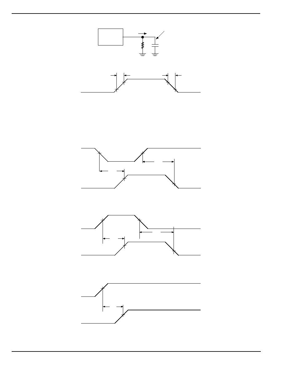
Test Circuit
Device
Under
Test
C
L
OUT
R
L
V
OUT
I
OUT
90%
V
OUT
10%
90%
10%
t
r
t
f
Functional Characteristics Test Circuit
Timing Diagrams
V
EN
50%
90%
V
OUT
10%
t
OFF
t
ON
Figure 1a. MIC2545A/49A-2
V
EN
50%
90%
V
OUT
10%
t
OFF
t
ON
Figure 1b. MIC2545A/49A-1
V
IN
V
EN
t
SU
Figure 1c. Input-to-Enable Setup Timing

December 2001
5
MIC2545A/2549A
MIC2545A/2549A
Micrel
EN
V
OUT
I
OUT
Short-Circuit Fault
Thermal Shutdown
Reached
FLG
I
LIMIT
I
DC
Output Reset
Fault Removed
Figure 2a. MIC2549A-2 Timing: Output Is Reset By Toggling EN
EN
V
OUT
I
OUT
Short-Circuit
Fault
Thermal Shutdown
Reached
Fault
Removed
FLG
I
LIMIT
I
DC
Figure 2b. MIC2545A-2 Timing

MIC2545A/2549A
Micrel
MIC2545A/2549A
6
December 2001
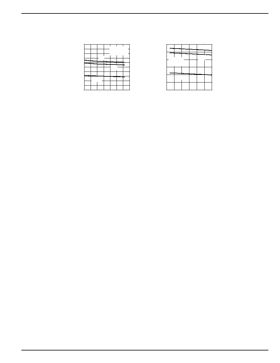
Typical Characteristics
30
31
32
33
34
35
36
37
38
39
40
2.5
3.0
3.5
4.0
4.5
5.0
5.5
OUTPUT RESISTANCE (m
)
SUPPLY VOLTAGE (V)
Output On-Resistance
vs. Supply Voltage
T
A
= 27
∞
C
25
30
35
40
45
50
-40 -20
0
20
40
60
80 100
OUTPUT RESISTANCE (m
)
TEMPERATURE (
∞
C)
Output On-Resistance
vs. Temperature
2.7V
3.3V
5.0V
0
20
40
60
80
100
120
140
2.5
3.0
3.5
4.0
4.5
5.0
5.5
SUPPLY CURRENT (
µ
A)
SUPPLY VOLTAGE (V)
On-State Supply Current
vs. Supply Voltage
T
A
= 27
∞
C
0
20
40
60
80
100
120
140
-40 -20
0
20
40
60
80 100
SUPPLY CURRENT (
µ
A)
TEMPERATURE (
∞
C)
On-State Supply Current
vs. Temperature
2.7V
3.3V
5.0V
0
0.1
0.2
0.3
0.4
0.5
-40 -20
0
20
40
60
80 100
SUPPLY CURRENT (
µ
A)
TEMPERATURE (
∞
C)
Off-State Supply Current
vs. Temperature
2.7V
3.3V
5.0V
R
L
= 44
0
0.01
0.02
0.03
0.04
0.05
0.06
0.07
0.08
0.09
0.10
2.5
3.0
3.5
4.0
4.5
5.0
5.5
SUPPLY CURRENT (
µ
A)
SUPPLY VOLTAGE (V)
Off-State Supply Current
vs. Supply Voltage
T
A
= 27
∞
C
1.0
1.1
1.2
1.3
1.4
1.5
1.6
1.7
1.8
1.9
2.0
2.5
3.0
3.5
4.0
4.5
5.0
5.5
THRESHOLD VOLATAGE (V)
SUPPLY VOLTAGE (V)
Control Threshold Voltage
vs. Supply Voltage
T
A
= 27
∞
C
HIGH
LOW
1.1
1.2
1.3
1.4
1.5
1.6
1.7
1.8
1.9
-40 -20
0
20
40
60
80 100
CONTROL THRESHOLD (V)
TEMPERATURE (
∞
C)
Control Threshold Voltage
vs. Temperature
LOW
HIGH
0
0.5
1.0
1.5
2.0
2.5
3.0
3.5
4.0
-40 -20
0
20
40
60
80 100
OUTPUT RISE TIME (ms)
TEMPERATURE (
∞
C)
Rise Time
vs. Temperature
2.7V
3.3V
5.0V
R
L
= 44
0
0.2
0.4
0.6
0.8
1.0
1.2
1.4
1.6
1.8
-40 -20
0
20
40
60
80 100
OUTPUT FALL TIME (
µ
s)
TEMPERATURE (
∞
C)
Output Fall Time
vs. Temperature
2.7V
3.3V
R
L
= 44
5.0V
C
L
= 0
µ
F
0
500
1000
1500
2000
2500
3000
3500
0
150
300
450
600
CURRENT LIMIT (mA)
R
SET
(
)
Current Limit
vs. Rset
I
TH
V
IN
= 5V
I
LIMIT
I
SHORT
0
500
1000
1500
2000
2500
3000
3500
0
1.0
2.0
3.0
4.0
5.0
6.0
OUTPUT CURRENT (mA)
OUTPUT VOLTAGE (V)
Output Current
vs. Output Voltage
R
SET
= 92
V
IN
= 5V
R
SET
= 230
R
SET
= 460
December 2001
7
MIC2545A/2549A
MIC2545A/2549A
Micrel
500
600
700
800
900
1000
1100
1200
1300
1400
1500
-40 -20
0
20
40
60
80 100
OUTPUT CURRENT (mA)
TEMPERATURE (
∞
C)
Current Limit
vs. Temperature
I
TH
I
SET
I
SHORT
V
IN
= 5V
R
SET
= 230
600
700
800
900
1000
1100
1200
2.5
3.0
3.5
4.0
4.5
5.0
5.5
CURRENT LIMIT (mA)
SUPPLY VOLTAGE (V)
Current Limit
vs. Supply Voltage
I
TH
I
SET
I
SHORT
T
A
= 27
∞
C
R
L
= 230

MIC2545A/2549A
Micrel
MIC2545A/2549A
8
December 2001
Functional Characteristics
Turn-On Response
TIME (500
µ
s/div.)
MIC2545A-1
I
OUT
(200mA/div
.
)
V
OUT
(2V/div
.
)
V
EN
(10V/div
.
)
V
FLG
(10V/div
.
)
500mA
V
IN
= 5V
C
L
= 100
µ
F
R
L
= 10
Turnoff Response
TIME (1ms/div.)
MIC2545A-1
V
IN
= 5V
C
L
= 100
µ
F
R
L
= 10
500mA
I
OUT
(200mA/div
.)
V
OUT
(2V/div
.)
V
EN
(10V/div
.)
V
FLG
(10V/div
.)
Current-Limit Response
TIME (100ms/div.)
MIC2545A-1
I
OUT
(500mA/div
.
)
V
OUT
(5V/div
.
)
V
EN
(10V/div
.
)
V
FLG
(10V/div
.
)
Load Removed
C = 5V
R
L
= 1
Current-Limit Threshold 1.12A (I
TH
)
I
SET
= 1A
Thermal Shutdown
Short-Circuit Response
TIME (100ms/div.)
I
OUT
(500mA/div
.
)
V
OUT
(5V/div
.
)
V
EN
(10V/div
.
)
V
FLG
(10V/div
.
)
MIC2545A-1
V
IN
= 5V
Short Circuit
Current-Limit Threshold 1.12A
Thermal
Shutdown
Short-Circuit Current
820mA (I
SHORT
)
Enable Into Short Circuit
TIME (100ms/div.)
MIC2545A-1
I
OUT
(500mA/div
.
)
V
OUT
(5V/div
.
)
V
EN
(10V/div
.
)
V
FLG
(10V/div
.
)
Short-Circuit Current
820mA
V
IN
= 5V
R
SET
= 240
Thermal
Shutdown
Inrush Current Response
TIME (500
µ
s/div.)
MIC2545A-1
V
IN
= 5V
R
L
= 10
I
OUT
(500mA/div
.
)
V
EN
(10V/div
.
)
V
FLG
(10V/div
.
)
C
L
= 10
µ
F
C
L
= 130
µ
F
C
L
= 490
µ
F
December 2001
9
MIC2545A/2549A
MIC2545A/2549A
Micrel
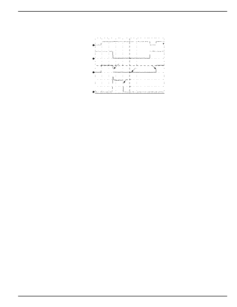
Thermal Shutdown
(Output Reset by Toggling Enable--MIC2549-1)
TIME (100ms/div.)
I
OUT
(500mA/div
.
)
V
EN
(10V/div
.
)
V
OUT
(5V/div
.
)
V
FLG
(5V/div
.
)
Thermal
Shutdown
Output Reset
Ramped Load to a Short
V
IN
= 5V
C
L
= 47
µ
F
Output Latched
MIC2545A/2549A
Micrel
MIC2545A/2549A
10
December 2001
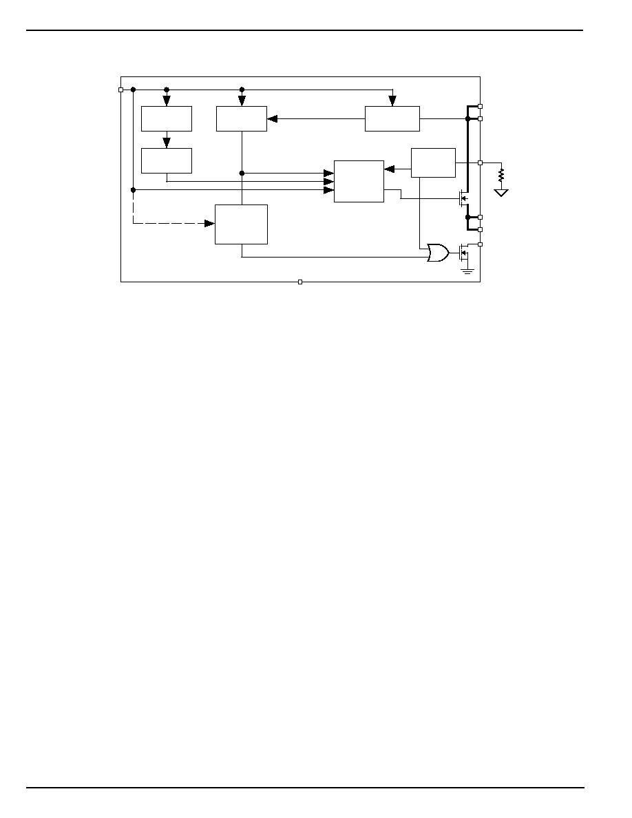
Block Diagram
THERMAL
SHUTDOWN
OSC.
CHARGE
PUMP
OUT
GATE
CONTROL
IN
FLG
EN
CURRENT
LIMIT
GND
ILIM
R
SET
THERMAL
SHUTDOWN
LATCH
(MIC2549A)
RESET
IN
OUT
1.2V
REFERENCE

December 2001
11
MIC2545A/2549A
MIC2545A/2549A
Micrel
Functional Description
The MIC2545A and MIC2549A are high-side N-channel
switches available with active-high or active-low enable in-
puts. Fault conditions turn off or inhibit turn-on of the output
transistor and activate the open-drain error flag transistor
making it sink current to ground.
Input and Output
IN is the power supply connection to the logic circuitry and the
drain of the output MOSFET. OUT is the source of the output
MOSFET. In a typical circuit, current flows from IN to OUT
toward the load. If V
OUT
is greater than V
IN
, current will flow
from OUT to IN since the switch is bidirectional when en-
abled. The output MOSFET and driver circuitry are also
designed to allow the MOSFET source to be externally forced
to a higher voltage than the drain (V
OUT
> V
IN
) when the
switch is disabled. In this situation, the MIC2545A/49A avoids
undesirable current flow from OUT to IN. Both IN pins must
be connected together, and both OUT pins must be con-
nected together.
Thermal Shutdown
Thermal shutdown shuts off the output MOSFET and signals
the fault flag if the die temperature exceeds 135
∞
C. 10
∞
C of
hysteresis prevents the switch from turning on until the die
temperature drops to 125
∞
C. Overtemperature detection
functions only when the switch is enabled.
The MIC2549A features an internal latch which causes the
part to remain off after thermal shutdown until a reset pulse
is provided via the enable pin (pin 1). While in current-limit, the
thermal shutdown latch prevents on/off cycling of the output.
Refer to Figure 2 for timing diagram. The flag remains low
until reset.
Enable Input
EN must be driven logic high or logic low, or be pulled high or
low for a clearly defined input. Floating the input may cause
unpredictable operation. EN should not be allowed to go
negative with respect to GND.
Current-Limit Operation
The current limit is user adjustable with an external set
resistor. Current limiting in the range of 500mA to 3A is
available with a set point accuracy of better than
±
30% (
±
20%
for I
SET
1 to 2.5A). The current-limit circuit prevents damage
to the output MOSFET and external load.
The current-limit response of the MIC2545A/49A is based on
the type of load that is applied to the output and is defined in
three parts:
1. The first mode of operation is where the device
enters a constant-current mode preventing
further increases in output current. The value of
this current, I
LIMIT
, is defined by the value of
R
SET
as explained further in this section.
2. When a short circuit is applied to the output of
an enabled device the output current immedi-
ately folds back to a value less than I
LIMIT
called
I
SHORT
. This further protects the load and
reduces device power dissipation. Refer to the
"Typical Characteristics: Output Current vs.
Output Voltage" graph for details.
3. When a load is increased, the output current will
proportionally increase up to the current-limit
threshold, I
TH
, as shown in the "Functional
Characteristics: Current-Limit Response" graph.
The device in this case will supply current
slightly higher than the current-limit set point
defined by R
SET
. As the load is increased
further the current folds back to I
LIMIT
.
The nominal current-limit value, I
LIMIT
, is set with an external
resistor between ILIM (pin 4) and GND (pin 3). For a desired
current-limit, the value of the external set resistor is given by:
R
=
I
SET
LIMIT
230
where:
76.8
< R
SET
< 459
For example, to set a 1A nominal current-limit, R
SET
is
calculated as:
230
1A
=
230
Refer to the "Typical Characteristics: Current-Limit vs R
SET
"
graph for more details.
Current through R
SET
increases with output current. The
voltage across R
SET
could be monitored with a high imped-
ance comparator to provide an indication of output current.
R
SET
should be between 76.8
and 459
(1% resister
value).
Fault Flag
FLG is an N-channel, open-drain MOSFET output. The fault-
flag is active (low) for current-limit or thermal shutdown
conditions. The flag output MOSFET is capable of sinking a
10mA load to typically 100mV above ground. For applications
with V
IN
3.6V, it is recommended that flag current be limited
to 5mA or less.
MIC2545A/2549A
Micrel
MIC2545A/2549A
12
December 2001
Applications Information
Supply Filtering
A 0.1
µ
F to 1
µ
F bypass capacitor from IN to GND, located near
the MIC2545A and MIC2549A, is strongly recommended to
control supply transients. Without a bypass capacitor, an
output short may cause sufficient ringing on the input (from
supply lead inductance) to damage internal control circuitry.
Input transients must not exceed the absolute maximum
supply voltage (V
IN max
= 6V) even for a short duration.
MIC2549A-1BM
EN
OUT
FLG
GND
OUT
ILIM
IN
IN
1
8
2
7
3
6
4
5
0.1µF to 1µF
4.0V to 5.5V
R
SET
Figure 3. Supply Bypassing
Power Dissipation
The device's junction temperature depends on several fac-
tors such as the load, PCB layout, ambient temperature and
package type. Equations that can be used to calculate power
dissipation and junction temperature are found below.
Calculation of power dissipation can be accomplished by the
following equation:
P
D
= R
DS(on)
◊
(I
OUT
)2
To relate this to junction temperature, the following equation
can be used:
T
J
= P
D
◊
JA
+ T
A
where:
T
J
= junction temperature
T
A
= ambient temperature
JA
= is the thermal resistance of the package
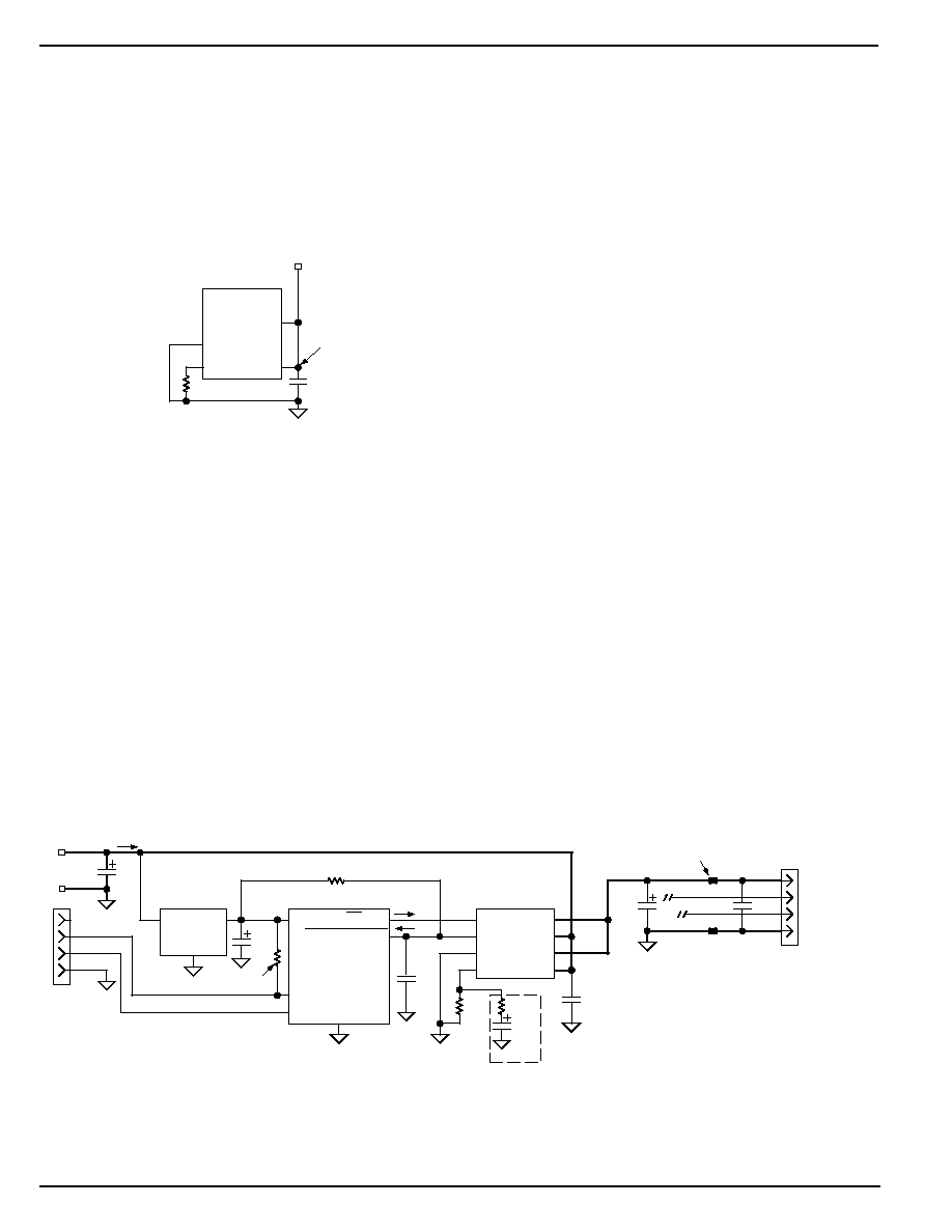
Transient Overcurrent Filter
The inrush current from the connection of a heavy capacitive
load may cause the fault flag to fall for 10
µ
s to 200
µ
s while the
switch is in a constant-current mode, charging the capaci-
tance.
Adding an optional series resistor-capacitor (R
SET2
) in paral-
lel with R
SET
, as shown in Figure 4, allows the transient
current-limit to be set to a different value than steady state. A
typical USB hot-plug inrush is 2A to 3A for 10
µ
s to 20
µ
s. If
R
SET
is 435
(530mA), an R
SET2
of 88
(2.5A) and C
SET
of
1
µ
F (RC
90
µ
s) allows transient surge of 3A to pass for 90
µ
s
without tripping the overcurrent flag (FLG).
USB Power Distribution
The MIC2545A is ideal for meeting USB power distribution
requirements. Figure 7 depicts a USB Host application. R
SET
should be set to a value providing a current-limit >500mA.
The accurate current-limit of the MIC2545A will reduce power
supply current requirements. Also, fast reaction to short
circuit faults prevent voltage droop in mobile PC applications.
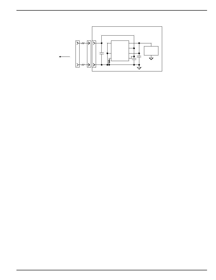
Printed Circuit Board Hot-Plug
The MIC2545A/49A is an ideal inrush current-limiter suitable
for hot-plug applications. Due to the integrated charge pump,
the MIC2545A/49A presents a high impedance when off and
slowly becomes a low impedance as it turns on. This "soft-
start" feature effectively isolates power supplies from highly
capacitive loads by reducing inrush current during hot-plug
events. Figure 5 shows how the MIC2545A may be used in
a hot-plug application.
ON/OFF
OVERCURRENT
MIC2545A-2
3.3V USB Controller
V
BUS
D+
D≠
GND
10k
MIC5203-3.3
LDO Regulator
IN
OUT
GND
Ferrite
Bead
V
BUS
D+
D≠
GND
D+
D≠
V+
EN
OUT
FLG
IN
GND
OUT
ILIM
IN
Bold lines indicate
0.1" wide, 1-oz. copper
high-current traces.
Downstream
USB
Port 1
4.75V min.
500mA max.
120µF
0.01µF
1.0
µF
GND
0.1µF
5V
(+)
(≠)
4.7µF
R
SET
R
SET(2)
(optional)
C
SET
1.5k
2%
0.1µF
Figure 4. USB Host Application
December 2001
13
MIC2545A/2549A
MIC2545A/2549A
Micrel
MIC2545A-2
EN
OUT
FLG
GND
OUT
IN
IN
1
8
2
7
3
6
5
I
LIM
4
Adaptor Card
to "Hot"
Receptacle
C
BULK
GND
V
CC
0.1
µF
Backend
Function
0.1µF
Figure 5. Hot-Plug Application
MIC2545A/2549A
Micrel
MIC2545A/2549A
14
December 2001
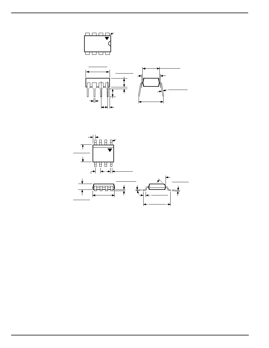
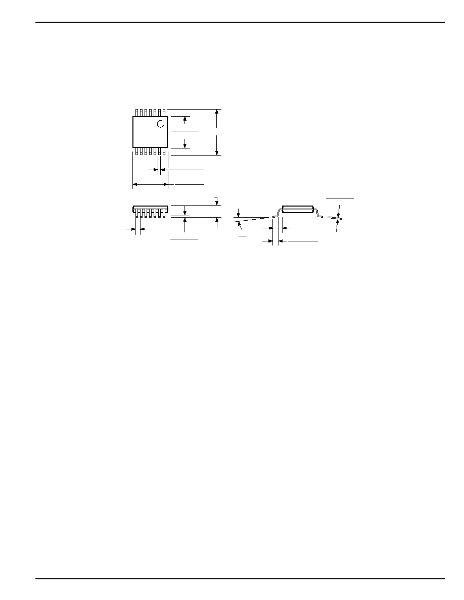
Package Information
0.380 (9.65)
0.370 (9.40)
0.135 (3.43)
0.125 (3.18)
PIN 1
DIMENSIONS:
INCH (MM)
0.018 (0.57)
0.100 (2.54)
0.013 (0.330)
0.010 (0.254)
0.300 (7.62)
0.255 (6.48)
0.245 (6.22)
0.380 (9.65)
0.320 (8.13)
0.0375 (0.952)
0.130 (3.30)
8-Pin DIP (N)
45
∞
0
∞
≠8
∞
0.244 (6.20)
0.228 (5.79)
0.197 (5.0)
0.189 (4.8)
SEATING
PLANE
0.026 (0.65)
MAX
)
0.010 (0.25)
0.007 (0.18)
0.064 (1.63)
0.045 (1.14)
0.0098 (0.249)
0.0040 (0.102)
0.020 (0.51)
0.013 (0.33)
0.157 (3.99)
0.150 (3.81)
0.050 (1.27)
TYP
PIN 1
DIMENSIONS:
INCHES (MM)
0.050 (1.27)
0.016 (0.40)
8-Pin SOIC (M)
December 2001
15
MIC2545A/2549A
MIC2545A/2549A
Micrel
1.10 MAX (0.043)
0.15 (0.006)
0.05 (0.002)
1.00 (0.039) REF
0.65 BSC
(0.026)
8
∞
0
∞
6.4 BSC (0.252)
5.10 (0.200)
4.90 (0.193)
0.20 (0.008)
0.09 (0.003)
0.70 (0.028)
0.50 (0.020)
DIMENSIONS:
MM (INCH)
4.50 (0.177)
4.30 (0.169)
0.30 (0.012)
0.19 (0.007)
14-Pin TSSOP (TS)

MIC2545A/2549A
Micrel
MIC2545A/2549A
16
December 2001
MICREL INC.
1849 FORTUNE DRIVE
SAN JOSE, CA 95131
USA
TEL
+ 1 (408) 944-0800
FAX
+ 1 (408) 944-0970
WEB
http://www.micrel.com
This information is believed to be accurate and reliable, however no responsibility is assumed by Micrel for its use nor for any infringement of patents or
other rights of third parties resulting from its use. No license is granted by implication or otherwise under any patent or patent right of Micrel Inc.
© 2001 Micrel Incorporated